

Page 1
查询CS8190供应商
CS8190
Precision Air-Core
Tach/Speedo Driver with
Return to Zero
The CS8190 is specifically designed for use with air–core meter
movements. The IC provides all the functions necessary for an analog
tachometer or speedometer. The CS8190 takes a speed sensor input
and generates sine and cosine related output signals to differentially
drive an air–core meter.
Many enhancements have been added over industry standard
tachometer drivers such as the CS289 or LM1819. The output utilizes
differential drivers which eliminates the need for a zener reference
and offers more torque. The device withstands 60 V transients which
decreases the protection circuitry required. The device is also more
precise than existing devices allowing for fewer trims and for use in a
speedometer.
Features
• Direct Sensor Input
• High Output Torque
• Low Pointer Flutter
• High Input Impedance
• Overvoltage Protection
• Return to Zero
• Internally Fused Leads in DIP–16 and SO–20L Packages
16
http://onsemi.com
1
DIP–16
NF SUFFIX
CASE 648
PIN CONNECTIONS AND
MARKING DIAGRAM
DIP–16
SQ
FREQ
OUT
IN
CC
CS8190ENF16
AWLYYWW
20
SO–20L
DWF SUFFIX
CASE 751D
161
CP–CP+
F/V
OUT
V
REG
GNDGND
GNDGND
SINE+COS+
SINE–COS–
BIASV
1
SO–20L
1
SQ
OUT
FREQ
IN
GND
GND
CC
A = Assembly Location
WL, L = Wafer Lot
YY, Y = Year
WW, W = Work Week
AWLYYWW
CS–8190
20
CP–CP+
F/V
V
REG
GNDGND
GND
GND
GNDGND
SIN+COS+
SIN–COS–
BIASV
OUT
ORDERING INFORMATION
Device Package Shipping
CS8190ENF16 DIP–16 25 Units/Rail
CS8190EDWF20 SO–20L
CS8190EDWFR20 SO–20L 1000 Tape & Reel
37 Units/Rail
Semiconductor Components Industries, LLC, 2001
March, 2001 – Rev . 4
1 Publication Order Number:
CS8190/D
Page 2
CS8190
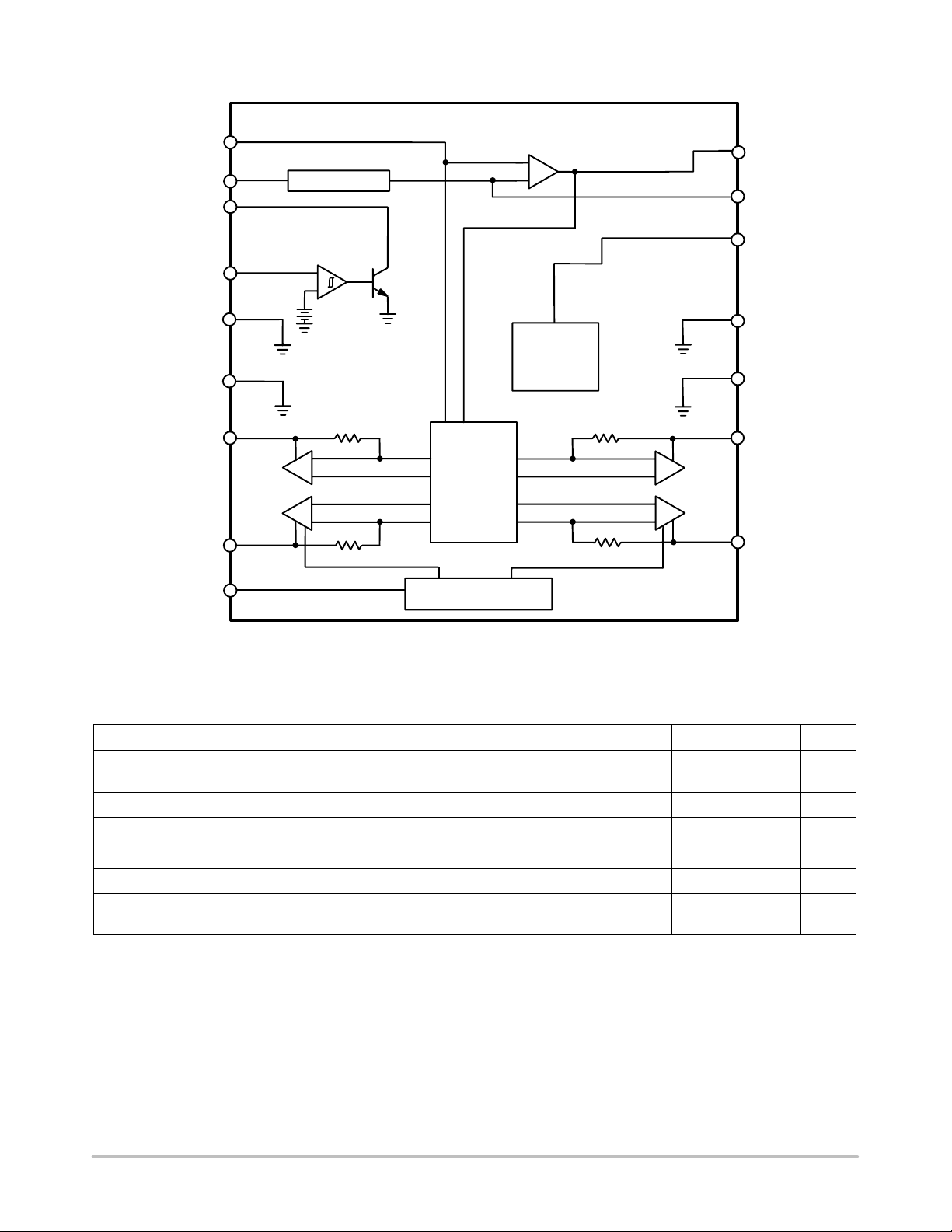
BIAS
CP+
SQ
FREQ
GND
GND
COS+
COS–
V
OUT
CC
F/V
OUT
Charge Pump
+
-
CP–
Input
Comp.
IN
+
-
Voltage
V
REG
Regulator
GND
V
REG
7.0 V
GND
SINE+
COS
Output
+
Func.
Gen.
+
-
+
+
-
SINE
Output
SINE–
High Voltage
Protection
Figure 1. Block Diagram
ABSOLUTE MAXIMUM RATINGS*
Rating Value Unit
Supply Voltage, V
CC
Operating Temperature –40 to +105 °C
Storage Temperature –40 to +165 °C
Junction Temperature –40 to +150 °C
ESD (Human Body Model) 4.0 kV
Lead Temperature Soldering: Wave Solder (through hole styles only) (Note 1.)
1. 10 seconds maximum.
2. 60 second maximum above 183°C.
*The maximum package power dissipation must be observed.
< 100 ms Pulse Transient
Continuous
Reflow: (SMD styles only) (Note 2.)
60
24
260 peak
230 peak
°C
°C
V
V
http://onsemi.com
2
Page 3
CS8190
ELECTRICAL CHARACTERISTICS (–40°C ≤ T
Characteristic
≤ 85°C, 8.5 V ≤ VCC ≤ 15 V, unless otherwise specified.)
A
Test Conditions Min Typ Max Unit
Supply Voltage Section
ICC Supply Current VCC = 16 V, –40°C, No Load – 50 125 mA
VCC Normal Operation Range – 8.5 13.1 16 V
Input Comparator Section
Positive Input Threshold – 1.0 2.0 3.0 V
Input Hysteresis – 200 500 – mV
Input Bias Current (Note 3.) 0 V ≤ VIN ≤ 8.0 V – –10 –80 µA
Input Frequency Range – 0 – 20 kHz
Input Voltage Range in series with 1.0 kΩ –1.0 – V
Output V
SAT
ICC = 10 mA – 0.15 0.40 V
CC
Output Leakage VCC = 7.0 V – – 10 µA
Low VCC Disable Threshold – 7.0 8.0 8.5 V
Logic 0 Input Voltage – 1.0 – – V
Voltage Regulator Section
Output Voltage – 6.25 7.00 7.50 V
Output Load Current – – – 10 mA
Output Load Regulation 0 to 10 mA – 10 50 mV
Output Line Regulation 8.5 V ≤ V
Power Supply Rejection VCC = 13.1 V, 1.0 V
≤ 16 V – 20 150 mV
CC
1.0 kHz 34 46 – dB
P/P
Charge Pump Section
Inverting Input Voltage – 1.5 2.0 2.5 V
Input Bias Current – – 40 150 nA
V
Input Voltage – 1.5 2.0 2.5 V
BIAS
Non Invert. Input Voltage IIN = 1.0 mA – 0.7 1.1 V
Linearity (Note 4.) @ 0, 87.5, 175, 262.5, + 350 Hz –0.10 0.28 +0.70 %
F/V
Gain @ 350 Hz, CCP = 0.0033 µF,
OUT
R
= 243 kΩ
T
7.0 10 13 mV/Hz
Norton Gain, Positive IIN = 15 µA 0.9 1.0 1.1 I/I
Norton Gain, Negative IIN = 15 µA 0.9 1.0 1.1 I/I
Function Generator Section: –40C TA 85°C, VCC = 13.1 V unless otherwise noted.
Return to Zero Threshold TA = 25°C 5.2 6.0 7.0 V
Differential Drive Voltage
(V
COS+
– V
COS–
)
Differential Drive Voltage
(V
– V
SIN–
)
SIN+
Differential Drive Voltage
(V
COS+
– V
COS–
)
Differential Drive Voltage
(V
– V
SIN–
)
SIN+
8.5 V ≤ V
Θ = 0°
8.5 V ≤ V
Θ = 90°
8.5 V ≤ V
Θ = 180°
8.5 V ≤ V
Θ = 270°
CC
CC
CC
CC
≤ 16 V
≤ 16 V
≤ 16 V
≤ 16 V
5.5 6.5 7.5 V
5.5 6.5 7.5 V
–7.5 –6.5 –5.5 V
–7.5 –6.5 –5.5 V
3. Input is clamped by an internal 12 V Zener.
4. Applies to % of full scale (270°).
V
http://onsemi.com
3
Page 4
CS8190
ELECTRICAL CHARACTERISTICS (continued) (–40°C ≤ T
≤ 85°C, 8.5 V ≤ VCC ≤ 15 V, unless otherwise specified.)
A
Characteristic UnitMaxTypMinTest Conditions
Function Generator Section: –40C TA 85°C, VCC = 13.1 V unless otherwise noted. (continued)
Differential Drive Current
8.5 V ≤ V
≤ 16 V – 33 42 mA
CC
Zero Hertz Output Angle – –1.5 0 1.5 deg
Function Generator Error (Note 5.)
Reference Figures 2, 3, 4, 5
VCC = 13.1 V
Θ = 0° to 305°
–2.0 0 +2.0 deg
Function Generator Error 13.1 V ≤ VCC ≤ 16 V –2.5 0 +2.5 deg
Function Generator Error 13.1 V ≤ VCC ≤ 11 V –1.0 0 +1.0 deg
Function Generator Error 13.1 V ≤ VCC ≤ 9.0 V –3.0 0 +3.0 deg
Function Generator Error 25°C ≤ TA ≤ 80°C –3.0 0 +3.0 deg
Function Generator Error 25°C ≤ TA ≤ 105°C –5.5 0 +5.5 deg
Function Generator Error –40°C ≤ TA ≤ 25°C –3.0 0 +3.0 deg
Function Generator Gain TA = 25°C, Θ vs F/V
, 60 77 95 °/V
OUT
5. Deviation from nominal per Table 1 after calibration at 0 ° and 270°.
PIN FUNCTION DESCRIPTION
PACKAGE PIN #
DIP–16
1 1 CP+ Positive input to charge pump.
2 2 SQ
3 3 FREQ
4, 5, 12, 13 4–7, 14–17 GND Ground Connections.
6 8 COS+ Positive cosine output signal.
7 9 COS– Negative cosine output signal.
8 10 V
9 11 BIAS Test point or zero adjustment.
10 12 SIN– Negative sine output signal.
11 13 SIN+ Positive sine output signal.
14 18 V
15 19 F/V
16 20 CP– Negative input to charge pump.
SO–20L
PIN SYMBOL FUNCTION
OUT
IN
CC
REG
OUT
Buffered square wave output signal.
Speed or RPM input signal.
Ignition or battery supply voltage.
Voltage regulator output.
Output voltage proportional to input signal frequency.
http://onsemi.com
4
Page 5
CS8190
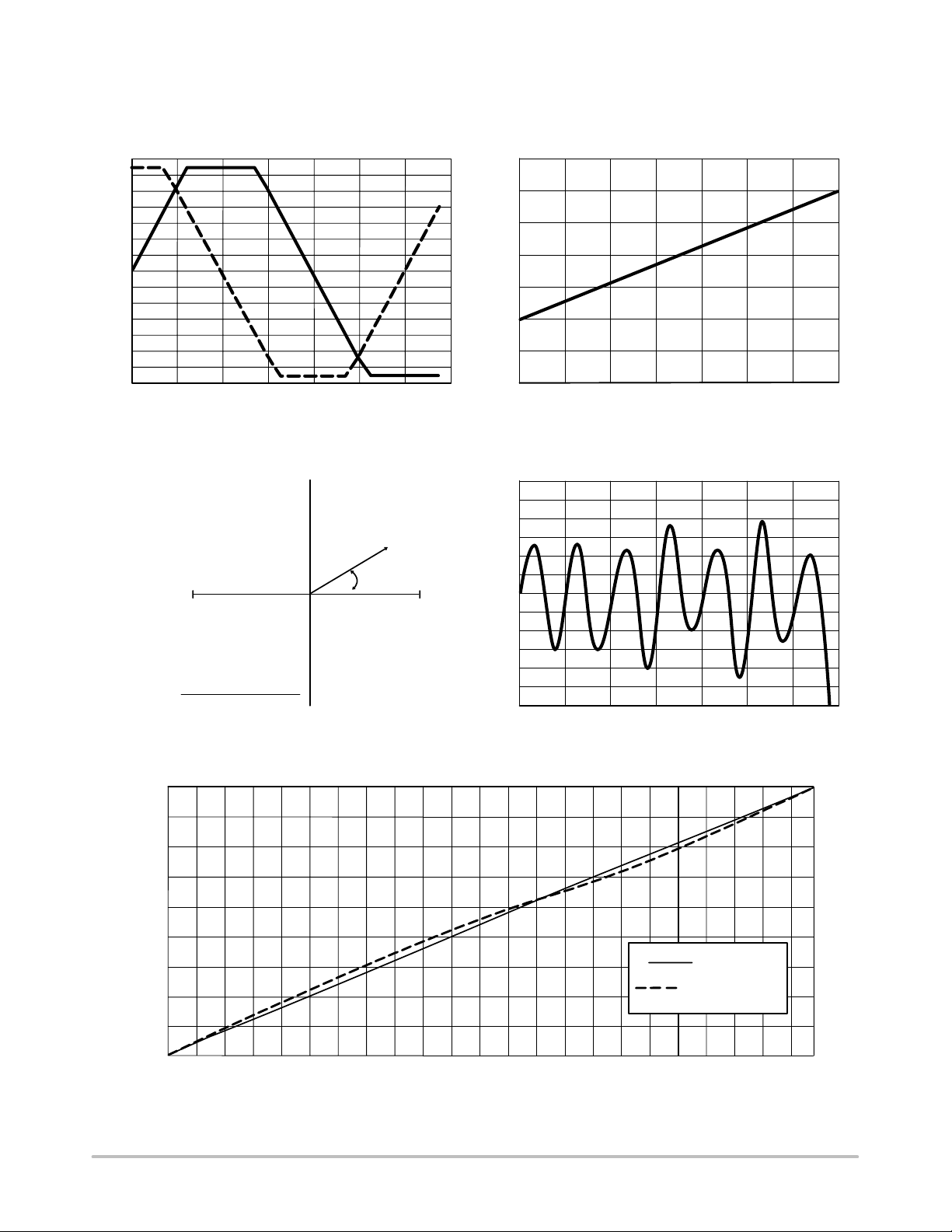
TYPICAL PERFORMANCE CHARACTERISTICS
7
6
5
4
3
2
1
0
–1
–2
Output Voltage (V)
–3
–4
–5
–6
–7
0 45 90 135 180 225 270 315
Degrees of Deflection (°)
Figure 2. Function Generator Output Voltage vs.
Degrees of Deflection
7.0 V
(V
ARCTAN
V
V
COS
SINE+
–7.0 V
SIN
) – (V
V
V
SINE–
SIN
COS
)
Θ
(V
) – (V
COS+
–7.0 V
Figure 4. Output Angle in Polar Form Figure 5. Nominal Output Deviation
Angle
7.0 V
COS–
COS
SIN
FV
2.0 V 2.0 FREQ CCP RT (V
OUT
7
6
5
4
3
F/V Output (V)
2
1
0
0 45 90 135 180 225 270 315
Frequency/Output Angle (°)
REG
0.7 V)
Figure 3. Charge Pump Output Voltage vs.
Output Angle
1.50
1.25
1.00
0.75
0.50
0.25
0.00
–0.25
Deviation (°)
)
–0.50
–0.75
–1.00
–1.25
–1.50
0 45 90 135 180 270 315
Theoretical Angle (°)
225
45
40
35
30
25
20
Ideal Angle (Degrees)
15
10
5
0
1591317 33 41
21
Nominal Angle (Degrees)
25
29
Ideal Degrees
Nominal Degrees
37
Figure 6. Nominal Angle vs. Ideal Angle (After Calibrating at 180)
http://onsemi.com
5
45
Page 6

CS8190
Table 1. Function Generator Output Nominal Angle vs. Ideal Angle (After Calibrating at 270)
Nominal
Ideal
Degrees
0 0 17 17.98 34 33.04 75 74.00 160 159.14 245 244.63
1 1.09 18 18.96 35 34.00 80 79.16 165 164.00 250 249.14
2 2.19 19 19.92 36 35.00 85 84.53 170 169.16 255 254.00
3 3.29 20 20.86 37 36.04 90 90.00 175 174.33 260 259.16
4 4.38 21 21.79 38 37.11 95 95.47 180 180.00 265 264.53
5 5.47 22 22.71 39 38.21 100 100.84 185 185.47 270 270.00
6 6.56 23 23.61 40 39.32 105 106.00 190 190.84 275 275.47
7 7.64 24 24.50 41 40.45 110 110.86 195 196.00 280 280.84
8 8.72 25 25.37 42 41.59 115 115.37 200 200.86 285 286.00
9 9.78 26 26.23 43 42.73 120 119.56 205 205.37 290 290.86
10 10.84 27 27.07 44 43.88 125 124.00 210 209.56 295 295.37
11 11.90 28 27.79 45 45.00 130 129.32 215 214.00 300 299.21
12 12.94 29 28.73 50 50.68 135 135.00 220 219.32 305 303.02
13 13.97 30 29.56 55 56.00 140 140.68 225 225.00
14 14.99 31 30.39 60 60.44 145 146.00 230 230.58
15 16.00 32 31.24 65 64.63 150 150.44 235 236.00
16 17.00 33 32.12 70 69.14 155 154.63 240 240.44
Note: Temperature, voltage and nonlinearity not included.
Degrees
Ideal
Degrees
Nominal
Degrees
Ideal
Degrees
Nominal
Degrees
Ideal
Degrees
Nominal
Degrees
Ideal
Degrees
Nominal
Degrees
Ideal
Degrees
Nominal
Degrees
CIRCUIT DESCRIPTION and APPLICATION NOTES
The CS8190 is specifically designed for use with air–core
meter movements. It includes an input comparator for
sensing an input signal from an ignition pulse or speed
sensor, a charge pump for frequency to voltage conversion,
a bandgap voltage regulator for stable operation, and a
function generator with sine and cosine amplifiers to
differentially drive the meter coils.
From the partial schematic of Figure 7, the input signal is
applied to the FREQ
lead, this is the input to a high
IN
impedance comparator with a typical positive input
threshold of 2.0 V and typical hysteresis of 0.5 V. The output
of the comparator, SQ
, is applied to the charge pump
OUT
input CP+ through an external capacitor CCP. When the
input signal changes state, CCP is charged or discharged
through R3 and R4. The charge accumulated on C
CP
is
mirrored to C4 by the Norton Amplifier circuit comprising
of Q1, Q2 and Q3. The charge pump output voltage, F /V
OUT
ranges from 2.0 V to 6.3 V depending on the input signal
frequency and the gain of the charge pump according to the
formula:
FV
2.0 V 2.0 FREQ CCP RT (V
OUT
REG
0.7 V)
RT is a potentiometer used to adjust the gain of the F/V
output stage and give the correct meter deflection. The F/V
output voltage is applied to the function generator which
generates the sine and cosine output voltages. The output
voltage of the sine and cosine amplifiers are derived from the
on–chip amplifier and function generator circuitry. The
various trip points for the circuit (i.e., 0°, 90°, 180°, 270°)
are determined by an internal resistor divider and the
bandgap voltage reference. The coils are differentially
driven, allowing bidirectional current flow in the outputs,
thus providing up to 305° range of meter deflection. Driving
the coils differentially offers faster response time, higher
current capability, higher output voltage swings, and
reduced external component count. The key advantage is a
higher torque output for the pointer.
The output angle, Θ, is equal to the F/V gain multiplied by
the function generator gain:
A
FV
AFG,
where:
,
AFG 77°V(typ)
The relationship between input frequency and output
angle is:
AFG 2.0 FREQ CCP RT (V
or,
970 FREQ CCP R
The ripple voltage at the F/V converter’s output is
determined by the ratio of CCP and C4 in the formula:
V
CCP(V
REG
C4
0.7 V)
REG
0.7 V)
T
http://onsemi.com
6
Page 7
V
CS8190
REG
FREQ
FREQ
SQ
OUT
2.0 V
R3
0.25 V
V
(t)
C
+
–
CP
R4
Q
SQUARE
C
SQ
IN
OUT
+
–
2.0 V
CP+
Q1 Q2
Q3
CP–
+
–
R
C4
F/V
OUT
F to V
T
Figure 7. Partial Schematic of Input and Charge Pump
T
t
DCHG
V
CC
0
IN
V
REG
t
CHG
0
I
CP+
V
CP+
0
Figure 8. Timing Diagram of FREQIN and I
Ripple voltage on the F/V output causes pointer or needle
flutter especially at low input frequencies.
The response time of the F/V is determined by the time
constant formed by RT and C4. Increasing the value of C4
will reduce the ripple on the F/V output but will also increase
the response time. An increase in response time causes a
very slow meter movement and may be unacceptable for
many applications.
The CS8190 h as a n u ndervoltage d etect c ircuit t hat d isables
the input comparator when V
falls below 8.0 V(typical).
CC
With n o i nput s ignal t he F /V o utput v oltage d ecreases a nd t he
needle moves towards zero. A second undervoltage detect
circuit at 6.0 V(typical) causes the function generator to
CP
generate a dif ferential S IN d rive v oltage o f z ero v olts a nd t he
differential COS drive voltage t o g o a s h igh a s p ossible. T his
combination of voltages (Figure 2) across the meter coil
moves the needle to the 0° position. Connecting a large
capacitor(> 2000 µF) to the V
lead (C2 in Figure 9)
CC
increases the time between these undervoltage points since
the capacitor discharges slowly and ensures that the needle
moves towards 0° as o pposed to 360°. The exact value of the
capacitor depends on the response time of the system,the
maximum meter deflection and the current consumption of
the circuit. It should be s elected b y b readboarding t he d esign
in the lab.
http://onsemi.com
7
Page 8
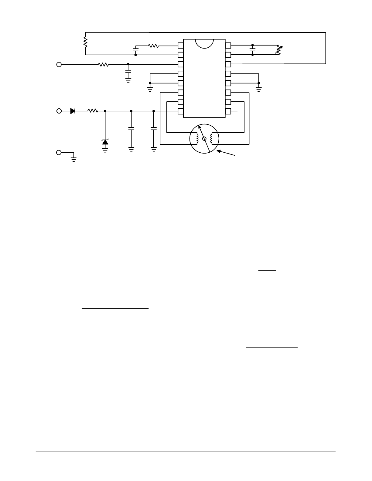
CS8190
Speedo Input
Battery
D1
1.0 A
600 PIV
GND
Notes:
1. C2 (> 2000 µF) is needed if return to zero function is required.
2. The product of C4 and R
3. C4 Range; 20 pF to 0.2 µF.
4. R4 Range; 100 kΩ to 500 kΩ.
5. The IC must be protected from transients above 60 V and reverse battery conditions.
6. Additional filtering on the FREQ
7. Gauge coil connections to the IC must be kept as short as possible (≤ 3.0 inch) for best pointer stability.
R3
3.0 kΩ
10 kΩ
R1
3.9,
500 mW
0.0033 µF
± 30 PPM/°C
R2
C3
0.1 µF
D2
50 V,
500 mW
Zener
C
C1
CP
T
R4
1.0 kΩ
0.1 µF
C2
2000 µF
have a direct effect on gain and therefore directly affect temperature compensation.
IN
COSINE SINE
lead may be required.
1
CP+
SQ
OUT
FREQ
GND
GND
COS+
COS–
V
CC
F/V
IN
CS8190
Air Core
Gauge
200 Ω
CP–
OUT
V
REG
GND
GND
SINE+
SINE–
BIAS
C4
0.47 µF
+
Speedometer
Trim Resistor
R
T
± 20 PPM/°C
Figure 9. Speedometer or Tachometer Application
Design Example
Maximum meter Deflection = 270°
Maximum Input Frequency = 350 Hz
1. Select R
970 FREQ CCP RT 270°
Let CCP = 0.0033 µF, find R
and C
T
R
T
CP
T
270°
970 350 Hz 0.0033 F
RT 243 k
RT should be a 250 kΩ potentiometer to trim out any
inaccuracies due to IC tolerances or meter movement
pointer placement.
2. Select R3 and R4
Resistor R3 sets the output current from the voltage
regulator. The maximum output current from the voltage
regulator is 10 mA. R3 must ensure that the current does not
exceed this limit.
Choose R3 = 3.3 kΩ
The charge current for C
V
REG
3.3 k
CP
0.7 V
is
1.90 mA
CCP must charge and discharge fully during each cycle of
the input signal. Time for one cycle at maximum frequency
is 2.85 ms. To ensure that C
is charged, assume that the
CP
(R3 + R4) C
time constant is less than 10% of the
CP
minimum input period.
T 10%
1
350 Hz
285 s
Choose R4 = 1.0 kΩ.
Discharge time: t
= R3 × CCP = 3.3 kΩ × 0.0033 µF
DCHG
= 10.9 µs
Charge time: t
= (R3 + R4)CCP = 4.3 kΩ. × 0 .0033 µF
CHG
= 14.2 µs
3. Determine C4
C4 is selected to satisfy both the maximum allowable
ripple voltage and response time of the meter movement.
C4
C
CP(VREG
V
0.7 V)
MAX
With C4 = 0.47 µF, the F/V ripple voltage is 44 mV.
The last component to be selected is the return to zero
capacitor C2. This is selected by increasing the input signal
frequency to its maximum so the pointer is at its maximum
deflection, then removing the power from the circuit. C2
should be large enough to ensure that the pointer always
returns to the 0° position rather than 360 ° under all operating
conditions.
Figure 10 shows how the CS8190 and the CS8441 are
used to produce a Speedometer and Odometer circuit.
http://onsemi.com
8
Page 9

R4
CS8190
Input
Battery
600 PIV
GND
D1
1.0 A
R3
R2
10 kΩ
500 mW
R1
3.9,
3.0 kΩ
C3
0.0033 µF
± 30 PPM/°C
0.1 µF
D2
50 V,
500 mW
Zener
C1
0.1 µF
CP
1.0 kΩ
1
CP+
SQ
OUT
FREQ
GND
GND
COS+
COS–
V
CC
IN
CP–
F/V
OUT
V
REG
GND
GND
CS8190
SINE+
SINE–
BIAS
C4
+Speedo
0.47 µF
Trim Resistor
R
T
± 20 PPM/°C
243 kΩ
C
COSINE SINE
Speedometer
C2
10 µF
Air Core
Gauge
200 Ω
1
CS8441
Notes:
Air Core
Stepper
Motor
200 Ω
Odometer
1. C2 = 10 µF with CS8441 application.
2. The product of C4 and R
have a direct effect on gain and therefore directly affect temperature compensation.
T
3. C4 Range; 20 pF to 0.2 µF.
4. R4 Range; 100 kΩ to 500 kΩ.
5. The IC must be protected from transients above 60 V and reverse battery conditions.
6. Additional filtering on the FREQ
lead may be required.
IN
7. Gauge coil connections to the IC must be kept as short as possible (≤ 3.0 inch) for best pointer stability.
Figure 10. Speedometer With Odometer or Tachometer Application
http://onsemi.com
9
Page 10
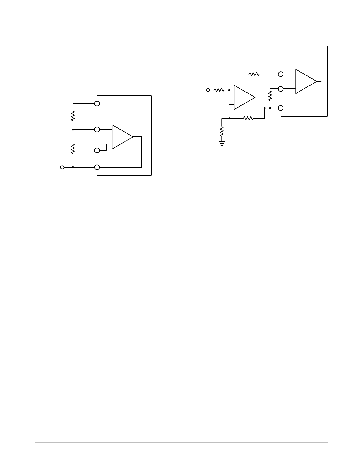
CS8190
In some cases a designer may wish to use the CS8190 only
as a driver for an air–core meter having performed the F/V
conversion elsewhere in the circuit.
Figure 11 shows how to drive the CS8190 with a DC
voltage ranging from 2.0 V t o 6 .0 V. This is a ccomplished b y
forcing a voltage o n the F /V
lead. T he a lternative scheme
OUT
shown in Figure 12 uses an external op amp as a buffer and
operates over an input voltage range of 0 V to 4.0 V.
V
REG
100 kΩ
10 kΩ
V
IN
2.0 V to 6.0 V DC
N/C
Figure 11. Driving the CS8190 from an External
DC Voltage
CP–
F/V
CS8190
–
+
BIAS
OUT
Figures 11 and 12 are not temperature compensated.
CS8190
100 kΩ
100 kΩ
V
IN
0 V to 4.0 V DC
100 kΩ
+
–
100 kΩ
10 kΩ
Figure 12. Driving the CS8190 from an External
DC Voltage Using an Op Amp Buffer
BIAS
CP–
F/V
+
–
OUT
http://onsemi.com
10
Page 11
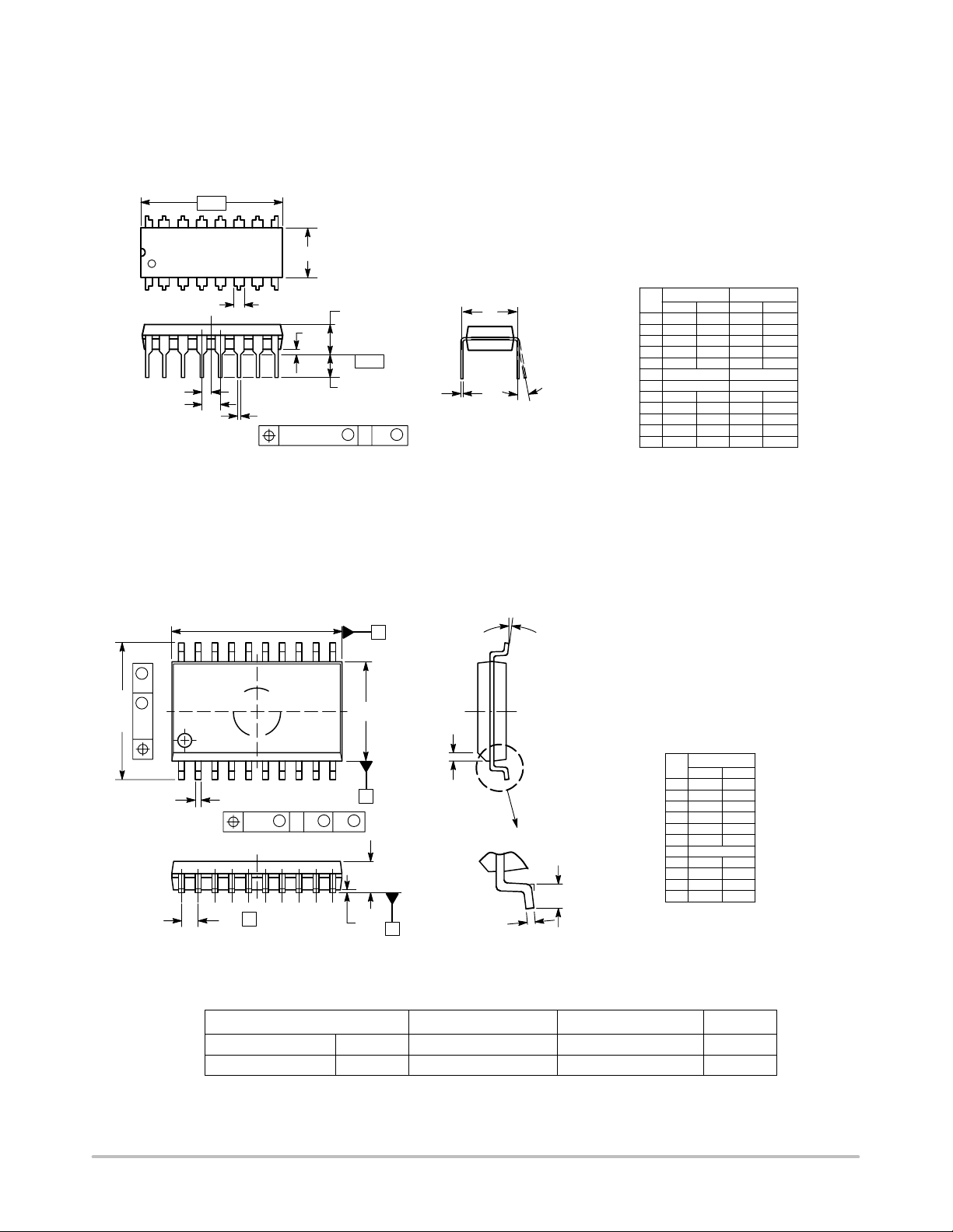
PACKAGE DIMENSIONS
–A–
916
B
18
F
H
G
D
16 PL
0.25 (0.010) T
C
S
–T–
K
M
A
SEATING
PLANE
M
CS8190
DIP–16
NF SUFFIX
CASE 648–08
ISSUE R
L
J
NOTES:
1. DIMENSIONING AND TOLERANCING PER ANSI
Y14.5M, 1982.
2. CONTROLLING DIMENSION: INCH.
3. DIMENSION L TO CENTER OF LEADS WHEN
FORMED PARALLEL.
4. DIMENSION B DOES NOT INCLUDE MOLD FLASH.
5. ROUNDED CORNERS OPTIONAL.
DIM MIN MAX MIN MAX
A 0.740 0.770 18.80 19.55
B 0.250 0.270 6.35 6.85
C 0.145 0.175 3.69 4.44
D 0.015 0.021 0.39 0.53
F 0.040 0.70 1.02 1.77
G 0.100 BSC 2.54 BSC
M
H 0.050 BSC 1.27 BSC
J 0.008 0.015 0.21 0.38
K 0.110 0.130 2.80 3.30
L 0.295 0.305 7.50 7.74
M 0 10 0 10
S 0.020 0.040 0.51 1.01
MILLIMETERSINCHES
H10X
M
B
M
0.25
SO–20L
DWF SUFFIX
CASE 751D–05
ISSUE F
D
20
A
11
E
1
B20X
M
0.25
T
10
SAS
B
B
h X 45
A
L
18X
SEATING
e
A1
T
PLANE
C
NOTES:
1. DIMENSIONS ARE IN MILLIMETERS.
2. INTERPRET DIMENSIONS AND TOLERANCES
PER ASME Y14.5M, 1994.
3. DIMENSIONS D AND E DO NOT INCLUDE MOLD
PROTRUSION.
4. MAXIMUM MOLD PROTRUSION 0.15 PER SIDE.
5. DIMENSION B DOES NOT INCLUDE DAMBAR
PROTRUSION. ALLOWABLE PROTRUSION SHALL
BE 0.13 TOTAL IN EXCESS OF B DIMENSION AT
MAXIMUM MATERIAL CONDITION.
MILLIMETERS
DIM MIN MAX
A 2.35 2.65
A1 0.10 0.25
B 0.35 0.49
C 0.23 0.32
D 12.65 12.95
E 7.40 7.60
e 1.27 BSC
H 10.05 10.55
h 0.25 0.75
L 0.50 0.90
0 7
PACKAGE THERMAL DATA
Parameter
R
Θ
JC
R
Θ
JA
Typical 15 9 °C/W
Typical 50 55 °C/W
DIP–16 SO–20L Unit
http://onsemi.com
11
Page 12

CS8190
ON Semiconductor and are trademarks of Semiconductor Components Industries, LLC (SCILLC). SCILLC reserves the right to make changes
without further notice to any products herein. SCILLC makes no warranty, representation or guarantee regarding the suitability of its products for any particular
purpose, nor does SCILLC assume any liability arising out of the application or use of any product or circuit, and specifically disclaims any and all liability,
including without limitation special, consequential or incidental damages. “Typical” parameters which may be provided in SCILLC data sheets and/or
specifications can and do vary in different applications and actual performance may vary over time. All operating parameters, including “Typicals” must be
validated for each customer application by customer’s technical experts. SCILLC does not convey any license under its patent rights nor the rights of others.
SCILLC products are not designed, intended, or authorized for use as components in systems intended for surgical implant into the body, or other applications
intended to support or sustain life, or for any other application in which the failure of the SCILLC product could create a situation where personal injury or
death may occur. Should Buyer purchase or use SCILLC products for any such unintended or unauthorized application, Buyer shall indemnify and hold
SCILLC and its officers, employees, subsidiaries, affiliates, and distributors harmless against all claims, costs, damages, and expenses, and reasonable
attorney fees arising out of, directly or indirectly, any claim of personal injury or death associated with such unintended or unauthorized use, even if such claim
alleges that SCILLC was negligent regarding the design or manufacture of the part. SCILLC is an Equal Opportunity/Affirmative Action Employer.
PUBLICATION ORDERING INFORMATION
NORTH AMERICA Literature Fulfillment:
Literature Distribution Center for ON Semiconductor
P.O. Box 5163, Denver, Colorado 80217 USA
Phone: 303–675–2175 or 800–344–3860 Toll Free USA/Canada
Fax: 303–675–2176 or 800–344–3867 Toll Free USA/Canada
Email: ONlit@hibbertco.com
Fax Response Line: 303–675–2167 or 800–344–3810 Toll Free USA/Canada
N. American Technical Support: 800–282–9855 Toll Free USA/Canada
EUROPE: LDC for ON Semiconductor – European Support
German Phone: (+1) 303–308–7140 (Mon–Fri 2:30pm to 7:00pm CET)
Email: ONlit–german@hibbertco.com
French Phone: (+1) 303–308–7141 (Mon–Fri 2:00pm to 7:00pm CET)
Email: ONlit–french@hibbertco.com
English Phone: (+1) 303–308–7142 (Mon–Fri 12:00pm to 5:00pm GMT)
Email: ONlit@hibbertco.com
EUROPEAN TOLL–FREE ACCESS*: 00–800–4422–3781
*Available from Germany, France, Italy, UK, Ireland
CENTRAL/SOUTH AMERICA:
Spanish Phone: 303–308–7143 (Mon–Fri 8:00am to 5:00pm MST)
Email: ONlit–spanish@hibbertco.com
ASIA/PACIFIC: LDC for ON Semiconductor – Asia Support
Phone: 303–675–2121 (Tue–Fri 9:00am to 1:00pm, Hong Kong Time)
Toll Free from Hong Kong & Singapore:
001–800–4422–3781
Email: ONlit–asia@hibbertco.com
JAPAN: ON Semiconductor, Japan Customer Focus Center
4–32–1 Nishi–Gotanda, Shinagawa–ku, Tokyo, Japan 141–0031
Phone: 81–3–5740–2745
Email: r14525@onsemi.com
ON Semiconductor Website: http://onsemi.com
For additional information, please contact your local
Sales Representative.
http://onsemi.com
12
CS8190/D
 Loading...