

查询CS8183YDWF20供应商
CS8183
Dual Micropower 200 mA
Low Dropout Tracking
Regulator/Line Driver
The CS8183 is a dual low dropout tracking regulator designed to
provide adjustable buffered output voltages that closely track
(±10 mV) the reference inputs. The outputs deliver up to 200 mA
while being able to be configured higher, lower or equal to the
reference voltages.
The outputs have been designed to operate over a wide range (2.8 V
to 45 V) while still maintaining excellent DC characteristics. The
CS8183 is protected from reverse battery, short circuit and thermal
runaway conditions. The device also can withstand 45 V load dump
transients and −50 V reverse polarity input voltage transients. This
makes it suitable for use in automotive environments.
The V
provide the input voltage as a reference for the output and they also
can be pulled low to place the device in sleep mode where it nominally
draws less than 30 µA from the supply.
The two trackers can be combined in parallel doubling the capability
to 400 mA for a single application.
Features
• Two Regulated Outputs 200 mA, ±10 mV Track Worst Case
• Low Dropout (0.35 V typ. @ 200 mA)
• Low Quiescent Current
• Independent Thermal Shutdown
• Short Circuit Protection
• Wide Operating Range
• Internally Fused Leads in the SO−20L Package
/ENABLE leads serve two purposes. They are used to
REF
http://onsemi.com
20
SO−20L
DWF
SUFFIX
CASE 751D
PIN CONNECTIONS AND
MARKING DIAGRAM
1
V
IN1
V
OUT1
GND
GND
V
REF
ADJ1
/ENABLE1
A = Assembly Location
WL, L = Wafer Lot
YY, Y = Year
WW, W = Work Week
AWLYYWW
1
CS8183
20
V
OUT2
V
IN2
NCNC
NCNC
GND
GND
NCNC
NCNC
V
REF
V
ADJ2
/ENABLE2V
Semiconductor Components Industries, LLC, 2004
March, 2004 − Rev. 15
ORDERING INFORMATION
Device Package Shipping
CS8183YDWF20
CS8183YDWFR20
1 Publication Order Number:
SO−20L
SO−20L
37 Units/Rail
1000 Tape & Reel
CS8183/D
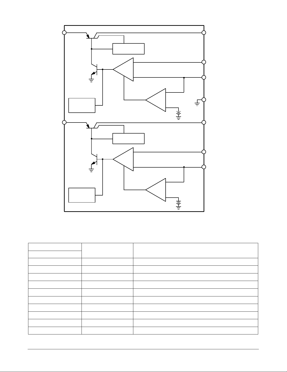
CS8183
V
IN1
V
OUT1
Current Limit &
VSAT Sense
−
ENABLE
+
Adj1
V
REF
/ENABLE1
+
Independent
Thermal
Shutdown
V
IN2
−
2.0 V
GND
V
OUT2
Current Limit &
VSAT Sense
−
ENABLE
+
Adj2
V
REF
/ENABLE2
Independent
Thermal
Shutdown
Figure 1. Block Diagram
PACKAGE PIN DESCRIPTION
Package Lead Number
SO−20L
1 V
2 V
3, 4, 7, 8, 13, 14, 17, 18 NC No connection.
5, 6, 15, 16 GND Ground (4 leads fused)
9 V
10 V
11 V
12 V
19 V
20 V
Lead Symbol Function
IN1
OUT1
ADJ1
/ENABLE1 Reference voltage and ENABLE input for V
REF
ADJ2
/ENABLE2 Reference voltage and ENABLE input for V
REF
IN2
OUT2
Input voltage for V
Regulated output voltage 1.
Adjust lead for V
Adjust lead for V
Input voltage for V
Regulated output voltage 2.
+
−
OUT1
OUT1
OUT2
OUT2
2.0 V
.
.
.
OUT1
.
.
OUT2
.
http://onsemi.com
2
CS8183
MAXIMUM RATINGS*
Rating Value Unit
Storage Temperature −65 to 150 °C
Supply Voltage Range (continuous) 15 to 45 V
Supply Voltage Range (normal, continuous) 3.4 to 45 V
Peak Transient Voltage (VIN = 14 V, Load Dump Transient = 31 V) 45 V
Voltage Range (Adj, V
Maximum Junction Temperature 150 °C
Package Thermal Resistance:
Junction−to−Case, R
Junction−to−Ambient, R
ESD Capability (Human Body Model)
(Machine Model)
Lead Temperature Soldering: Reflow: (SMD styles only) (Note 1) 240 peak
1. 60 second maximum above 183°C.
2. −5°C/+0°C allowable conditions.
*The maximum package power dissipation must be observed.
/ENABLE, V
REF
θ
JC
θ
JA
) −10 to 45 V
OUT
18
73
2.0
200
(Note 2)
°C/W
°C/W
kV
V
°C
ELECTRICAL CHARACTERISTICS (V
0.1 Ω < C
OUT − ESR
< 1.0 Ω @ 10 kHz; unless otherwise stated.)
Parameter
= 14 V; V
IN
/ENABLE > 2.75 V; −40°C ≤ TJ ≤ +125°C; C
REF
OUT
≥ 10 µF;
Test Conditions Min Typ Max Unit
Regular Output 1, 2
V
− V
REF
OUT
V
Tracking Error
OUT
Dropout Voltage (VIN − V
OUT
) I
4.5 V ≤ VIN ≤ 26 V, 100 µA ≤ I
= 100 µA
OUT
I
= 200 mA
OUT
≤ 200 mA, Note 3 −10 − 10 mV
OUT
−
−
100
350
150
600
Line Regulation 4.5 V ≤ VIN ≤ 26 V, Note 3 − − 10 mV
Load Regulation 100 µA ≤ I
≤ 200 mA, Note 3 − − 10 mV
OUT
Adj Lead Current Loop in Regulation − 0.2 1.0 µA
Current Limit VIN = 14 V, V
Quiescent Current (IIN − I
Reverse Current V
) VIN = 12 V, I
OUT
V
IN
V
IN
OUT
= 12 V, I
= 12 V, V
= 5.0 V, VIN = 0 V − 0.2 1.5 mA
= 5.0 V, V
REF
= 200 mA
OUT
= 100 µA
OUT
/ENABLE = 0 V
REF
= 90% of V
OUT
, Note 3 225 − 700 mA
REF
−
−
−
15
75
30
25
150
55
Ripple Rejection f = 120 Hz, IOUT = 200 mA, 4.5 V ≤ VIN ≤ 26 V 60 − − dB
Thermal Shutdown − 150 180 210 °C
V
/ENABLE 1, 2
REF
Enable Voltage
Input Bias Current V
3. V
connected to Adj lead.
OUT
/ENABLE 1, 2 > 2.0 V − 0.2 1.0 µA
REF
− 0.80 2.00 2.75 V
mV
mV
mA
µA
µA
http://onsemi.com
3
 Loading...