

查询CS8129YDW16G供应商
CS8129
5.0 V, 750 mA Low Dropout
Linear Regulator with
Lower RESET Threshold
The CS8129 is a precision 5.0 V linear regulator capable of sourcing
750 mA. The RESET threshold voltage has been lowered to 4.2 V so
that the regulator can be used with 4.0 V microprocessors. The lower
RESET threshold also permits operation under low battery conditions
(5.5 V plus a diode). The RESET’s delay time is externally
programmed using a discrete RC network. During powerup, or when
the output goes out of regulation, RESET remains in the low state for
the duration of the delay. This function is independent of the input
voltage and will function correctly as long as the output voltage
remains at or above 1.0 V. Hysteresis is included in the Delay and the
RESET comparators to improve noise immunity. A latching discharge
circuit is used to discharge the delay capacitor when it is triggered by a
brief fault condition.
The regulator is protected against a variety of fault conditions: i.e.
reverse battery, overvoltage, short circuit and thermal runaway
conditions. The regulator is p rotected a gainst v olt age t ransient s r a nging
from −5 0 V to +40 V. Short c ircuit current is limite d to 1.2 A ( typ).
The CS8129 is packaged in a 5 lead TO−220 and a 16 lead surface
mount package.
Features
• 5.0 V ±3.0% Regulated Output
• Low Dropout Voltage (0.6 V @ 0.5 A)
• 750 mA Output Current Capability
• Reduced RESET Threshold for Use with 4.0 V Microprocessors
• Externally Programmed RESET Delay
• Fault Protection
− Reverse Battery
− 60 V, −50 V Peak Transient Voltage
− Short Circuit
− Thermal Shutdown
• Pb−Free Packages are Available*
http://onsemi.com
TO−220
FIVE LEAD
T SUFFIX
CASE 314D
1
5
TO−220
FIVE LEAD
1
1
5
16
1
See detailed ordering and shipping information in the package
dimensions section on page 8 of this data sheet.
See general marking information in the device marking
section on page 8 of this data sheet.
ORDERING INFORMATION
DEVICE MARKING INFORMATION
TVA SUFFIX
CASE 314K
TO−220
FIVE LEAD
THA SUFFIX
CASE 314A
SO−16WB
DW SUFFIX
CASE 751G
*For additional information on our Pb−Free strategy and soldering details, please
download the ON Semiconductor Soldering and Mounting Techniques
Reference Manual, SOLDERRM/D.
© Semiconductor Components Industries, LLC, 2006
June, 2006 − Rev. 8
1 Publication Order Number:
CS8129/D
CS8129
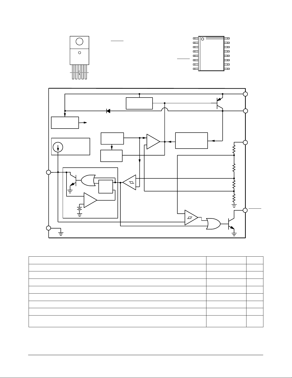
PIN CONNECTIONS
TO−220 5−LEAD
1
Pre−Regulator
Charge
Current
Generator
Pin 1. V
IN
2. RESET
3. GND
4. Delay
5. V
OUT
Regulated Supply
for Circuit Bias
Bandgap
Reference
Thermal
Shutdown
Over Voltage
Shutdown
Error
Amplifier
−
+
1
V
IN
NC
NC
GND
GND
RESET
Delay
Anti−Saturation
and
Current Limit
SO−16 WB
16
V
OUT
NC
V
OUT(SENSE)
GND
GND
GND
NCNC
NC
V
IN
V
OUT
V
OUT
(SENSE)
Delay
Latching Discharge
−
S
Q
+
R
−
+
V
DISCHARGE
+
Delay
Comparator
RESET
−
GND
Figure 1. Block Diagram
ABSOLUTE MAXIMUM RATINGS
Rating Value Unit
Input Operating Range −0.5 to 26 V
Power Dissipation Internally Limited −
Peak Transient Voltage (46 V Load Dump @ 14 V VIN) −50, 60 V
Output Current Internally Limited −
Electrostatic Discharge (Human Body Model) 4.0 kV
Junction Temperature −55 to +150 °C
Storage Temperature Range −55 to +150 °C
Lead Temperature Soldering: Wave Solder (through hole styles only) (Note 1)
Reflow (SMD styles only) (Note 2)
Stresses exceeding Maximum Ratings may damage the device. Maximum Ratings are stress ratings only. Functional operation above the
Recommended Operating Conditions is not implied. Extended exposure to stresses above the Recommended Operating Conditions may affect
device reliability.
1. 10 second maximum.
2. 60 seconds max above 183°C.
260 peak
230 peak
°C
http://onsemi.com
2
CS8129
ELECTRICAL CHARACTERISTICS (−40°C ≤ T
R
RESET
= 4.7 kW to V
unless otherwise noted.) (Note 3)
OUT
≤ 125°C, −40 ≤ TJ ≤ 150°C, 6.0 ≤ VIN ≤ 26 V, 5.0 mA ≤ I
A
≤ 500 mA,
OUT
Characteristic Test Conditions Min Typ Max Unit
OUTPUT STAGE (V
OUT)
Output Voltage − 4.85 5.0 5.15 V
Dropout Voltage I
Supply Current I
Line Regulation 6.0 V ≤ VIN ≤ 26 V, I
Load Regulation 50 mA ≤ I
Ripple Rejection f = 120 Hz, VIN = 7.0 to 17 V, I
= 500 mA − 0.35 0.60 V
OUT
OUT
I
OUT
I
OUT
= 10 mA
= 100 mA
= 500 mA
OUT
= 50 mA − 5.0 50 mV
OUT
≤ 500 mA, VIN = 14 V − 10 50 mV
= 250 mA 54 75 − dB
OUT
−
−
−
2.0
6.0
55
7.0
12
100
Current Limit − 0.75 1.20 − A
Overvoltage Shutdown − 32 − 40 V
Reverse Polarity Input Voltage DC
V
≥ −0.6 V, 10 W Load
OUT
−15 −30 − V
Thermal Shutdown Guaranteed by Design 150 180 210 °C
RESET AND DELAY FUNCTIONS
Delay Charge Current V
RESET Threshold V
RESET Hysteresis VRH = V
Delay Threshold Charge, V
Delay Hysteresis
RESET Output Voltage Low
RESET Output Leakage V
Delay Capacitor Discharge Voltage Discharge Latched “ON”, V
Delay Time
= 2.0 V 5.0 10 15
DELAY
Increasing, V
OUT
V
Decreasing, V
OUT
RT(ON)
Discharge, V
1.0 V < V
OUT
C
DELAY
DC(HI)
OUT
> V
RT(H)
= 0.1 mF, (Note 4)
RT(ON)
RT(OFF)
− V
RT(OFF)
DC(LO)
−
< V
, 3.0 kW to V
RT(L)
Current − 0 10
OUT
> V
OUT
RT
4.05
4.00
50 150 250 mV
3.25
2.85
200 400 800 mV
− 0.1 0.4 V
− 0.2 0.5 V
16 32 48 ms
4.35
4.20
3.50
3.10
4.50
4.45
3.75
3.35
3. To observe safe operating junction temperatures, low duty cycle pulse testing is used in tests where applicable.
4. Assuming ideal capacitor.
C
V
Delay Time +
Delay
Delay Threshold Charge
I
Charge
+ C
3.5 105(typ)
Delay
mA
mA
mA
mA
V
V
V
V
mA
PACKAGE LEAD DESCRIPTION
PACKAGE LEAD #
TO−220
SO−16WB
1 1 V
16 5 V
5 LEAD
LEAD SYMBOL FUNCTION
IN
OUT
Unregulated supply voltage to IC.
Regulated 5.0 V output.
4, 5, 11, 12, 13 3 GND Ground Connection.
8 4 Delay Timing capacitor for RESET function.
6 2 RESET CMOS/TTL compatible output lead. RESET goes low whenever V
below 6.0% of it’s regulated value.
14 N/A V
OUT(SENSE)
Remote sensing of output voltage.
http://onsemi.com
3
OUT
drops
CS8129
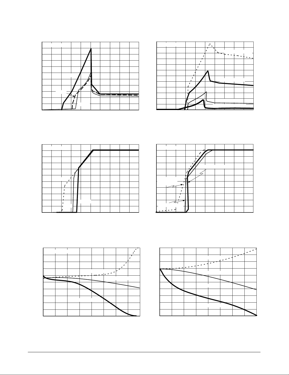
120
55
TYPICAL PERFORMANCE CHARACTERISTICS
R
= 25 W
LOAD
50
45
40
35
30
(mA)
25
CQ
I
125°C
20
15
25°C
10
5
0
01234 6 8 105
Figure 2. Quiescent Current vs. Input Voltage
5.5
R
= 25 W
5.0
LOAD
4.5
4.0
3.5
3.0
(V)
OUT
V
2.5
2.0
125°C
1.5
1.0
0.5
0
01234 6 8 105
25°C
Figure 4. Output Voltage vs. Input Voltage
−40°C
VIN (V)
Over Temperature
−40°C
VIN (V)
Over Temperature
Room Temp
R
= 6.67 W
100
LOAD
80
. (mA)
CQ
I
60
R
LOAD
= 10 W
40
20
7
9
0
012 34 5
R
= 25 W
LOAD
R
= NO LOAD
LOAD
678910
VIN (V)
Figure 3. Quiescent Current vs. Input
Voltage Over Load Resistance
5.5
Room Temp
5.0
4.5
4.0
3.5
3.0
(V)
R
=
LOAD
2.5
OUT
NO LOAD
V
2.0
1.5
1.0
R
= 10 W
LOAD
0.5
7
9
0
01234 6 8 105
Figure 5. V
R
= 6.67 W
LOAD
VIN (V)
vs. VIN Over R
OUT
7
9
LOAD
100
VIN = 6−26 V
80
60
40
TEMP = 25°C
20
0
−20
Line Reg. (mV)
−40
−60
TEMP = 125°C
−80
−100
0 800100 200 700300 400
Output Current (mA)
Figure 6. Line Regulation vs. Output Current
TEMP = −40°C
600500
http://onsemi.com
100
80
60
40
20
0
−20
−40
Load Regulation (mV)
−60
−80
−100
0 800100 200 700300 400
Figure 7. Load Regulation vs. Output Current
4
TEMP = −40°C
TEMP = 25°C
VIN = 14 V
TEMP = 125°C
600500
Output Current (mA)

CS8129
)
900
800
700
600
500
400
125°C
300
Dropout Voltage (mV)
200
100
0
0
100 200 300 400 500
Output Current (mA)
Figure 8. Dropout Voltage vs. Output Current Figure 9. Quiescent Current vs. Output Current
I
90
80
OUT
C
OUT
& 0.1 mF, ESR = 0
70
60
50
40
C
= 10 mF, ESR = 1.0 W
Rejection (dB)
30
OUT
20
C
10
0
10010110210310410
OUT
Frequency (Hz)
Figure 10. Ripple Rejection Figure 11. Output Capacitor ESR
−40°C
600 700
= 250 mA
= 10 mF, ESR = 1.0
= 10 mF, ESR = 1.0 W
5
10610710
25°C
800
100
90
80
70
60
50
40
30
Quiescent Current (mA)
20
10
0
0 100 200 500 600 800
3
10
2
10
1
10
0
10
−1
10
ESR (ohms)
−2
10
−3
10
−4
10
8
10
0
VIN = 14 V
10
125°C
−40°C
300 400 700
Output Current (mA)
CO = 47/68 mF
Stable Region
CO = 47 mF
CO = 68 mF
1
10
2
Output Current (mA)
25°C
10
3
(3)
V
OUT
RESET
DELAY
V
RT(ON)
V
RT(OFF)
V
DC(HI)
V
DC(LO)
V
RH
(1)
V
RL
t
DELAY
V
DH
(2)
(2)
(1) = No Delay Capacitor
(2) = With Delay Capacitor
(3) = Max: RESET
Voltage (1.0 V
V
DIS
Figure 12. RESET Circuit Waveform
http://onsemi.com
5

CS8129
*
to
F
CIRCUIT DESCRIPTION
The CS8129 RESET function has hysteresis on both the
reset and delay comparators, a latching Delay capacitor
discharge circuit, and operates down to 1.0 V.
The RESET circuit output is an open collector type with
ON and OFF parameters as specified. The RESET output
NPN transistor is controlled by the two circuits described
(see Block Diagram on page 2).
Low Voltage Inhibit Circuit
This circuit monitors output voltage, and when output
voltage is below the specified minimum causes the RESET
output transistor to b e i n t he O N ( saturation) s tate. When the
output volta ge i s a bove t he specified l evel, t hi s c ircui t permits
the RESET output transistor to go into the OFF state if
allowed by the RESET Delay circuit.
Reset Delay Circuit
This circuit provides a programmable (by external
capacitor) delay on the RESET output lead. The Delay lead
provides source current to the external delay capacitor only
when the “Low Voltage Inhibit” circuit indicates that output
voltage is above V
. Otherwise, the Delay lead sinks
RT(ON)
current to ground (used to discharge the delay capacitor).
The discharge current is latched ON when the output voltage
is below V
. The Delay capacitor is fully discharged
RT(OFF)
anytime the output voltage falls out of regulation, even for
a short period of time. This feature ensures that a controlled
RESET pulse is generated following detection of an error
condition. The circuit allows the RESET output transistor to
go to the OFF (open) state only when the voltage on the
Delay lead is higher than V
V
IN
CIN*
00 nF
Delay
0.1 mF
*C
is required if regulator is far from the power source filter.
IN
**C
is required for stability.
OUT
Figure 13. Test & Application Circuit
Delay
CS8129
RESET
GND
DC(HI)
V
OUT
.
R
RST
4.7 kW
C
OUT
10 mF
100 m
*
The Delay time for the RESET function is calculated from
the formula:
If C
Delay
Delay time +
C
Delay time + C
= 0.1 mF, Delay time (ms) = 32 ms ±50%: i.e.
Delay
Delay(mF)
V
Delay Threshold
I
Charge
3.2 10
5
16 ms to 48 ms. The tolerance of the capacitor must be taken
into account to calculate the total variation in the delay time.
APPLICATION NOTES
STABILITY CONSIDERATIONS
The output or compensation capacitor helps determine
three main characteristics of a linear regulator: start−up
delay, load transient response and loop stability.
The capacitor value and type should be based on cost,
availability, size and temperature constraints. A tantalum or
aluminum electrolytic capacitor is best, since a film or
ceramic capacitor with almost zero ESR can cause
instability. The aluminum electrolytic capacitor is the least
expensive solution, but, if the circuit operates at low
temperatures (−25°C to −40 °C), both the value and ESR of
the capacitor will vary considerably. The capacitor
manufacturers data sheet usually provides this information.
The value for the output capacitor C
shown in Figure
OUT
13 should work for most applications, however it is not
necessarily the optimized solution.
To determine an acceptable value for C
for a particular
OUT
application, start with a tantalum capacitor of the
recommended value and work towards a less expensive
alternative part.
Step 1: Place the completed circuit with a tantalum
capacitor of the recommended value in an environmental
chamber at the lowest specified operating temperature and
monitor the outputs with an oscilloscope. A decade box
connected in series with the capacitor will simulate the
higher ESR of an aluminum capacitor. Leave the decade box
outside the chamber, the small resistance added by the
longer leads is negligible.
Step 2: With the input voltage at its maximum value,
increase the load current slowly from zero to full load while
observing the output for any oscillations. If no oscillations
are observed, the capacitor is large enough to ensure a stable
design under steady state conditions.
Step 3: Increase the ESR of the capacitor from zero using
the decade box and vary the load current until oscillations
appear. Record the values of load current and ESR that cause
the greatest oscillation. This represents the worst case load
conditions for the regulator at low temperature.
Step 4: Maintain the worst case load conditions set in
step 3 and vary the input voltage until the oscillations
increase. This point represents the worst case input voltage
conditions.
Step 5: If the capacitor is adequate, repeat steps 3 and 4
with the next smaller valued capacitor. A smaller capacitor
will usually cost less and occupy less board space. If the
output oscillates within the range of expected operating
conditions, repeat steps 3 and 4 with the next larger standard
capacitor value.
http://onsemi.com
6
CS8129
P
)
Step 6: Test the load transient response by switching in
various loads at several frequencies to simulate its real
working environment. Vary the ESR to reduce ringing.
Step 7: Raise the temperature to the highest specified
operating temperature. Vary the load current as instructed in
step 5 to test for any oscillations.
Once the minimum capacitor value with the maximum
ESR is found, a safety factor should be added to allow for the
tolerance of the capacitor and any variations in regulator
performance. Most good quality aluminum electrolytic
capacitors have a tolerance of ± 20% so the minimum value
found should be increased by at least 50% to allow for this
tolerance plus the variation which will occur at low
temperatures. The ESR of the capacitor should be less than
50% of the maximum allowable ESR found in step 3 above.
CALCULATING POWER DISSIPATION IN A SINGLE
OUTPUT LINEAR REGULATOR
The maximum power dissipation for a single output
regulator (Figure 14) is:
D(max)
+
NJ
V
IN(max)
* V
OUT(min)
Nj
I
OUT(max)
) V
IN(max)IQ
(1
where:
V
V
I
OUT(max)
is the maximum input voltage,
IN(max)
OUT(min)
is the minimum output voltage,
is the maximum output current for the
application, and
IQ is the quiescent current the regulator consumes at
I
OUT(max)
Once the value of P
permissible value of R
The value of R
.
is known, the maximum
D(max)
can be calculated:
qJA
R
qJA
150°C * T
+
qJA
can then be compared with those in the
A
P
D
(2)
package section of the data sheet. Those packages with
R
’s less than the calculated value in equation 2 will keep
qJA
the die temperature below 150°C.
In some cases, none of the packages will be sufficient to
dissipate the heat generated by the IC, and an external
heatsink will be required.
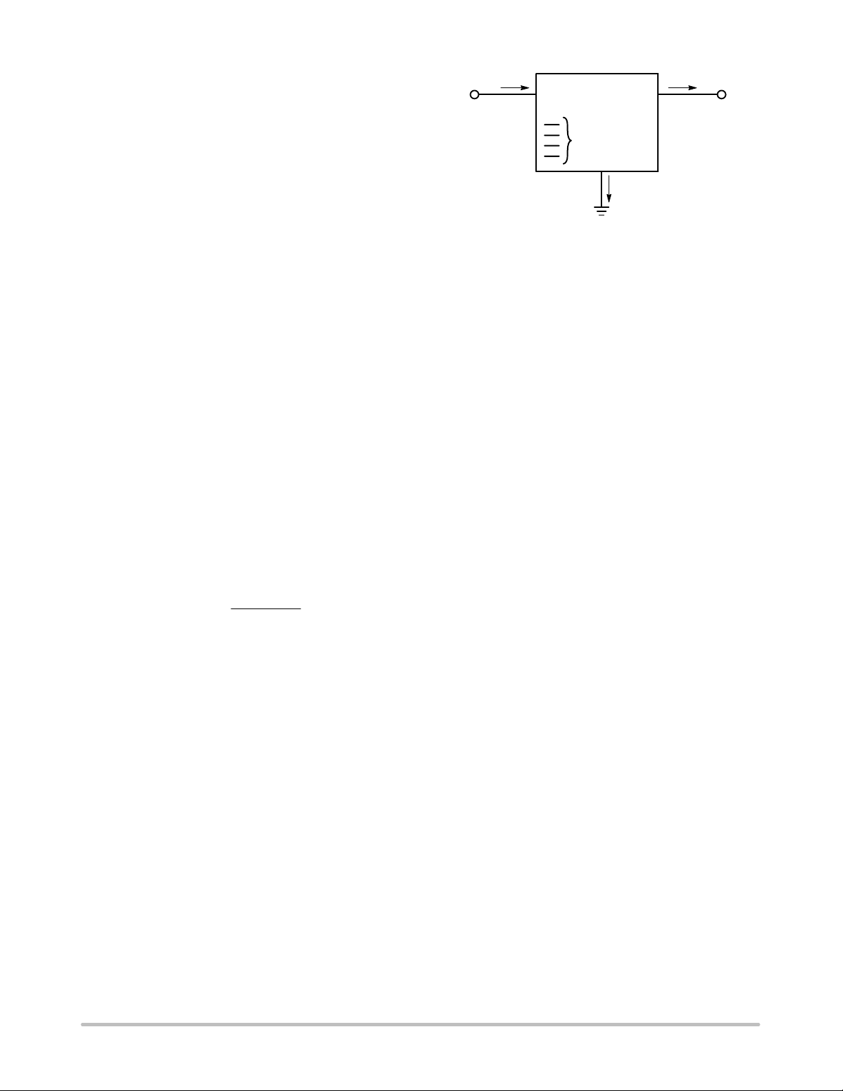
I
IN
V
IN
SMART
REGULATOR
Control
Features
I
Q
I
OUT
V
®
OUT
Figure 14. Single Output Regulator With Key
Performance Parameters Labeled
HEAT SINKS
A heat sink effectively increases the surface area of the
package to improve the flow of heat away from the IC and
into the surrounding air.
Each material in the heat flow path between the IC and the
outside environment will have a thermal resistance. Like
series electrical resistances, these resistances are summed to
determine the value of R
R
+ R
qJA
qJC
qJA
.
) R
qCS
) R
qSA
(3)
where:
R
= the junction−to−case thermal resistance,
qJC
R
= the case−to−heatsink thermal resistance, and
qCS
R
= the heatsink−to−ambient thermal resistance.
qSA
R
appears in the package section of the data sheet. Like
qJC
R
, it too is a function of package type. R
qJA
qCS
and R
qSA
are
functions of the package type, heatsink and the interface
between them. These values appear in heat sink data sheets
of heat sink manufacturers.
http://onsemi.com
7

CS8129
MARKING DIAGRAMS
SO−16 WB
16
CS8129
AWLYYWWG
1
A = Assembly Location
WL = Wafer Lot
YY, Y = Year
WW = Work Week
G = Pb−Free Package
AWLYWWG
1
CS
8129
TO−220 5−LEAD
CS8129
AWLYWWG
1
CS
8129
AWLYWWG
1
ORDERING INFORMATION
Device Package Shipping
CS8129YT5 TO−220*
CS8129YT5G TO−220*
CS8129YTHA5 TO−220*
CS8129YTHA5G TO−220*
CS8129YTVA5 TO−220*
CS8129YTVA5G TO−220*
CS8129YDW16 SO−16WB
CS8129YDW16G SO−16WB
CS8129YDWR16 SO−16WB
CS8129YDWR16G SO−16WB
†For information on tape and reel specifications, including part orientation and tape sizes, please refer to our Tape and Reel Packaging
Specifications Brochure, BRD8011/D.
STRAIGHT
STRAIGHT
(Pb−Free)
HORIZONTAL
50 Units / Rail
HORIZONTAL
(Pb−Free)
VERTICAL
VERTICAL
(Pb−Free)
47 Units / Rail
(Pb−Free)
1000 / Tape & Reel
(Pb−Free)
†
http://onsemi.com
8

−Q−
U
K
D
5 PL
B
B1
12345
0.356 (0.014) T
M
G
DETAIL A−A
A
M
Q
CS8129
PACKAGE DIMENSIONS
TO−220
CASE 314D−04
ISSUE F
SEATING
−T−
PLANE
C
E
L
J
H
B
B1
NOTES:
1. DIMENSIONING AND TOLERANCING PER ANSI
Y14.5M, 1982.
2. CONTROLLING DIMENSION: INCH.
3. DIMENSION D DOES NOT INCLUDE
INTERCONNECT BAR (DAMBAR) PROTRUSION.
DIMENSION D INCLUDING PROTRUSION SHALL
NOT EXCEED 10.92 (0.043) MAXIMUM.
DIM MIN MAX MIN MAX
A 0.572 0.613 14.529 15.570
B 0.390 0.415 9.906 10.541
B1 0.375 0.415 9.525 10.541
C 0.170 0.180 4.318 4.572
D 0.025 0.038 0.635 0.965
E 0.048 0.055 1.219 1.397
G 0.067 BSC 1.702 BSC
H 0.087 0.112 2.210 2.845
J 0.015 0.025 0.381 0.635
K 0.977 1.045 24.810 26.543
L 0.320 0.365 8.128 9.271
Q 0.140 0.153 3.556 3.886
U 0.105 0.117 2.667 2.972
MILLIMETERSINCHES
DETAIL A−A
http://onsemi.com
9

TO−220
−Q−
0.356 (0.014)
CS8129
PACKAGE DIMENSIONS
TVA SUFFIX
CASE 314K−01
ISSUE O
NOTES:
SEATING
−T−
PLANE
C
B
E
W
U
12345
A
L
F
K
M
D
5 PL
M
M
T
Q
G
J
S
R
1. DIMENSIONING AND TOLERANCING PER ANSI
Y14.5M, 1982.
2. CONTROLLING DIMENSION: INCH.
3. DIMENSION D DOES NOT INCLUDE
INTERCONNECT BAR (DAMBAR) PROTRUSION.
DIMENSION D INCLUDING PROTRUSION SHALL
NOT EXCEED 10.92 (0.043) MAXIMUM.
DIM MIN MAX MIN MAX
A 0.560 0.590 14.22 14.99
B 0.385 0.415 9.78 10.54
C 0.160 0.190 4.06 4.83
D 0.027 0.037 0.69 0.94
E 0.045 0.055 1.14 1.40
F 0.530 0.545 13.46 13.84
G 0.067 BSC 1.70 BSC
J 0.014 0.022 0.36 0.56
K 0.785 0.800 19.94 20.32
L 0.321 0.337 8.15 8.56
M 0.063 0.078 1.60 1.98
Q 0.146 0.156 3.71 3.96
R 0.271 0.321 6.88 8.15
S 0.146 0.196 3.71 4.98
U 0.460 0.475 11.68 12.07
W 55°°
MILLIMETERSINCHES
Q
U
D5X
0.014 (0.356) T
B
−P−
TO−220
THA SUFFIX
CASE 314A−03
ISSUE E
NOTES:
SEATING
−T−
PLANE
C
OPTIONAL
CHAMFER
A
G
E
L
F
K
J
5X
S
M
M
P
1. DIMENSIONING AND TOLERANCING PER ANSI
Y14.5M, 1982.
2. CONTROLLING DIMENSION: INCH.
3. DIMENSION D DOES NOT INCLUDE
INTERCONNECT BAR (DAMBAR) PROTRUSION.
DIMENSION D INCLUDING PROTRUSION SHALL
NOT EXCEED 0.043 (1.092) MAXIMUM.
INCHES
DIMAMIN MAX MIN MAX
0.572 0.613 14.529 15.570
B 0.390 0.415 9.906 10.541
C 0.170 0.180 4.318 4.572
D 0.025 0.038 0.635 0.965
E 0.048 0.055 1.219 1.397
F 0.570 0.585 14.478 14.859
G 0.067 BSC 1.702 BSC
J 0.015 0.025 0.381 0.635
K 0.730 0.745 18.542 18.923
L 0.320 0.365 8.128 9.271
Q 0.140 0.153 3.556 3.886
S 0.210 0.260 5.334 6.604
U 0.468 0.505 11.888 12.827
MILLIMETERS
http://onsemi.com
10

SO−16 WB
16 9
M
B
H8X
M
0.25
0.25 B
14X
CS8129
PACKAGE DIMENSIONS
CASE 751G−03
ISSUE C
NOTES:
1. DIMENSIONS ARE IN MILLIMETERS.
D
A
q
E
_
h X 45
81
B16X
M
S
A
T
B
S
A
SEATING
T
PLANE
C
e
A1
L
2. INTERPRET DIMENSIONS AND TOLERANCES
PER ASME Y14.5M, 1994.
3. DIMENSIONS D AND E DO NOT INLCUDE
MOLD PROTRUSION.
4. MAXIMUM MOLD PROTRUSION 0.15 PER SIDE.
5. DIMENSION B DOES NOT INCLUDE DAMBAR
PROTRUSION. ALLOWABLE DAMBAR
PROTRUSION SHALL BE 0.13 TOTAL IN
EXCESS OF THE B DIMENSION AT MAXIMUM
MATERIAL CONDITION.
MILLIMETERS
DIM MIN MAX
A 2.35 2.65
A1 0.10 0.25
B 0.35 0.49
C 0.23 0.32
D 10.15 10.45
E 7.40 7.60
e 1.27 BSC
H 10.05 10.55
h 0.25 0.75
L 0.50 0.90
q 0 7
__
PACKAGE THERMAL DATA
TO−220
Parameter
R
q
JC
R
q
JA
Typical 2.1 23 °C/W
Typical 50 105 °C/W
FIVE LEAD
SO−16WB Unit
SMART REGULATOR is a registered trademark of Semiconductor Components Industries, LLC (SCILLC).
ON Semiconductor and are registered trademarks of Semiconductor Components Industries, LLC (SCILLC). SCILLC reserves the right to make changes without further notice
to any products herein. SCILLC makes no warranty, representation or guarantee regarding the suitability of its products for any particular purpose, nor does SCILLC assume any liability
arising out of the application or use of any product or circuit, and specifically disclaims any and all liability, including without limitation special, consequential or incidental damages.
“Typical” parameters which may be provided in SCILLC data sheets and/or specifications can and do vary in different applications and actual performance may vary over time. All
operating parameters, including “Typicals” must be validated for each customer application by customer’s technical experts. SCILLC does not convey any license under its patent rights
nor the rights of others. SCILLC products are not designed, intended, or authorized for use as components in systems intended for surgical implant into the body, or other applications
intended to support or sustain life, or for any other application in which the failure of the SCILLC product could create a situation where personal injury or death may occur. Should
Buyer purchase or use SCILLC products for any such unintended or unauthorized application, Buyer shall indemnify and hold SCILLC and its officers, employees, subsidiaries, affiliates,
and distributors harmless against all claims, costs, damages, and expenses, and reasonable attorney fees arising out of, directly or indirectly, any claim of personal injury or death
associated with such unintended or unauthorized use, even if such claim alleges that SCILLC was negligent regarding the design or manufacture of the part. SCILLC is an Equal
Opportunity/Affirmative Action Employer. This literature is subject to all applicable copyright laws and is not for resale in any manner.
PUBLICATION ORDERING INFORMATION
LITERATURE FULFILLMENT:
Literature Distribution Center for ON Semiconductor
P.O. Box 5163, Denver, Colorado 80217 USA
Phone: 303−675−2175 or 800−344−3860 Toll Free USA/Canada
Fax: 303−675−2176 or 800−344−3867 Toll Free USA/Canada
Email: orderlit@onsemi.com
N. American Technical Support: 800−282−9855 Toll Free
USA/Canada
Europe, Middle East and Africa Technical Support:
Phone: 421 33 790 2910
Japan Customer Focus Center
Phone: 81−3−5773−3850
http://onsemi.com
11
ON Semiconductor Website: www.onsemi.com
Order Literature: http://www.onsemi.com/orderlit
For additional information, please contact your local
Sales Representative
CS8129/D
 Loading...