

Page 1
查询CS1112供应商
CS1112
Quad Power Output Driver
The CS1112 is a Power Output Driver. The IC incorporates four
protected DMOS low–side drivers designed to drive inductive and
resistive loads in an automotive environment. The outputs are
controlled by an 8–bit serial peripheral interface (SPI) or its associated
parallel input. Each output contains overcurrent protection, open load
detection, and inductive flyback clamps. The device is overvoltage
protected. Overcurrent and open load faults are reported over the SPI
port, and at the STATUS lead.
I/O Control
SPI communication is initiated by asserting CSB low. Data at the SI
lead is transferred on the rising edge of SCLK. The MSB is transferred
first. The outputs become active at the rising edge of CSB. Diagnostic
status bits are transferred out the SO lead at the falling edge of SCLK.
The SO lead is high impedance while CSB is high. An open drain
output, (STATUS) reports a fault (short to V
has occurred at one or more of the outputs.
Protection
Each output independently detects shorts to V
is “on” and open load/short to ground while the output is “off”. The
fault register will be set if a fault occurs at the output. The fault register
will be reset if the fault condition is removed from the output. The
fault data is latched when CSB is asserted low.
If an overcurrent condition or short circuit to V
output goes into a low duty cycle mode for the duration of the fault.
The outputs are disabled during an overvoltage or undervoltage
condition.
Features
• 4.0 MHz Serial Input Bus
• Parallel Input Control
• 1.0 Ω DMOS Drivers (typ)
• Power On Reset
• Internal Flyback Clamps
• Status Output
• Fault Protection
– 46 V Peak Transient
– Power Limiting
– Undervoltage
– Overvoltage
• Fault Reporting
– Open Load
– Short Circuit
• 8 Internally Fused Leads
, GND, or open load)
PWR
while the output
PWR
occurs, the
BATT
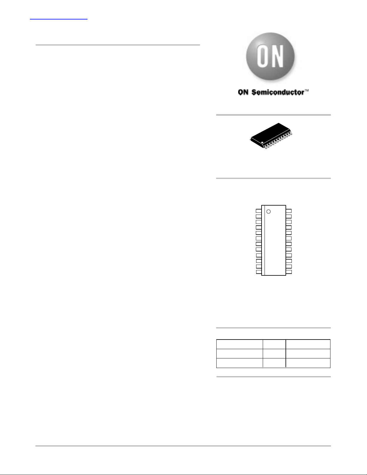
http://onsemi.com
SO–24L
DW SUFFIX
CASE 751E
PIN CONNECTIONS AND
MARKING DIAGRAM
1
V
DD
V
PWR
OUT0
IN0
GND
GND
GND
GND
IN1
OUT1
SI
CSB
A = Assembly Location
WL, L = Wafer Lot
YY, Y = Year
WW, W = Work Week
ORDERING INFORMATION
Device Package Shipping
CS1112YDWF24
CS1112YDWFR24
AWLYYWW
CS1112
SO–24L
SO–24L
24
R
OSC
STATUS
OUT3
IN3
GND
GND
GND
GND
IN2
OUT2
SO
SCLK
31 Units/Rail
1000 Tape & Reel
Semiconductor Components Industries, LLC, 2000
October, 2000 – Rev. 10
1 Publication Order Number:
CS1112/D
Page 2
CS1112
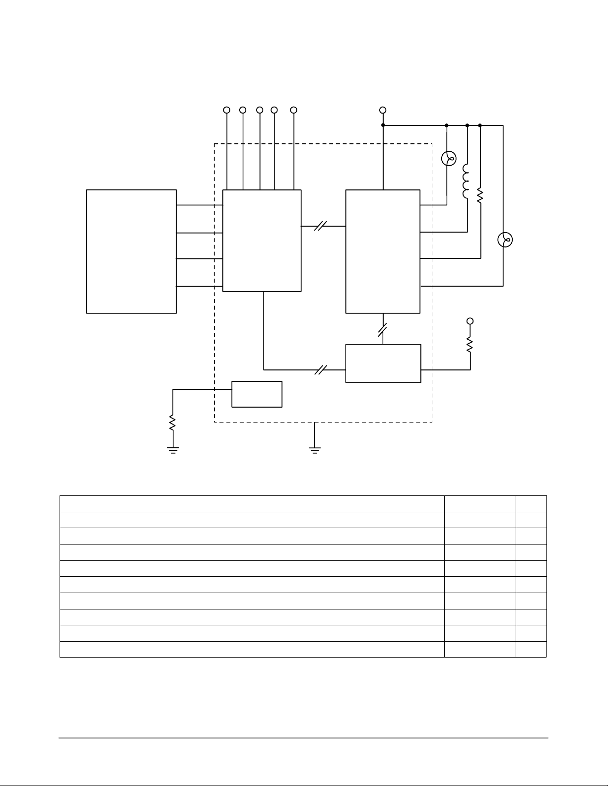
APPLICATION DIAGRAM
Micro Controller
with Bus
CSB
SCLK
R
OSC
IN1 IN2 IN3 IN4 V
SI
Registers and
SO
CMOS
Serial Shift
Latches
Bias
DD
QPOD
4
4
V
PWR
DMOS
Low Side
Switches and
Protection
Circuitry
4
Fault
Reporting
Status
V
DD
10 kΩ
R
OSC
82 kΩ
GND
ABSOLUTE MAXIMUM RATINGS*
Rating Value Unit
DC Supply (V
Output DC Voltage (Out 0, 1, 2, 3) 46 V
VDD Supply Voltage –0.3 to +7.0 V
Peak Transient (1.0 ms rise time, 300 ms period, 32 V Load Dump @ 14 V V
Digital Input Voltage –0.3 to VDD + 0.3 V
Single Pulse Avalanche Energy (I = 450 mA)(Out 0, 1, 2, 3) 50 mJ
Operating Junction Temperature, T
ESD Capability (Human Body Model) 1.5 kV
Lead Temperature Soldering: Reflow: (SMD styles only) (Note 1.) 230 peak °C
1. 60 second maximum above 183°C.
*The maximum package power dissipation must be observed.
) –0.3 to 30 V
PWR
) 46 V
PWR
J
–40 to 150 °C
http://onsemi.com
2
Page 3
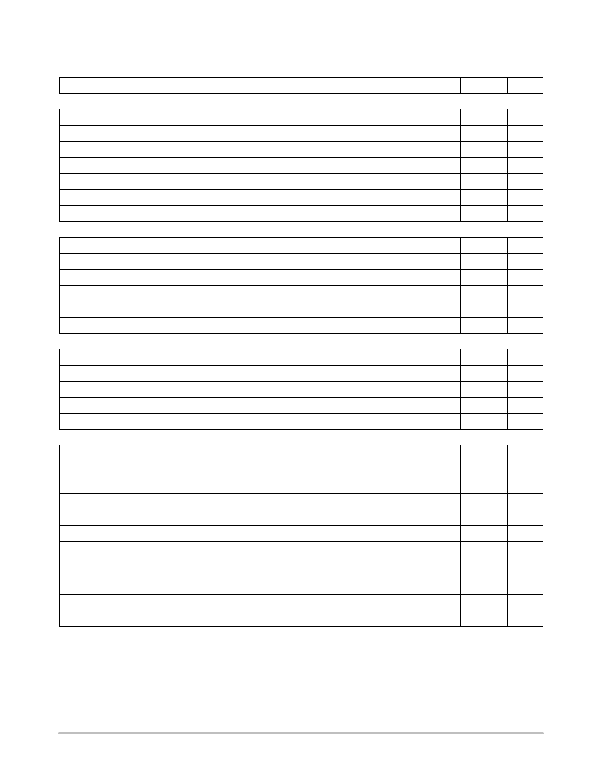
CS1112
ELECTRICAL CHARACTERISTICS (9.0 V < V
5.5
V < V
< 25 V, (Outputs Functional); unless otherwise specified.)
PWR
Characteristic
< 17 V, 4.5 V < VDD < 5.5 V, –40°C < T
PWR
Test Conditions Min Typ Max Unit
J <
125°C,
Supply Voltages and Currents
VDD Power On Reset Threshold Outputs Latched Off By Event 2.5 3.0 3.5 V
VDD Power On Reset Hysteresis – – 200 – mV
V
Undervoltage Outputs Latched Off By Event 4.0 4.5 5.0 V
PWR
V
Overvoltage Lockout Outputs Latched Off By Event 30 35 45 V
PWR
Digital Supply Current, I
Analog Supply Current, I
Sleep Current, I
V(PWR)
V(DD)
V(PWR)
All Outputs On (@ 350 mA) – – 5.0 mA
All Outputs On (@ 350 mA) – – 5.0 mA
VDD ≤ 0.5 V – – 10 µA
Digital Inputs and Outputs
VIN High SI, SCLK, CSB, IN0, IN1, IN2, IN3 70 – – %V
VIN Low SI, SCLK, CSB, IN0, IN1, IN2, IN3 – – 30 %V
VIN Hysteresis – – 230 – mV
Input Pulldown Current SI, IN0, IN1, IN2, IN3, VIN = 30% V
Input Pullup Current CSB, VIN = 70% V
Status Low I
= 0.5 mA – 0.1 0.5 V
STATUS
DD
DD
– – 25 µA
– – –25 µA
Fault Detection/Timing
Overcurrent Sense Time, t
SS
Overcurrent Shutdown Time Overcurrent Shutdown Time, R
Overcurrent Sense Time, R
= 82 kΩ 25 62.5 100 µs
OSC
= 82 kΩ 1.60 3.94 6.3
OSC
Fault Duty Cycle After the first fault cycle, Note 1. 1.4 1.56 1.7 %
Open Load Trip Point IN = Low 40 50 60 %V
Open Load Sense Time Open Load Sense Time, R
= 82 kΩ 12.5 – 100 µs
OSC
Power Outputs
V
Clamp ID = 20 mA, t
DRAIN
Drain Leakage Current V
Drain Leakage Current V
R
DS(ON)
= 17 V – – 25 µA
DRAIN
= 46 V – – 400 µA
DRAIN
V
= 13 V, ID = 0.5 A – 1.0 2.0 Ω
PWR
= 100 µs 48 52 64 V
CLAMP
Current Limit Note 2. 3.0 4.5 6.0 A
Reverse Diode Drop Reverse Diode Drop I = 350 mA – – 1.4 V
Fall Time Delay, t
phl
V
PWR
= 13 V, R
LOAD
= 33 Ω,
– – 10 µs
Note 3. (see Figure 2)
Rise Time Delay, t
plh
V
PWR
= 13 V, R
LOAD
= 33 Ω,
– – 15 µs
Note 3. (see Figure 2)
Rise Time, t
Fall Time, t
r
f
V
V
PWR
PWR
= 13 V, R
= 13 V, R
= 33 Ω 0.4 – 10 µs
LOAD
= 33 Ω 0.4 – 10 µs
LOAD
1. Guaranteed by design.
2. A duty cycle mode will initiate at a minimum of 1.0 A and before the current limit.
3. Output turn on delay and turn off delay from rising edge of CSB to the output reaching 50% of V
PWR
.
DD
DD
ms
DD
http://onsemi.com
3
Page 4
CS1112
ELECTRICAL CHARACTERISTICS (continued) (9.0 V < V
5.5
V < V
< 25 V, (Outputs Functional); unless otherwise specified.)
PWR
< 17 V, 4.5 V < VDD < 5.5 V, –40°C < T
PWR
J <
125°C,
Characteristic UnitMaxTypMinTest Conditions
Serial Peripheral Interface V
PWR
= 14 V
SCLK Clock Period CO = 200 pF 250 – – ns
MAX Input Capacitance SI, SCLK, Note 1. – – 12 pF
V
High SO, IOH = 1.0 mA VDD – 1.0 – – V
OUT
V
Low SO, IOL = 1.0 mA – – 0.5 V
OUT
SCLK High Time F
= 4.0 MHz, SCLK = 2.0 V to 2.0 V
SCLK
125 – – ns
(see Figure 1)
SCLK Low Time F
= 4.0 MHz, SCLK = 0.8 V to 0.8 V
SCLK
125 – – ns
(see Figure 1)
SI Setup Time SI = 0.8 V/2.0 V to SCLK = 2.0 V at 4.0 MHz;
25 – – ns
Note 1. (see Figure 1)
SI Hold Time SCLK = 2.0 V to SI = 0.8 V/2 .0 V at 4.0 MHz;
25 – – ns
Note 1. (see Figure 1)
SO Rise Time CLD = 200 pF (0.1 VDD to 0.9 VDD);
– 25 50 ns
Note 1.
SO Fall Time CLD = 200 pF (0.9 VDD to 0.1 VDD);
– – 50 ns
Note 1.
CSB Setup Time CSB = 0.8 V to SCLK = 2.0 V
60 – – ns
(see Figure 1) Note 1.
CSB Hold Time SCLK = 0.8 V to CSB = 2.0 V
75 – – ns
(see Figure 1) Note 1.
SO Delay Time SCLK = 0.8 V to SO Data Valid, VDD = 5.0 V
C
= 200 pF at 4.0 MHz
LD
– 65 125 ns
(see Figure 1); Note 1.
Xfer Delay Time CSB rising edge to next falling edge.
1.0 – – µs
Note 1.
1. Guaranteed by design.
PACKAGE PIN DESCRIPTION
PACKAGE PIN #
24 Lead SOIC
1 V
2 V
3 OUT0 Open drain output one.
4 IN0 Parallel input one.
5, 6, 7, 8
17, 18, 19, 20
9 IN1 Parallel input two.
10 OUT1 Open drain output two.
11 SI SPI serial input.
12 CSB SPI active low chip select.
13 SCLK SPI clock input.
14 SO SPI serial output.
PIN SYMBOL FUNCTION
DD
PWR
Input voltage to bias logic and control circuitry.
Input voltage to bias gate drive circuitry.
GND Ground Reference.
http://onsemi.com
4
Page 5

PACKAGE PIN DESCRIPTION (continued)
PACKAGE PIN #
24 Lead SOIC
15 OUT2 Open drain output three.
16 IN2 Parallel input three.
21 IN3 Parallel input four.
22 OUT3 Open drain output four.
23 STATUS Open drain output, which is asserted when an open load or
24 R
CS1112
overcurrent condition occurs at any of the outputs.
OSC
CIRCUIT DESCRIPTION
82 kΩ resistor tied to ground to set up accurate internal current sources.
FUNCTIONPIN SYMBOL
FUNCTIONPIN SYMBOL
Typical Operation
Control of the CS1112 can be done using the Serial
Peripheral Interface (SPI) port using the Data Input
information in Table 1, or the outputs can be controlled via
the parallel inputs (IN0, IN1, IN2, IN3). IN0 controls OUT0,
IN1 controls OUT1, IN2 controls OUT2, and IN3 controls
TIMING DIAGRAM
CS
SCLK
Don’t Care
SI
OUT3
OUT0
OUT1
Turn ON
OUT3. Turning the output drivers on is an OR function with
the SPI input and the parallel inputs.
Note: To prevent damage to the IC or the output load, V
DD
must be above the Power on Reset threshold (3.5 V) before
IN0, IN1, IN2, or IN3 are asserted high (< 70% VDD).
OUT2
Turn ON
OUT1
Turn OFF
OUT0
Turn ON
OUT2
OUT3
Time
Table 1. SPI Inputs
D7
X X X X OUT3 OUT2 OUT1 OUT0
MSB LSB
X = Don’t Care; MSB is Transferred first.
D6 D5 D4 D3 D2 D1 D0
http://onsemi.com
5
Page 6

CS1112
SERIAL PERIPHERAL INTERFACE TIMING REQUIREMENTS
CSB
SCLK
SI
SO
CSB (Setup)
CSB (Hold)
SI (Setup)
123
SI (Hold)
Xfer Delay
MSB
70% V
MSB
30% V
DD
DD
SO(Delay) SO(Rise,Fall)
Figure 1.
BLOCK DIAGRAM
IN0 IN1 IN2 IN3
CSB
OUT
t
f
t
phl
plh
t
r
X
t
Figure 2.
V
PWR
CSB
SI
SCLK
SO
V
DD
R
OSC
V
DD
10 µA
10 µA
Serial D/O
Line Driver
Power On
Reset
Bias
Serial
Peripheral
Interface
RESET
Data 0
Data 1 to 3
Fault 1 to 3
RESET
OUT
ENABLE
4.0 ms
Fault Timer
Overvoltage/
Undervoltage
Lockout
Fault 0
V
REG
Gate
Drive
Open Load
Data 0
Data 0
Shorted Load
I
LIMIT
OUT0
10 µA
OUT1
OUT2
OUT3
+
R
S
–
–
+
1/2 V
DD
GND
STATUS
http://onsemi.com
6
Page 7

CS1112
APPLICATION INFORMATION
CIRCUIT DESCRIPTION
The CS1112 was developed for use in very noisy and very
harsh environments such as seen in an automobile system.
The device has four low–side switches all controlled
through an 8–bit Serial Peripheral Interface (SPI) port.
Control of the outputs is also OR’d with parallel inputs. This
is a critical feature enhancement over similar devices
because of the ease in which the parallel inputs can be used
to control the outputs in a Pulse Width Modulation (PWM)
mode. Creating a PWM mode using just the serial port input
is not a practical application.
This part uses ON Semiconductor’s POWERSENSE
process technology. POWERSENSE combines the
robustness of Bipolar with the dense logic capability of
CMOS, and the power capabilities of DMOS.
Power consumption is kept to a minimum using
POWERSENSE in comparison to a bipolar technology. A
bipolar process requires DC bias currents to power–up the
integrated circuit. This is needed in many applications
requiring analog circuitry, but is not needed here. Digital
POWERSENSE logic dissipates power only when
switching because that is when transient gate charging
current flows. POWERSENSE logic requires little space,
and is a good economical solution. The DMOS side of the
process provides a robust user interface to the outside world
on each of the outputs. Peak transient capability of each
output is rated at a maximum of 46 V (typical of an
automotive load dump transient).
The CS1112 uses quasi–vertical DMOS transistors
resulting in an output resistance (R
) at each output of
DS(ON)
less than 1.0 Ω @ 13 V and 500 mA @ 25°C.
The part can be put in a sleep mode where the part draws
less than 2.0 µA of bias current from V
. The part enters
PWR
this sleep mode when VDD ≤ 0.5 V. Maximum quiescent
current for the device is 5.0 mA maximum for any
combination of output drivers enabled.
Fault reporting is controlled by the CS1112. Overcurrent
and short to V
are detected when the output is on. Open
BATT
load and short to ground are detected when the output is off.
Faults are reported out of the serial output (SO) pin as a new
8–bit word is being fed into the serial input (SI) pin.
Figure 3 highlights the SPI interface between the
microprocessor and the CS11 12. The SPI control inputs and
all other logic inputs are compatible with 5.0 V CMOS logic
levels.
Parallel
Inputs
µP
Receive Buffer
CS1112
SI
Shift Register
SO
SCLK
CSB
SPI Interface Fault Reporting
2103XXXX
3210
Output Logic
Figure 3.
Control
IN0
IN1
IN2
STATUS
µP
The four communication lines which define the SPI
interface are the SI, SO, CSB, and SCLK. The parallel
inputs, which control the outputs can also connect to the
same microprocessor, a separate microprocessor, or any
other sensor or electrical device which meets the voltage
requirements of the CS1112 (V
= VDD + 0.3 V).
IN(max)
SPI communication is as follows (2 scenarios):
1.
8–Bit Normal Operation
CSB pin is brought low activating the SPI port. Faults
detected since the last CSB low to high transition are
latched into the serial register when CSB goes low. 8
command bits are clocked into the SI pin. The four
fault bits are clocked out of the SO pin. CSB pin is
brought high translating the final 4 bits to the outputs
turning them on or off. Faults are then detected and
saved in the fault register when CSB goes low.
2.
16–Bit Operation For Command Verify
CSB pin is brought low activating the SPI port. 16 bits
are clocked into the SI pin (the last 4 are the 4 control
pins for the four outputs). CSB pin is brought high
translating the last 4 bits to the outputs turning them
on or off.
CSB pin is brought low activating the SPI port. 16
new bits are clocked into the SI pin. As the new bits
are being clocked in, the first 8 bits being clocked out
of the SO pin are the fault bits, followed by the first
8 bits which were clocked in (the verification bits).
The verification bits should replicate the command
bits.
http://onsemi.com
7
Page 8

CS1112
Serial clock frequencies up to 4.0 MHz can be used by the
CS1112.
Internal pull–up circuitry is provided on the Chip Select
Bar (CSB) pin. Internal active pulldowns are provided on the
parallel input pins (IN0, IN1, IN2, IN3, and SI pin).
A product highlight of this part is its ability to be
daisy–chained with other parts which follow the SPI
protocol as defined in Figure 1. Figure 4 displays this aspect.
The serial output of each device is fed into the serial input
of the next device. All data bits are clocked into their
respective registers, while the CSB pin is low. The drivers
are switched to the resulting command when the CSB pin is
brought back high.
µP
CSB SCLK
CS1112
SI
CSB SCLK CSB SCLK
Any IC using
SPI protocol
SO SI SO SI SO
Any IC using
SPI protocol
Figure 4.
Multiple SPI port devices can also be connected in a
parallel fashion (Figure 5) instead of the daisy–chained
connection previously shown. The microprocessor controls
the CS1112 in a multiplex fashion allowing the serial data
input to be input to the device when the device is activated
through the CSB pin. This creates a system whose number
of outputs is a multiple of 4. Figure 5 displays a 12 output
setup.
CS1112
SI
OUT0
SCLK
OUT1
CSB
µP
OUT2
OUT3
1 output with the SPI port, and 3 outputs being controlled
with the parallel inputs allowing them to run in a PWM
mode.
SPI Controlled Outputs
V
BAT
Z0 Z1 Z2 Z3
OUT0
OUT1
OUT2
µP
µP
SPI Port
Parallel Inputs
Control
SPI Port
CSB
SCLK
SI
IN0
IN1
IN2
CSB
SCLK
SI
OUT3
Figure 6.
Parallel Controlled Outputs
V
BAT
Z0 Z1 Z2 Z3
OUT0
OUT1
OUT2
OUT3
SPI Controlled
Outputs
CS1112
OUT0
SI
OUT1
SCLK
OUT2
CSB
OUT3
CS1112
OUT0
SI
OUT1
SCLK
CSB
OUT2
OUT3
Figure 5.
Figure 6 displays the device controlling 4 outputs with the
use of its SPI port. Figure 7 displays the device controlling
http://onsemi.com
Figure 7.
The CS1112 provides a very efficient way of controlling
4 output drivers by minimizing the number of I/O pins
through use of the SPI port, and still provides the flexibility
of pulse width modulating the output drivers where needed.
The use of the SPI also allows the integrated circuit to
communicate directly with the microprocessor.
While designed for an automotive environment, the
CS1112 can be used in other applications in the computer
market, industrial market, telecommunications market, or
any other instance where numerous drivers are needed. All
parts are 100% tested and guaranteed to meet all parameters
specified in the electrical characteristics. These
specifications cover the entire voltage range for V
(9.0 V to 17 V), and VDD (4.5 V to 5.5 V).
8
PWR
Page 9

CS1112
FAULT MODE OPERATION
The CS1112 provides protection for a multitude of system
faults and conditions. These include Overvoltage, Current
Limit, Open Circuit, Output Short to Power, Output Short to
Ground, and Flyback Clamp.
Overvoltage
The IC is constantly monitoring the voltage on the V
PWR
pin. If the voltage on this pin exceeds the Overvoltage
Shutdown Threshold (typically 35 V), all outputs
immediately turn off. The programmed outputs (via serial or
parallel input) turn back on once the voltage is brought back
down below this level.
Current Limit/Short to V
BATT
When the output current exceeds the Overcurrent (4.5 A
typical) for the Short Circuit/Overcurrent Sense Time
(typically 62.5 µs) as it would do during an output short to
V
, its fault status bit will be latched to a logic one. The
BATT
fault status bit remains latched until the rising edge of CSB.
The output will go into a low duty cycle mode (typically
1.56%) as long as the overcurrent condition exists, and the
channel is on. This protects the integrated circuit from
damaging itself due to its thermal limits.
Open Circuit/Short to Ground
Open circuit conditions are detected while the outputs are
off. A fault bit is set when the Open Load “Off” Detection
Voltage (typically 0.5 × V
) is present for the Open Load
DD
“Off” Sense Time (typically 62.5 µs) as it would do during
an output short to ground.
Flyback Clamp
While the flyback clamp is not a fault mode, it is a
protection feature of the CS1112. When driving inductive
loads, it is normal to observe high voltage spikes on the
output pin due to the stored energy in the windings when the
device is turned of f. On–chip clamps on the outputs limit the
voltage amplitude on the pin to prevent damage to the
device. Each output has an Output Clamp which limits the
output voltage to 52 V (typical when measured at 20 mA for
100 µs).
PIN FUNCTION DESCRIPTION
The signal on this pin is clocked from the falling edge of the
SCLK pin. The serial output data provides fault information
for each output and returns most significant bit (bit 7) first.
Bits 0 through 3 are output fault bits for outputs 0 through
3, respectively. In 8–bit SPI mode, bits 0–3, under normal
conditions return all zeros representing no faults. A 1
indicates a fault. The output from this pin conforms to
CMOS logic levels.
R
OSC
An 82 kΩ resistor tied to ground sets up an accurate
internal current source.
CSB
The CSB (Chip Select Bar) is the select pin when the
microprocessor wants to communicate with the CS1112. A
low on this pin enables the SPI communication with the
device and enables the SO pin. After the digital word is
clocked into the IC, a transition from low to high on the CSB
pin translates the last 4 bits of information turning the
outputs on or off. An internal active pull–up is connected to
this input. CMOS logic levels are required on this pin.
SCLK
The SCLK (Serial Clock) clocks the internal shift
registers. This pin controls the data being shifted into the SI
pin, and data being shifted out of the SO pin. CMOS logic
levels are required on this pin.
IN0, IN1, IN2, IN3
These pins control their corresponding numbered output.
These are the parallel input pins which may be used to PWM
the outputs. They have 230 mV of hysteresis. These inputs
are OR’d with their corresponding input bit in the serial
control byte. An internal active pull–down is connected to
these pins. CMOS logic levels are required on these pins.
OUT0, OUT1, OUT2, OUT3
These pins are the output low–side driver pins. They all
have typically 1.0 Ω R
DS(ON)
at V
= 13 V. Current limit
PWR
on these pins has a minimum specification of 3.0 A. A low
duty cycle mode (1.5% typ.) will initiate at a minimum of 1A
and before the current limit.
SI
The SI (Serial Input) receives serial 8–bit or 16–bit words
sent most significant bit first. Data is clocked in on the rising
edge of SCLK. An internal active pull–down is connected to
this input. CMOS logic levels are required on this pin.
SO
The SO (Serial Output) can be connected to the serial data
input pin of the microprocessor, or it can be daisy–chained
to the serial input (SI) of another SPI compatible device.
This pin is tri–stated unless a low CSB pin selects the device.
http://onsemi.com
V
PWR
14 V Battery voltage input. 5.0 mA (max) is needed.
V
DD
5.0 V Supply input. 5.0 mA (max) is needed.
STATUS
Open drain output. This pin goes low when an open load
or overcurrent condition occurs on any of the outputs. This
provides immediate notification to the controller that a fault
is present. The controller can subsequently query the device
(serially) to determine its origin.
9
Page 10

–T–
SEATING
PLANE
CS1112
PACKAGE DIMENSIONS
SO–24L
DW SUFFIX
CASE 751E–04
ISSUE E
–A–
1324
–B–
1
12
D24X
0.010 (0.25) B
M
S
A
T
S
12X
P
0.010 (0.25) B
M
J
M
F
R X 45
C
M
G22X
K
NOTES:
1. DIMENSIONING AND TOLERANCING PER ANSI
Y14.5M, 1982.
2. CONTROLLING DIMENSION: MILLIMETER.
3. DIMENSIONS A AND B DO NOT INCLUDE
MOLD PROTRUSION.
4. MAXIMUM MOLD PROTRUSION 0.15 (0.006)
PER SIDE.
5. DIMENSION D DOES NOT INCLUDE DAMBAR
PROTRUSION. ALLOWABLE DAMBAR
PROTRUSION SHALL BE 0.13 (0.005) TOTAL IN
EXCESS OF D DIMENSION AT MAXIMUM
MATERIAL CONDITION.
DIM MIN MAX MIN MAX
A 15.25 15.54 0.601 0.612
B 7.40 7.60 0.292 0.299
C 2.35 2.65 0.093 0.104
D 0.35 0.49 0.014 0.019
F 0.41 0.90 0.016 0.035
G 1.27 BSC 0.050 BSC
J 0.23 0.32 0.009 0.013
K 0.13 0.29 0.005 0.011
M 0 8 0 8
P 10.05 10.55 0.395 0.415
R 0.25 0.75 0.010 0.029
INCHESMILLIMETERS
PACKAGE THERMAL DATA
Parameter
R
Θ
JC
R
Θ
JA
SO–24L Unit
Typical 9 °C/W
Typical 55 °C/W
http://onsemi.com
10
Page 11

Notes
CS1112
http://onsemi.com
11
Page 12

CS1112
POWERSENSE is a trademark of Semiconductor Components Industries, LLC (SCILLC).
ON Semiconductor and are trademarks of Semiconductor Components Industries, LLC (SCILLC). SCILLC reserves the right to make changes
without further notice to any products herein. SCILLC makes no warranty, representation or guarantee regarding the suitability of its products for any particular
purpose, nor does SCILLC assume any liability arising out of the application or use of any product or circuit, and specifically disclaims any and all liability,
including without limitation special, consequential or incidental damages. “Typical” parameters which may be provided in SCILLC data sheets and/or
specifications can and do vary in different applications and actual performance may vary over time. All operating parameters, including “Typicals” must be
validated for each customer application by customer’s technical experts. SCILLC does not convey any license under its patent rights nor the rights of others.
SCILLC products are not designed, intended, or authorized for use as components in systems intended for surgical implant into the body, or other applications
intended to support or sustain life, or for any other application in which the failure of the SCILLC product could create a situation where personal injury or
death may occur. Should Buyer purchase or use SCILLC products for any such unintended or unauthorized application, Buyer shall indemnify and hold
SCILLC and its officers, employees, subsidiaries, affiliates, and distributors harmless against all claims, costs, damages, and expenses, and reasonable
attorney fees arising out of, directly or indirectly, any claim of personal injury or death associated with such unintended or unauthorized use, even if such claim
alleges that SCILLC was negligent regarding the design or manufacture of the part. SCILLC is an Equal Opportunity/Affirmative Action Employer.
PUBLICATION ORDERING INFORMATION
NORTH AMERICA Literature Fulfillment:
Literature Distribution Center for ON Semiconductor
P.O. Box 5163, Denver, Colorado 80217 USA
Phone: 303–675–2175 or 800–344–3860 Toll Free USA/Canada
Fax: 303–675–2176 or 800–344–3867 Toll Free USA/Canada
Email: ONlit@hibbertco.com
Fax Response Line: 303–675–2167 or 800–344–3810 Toll Free USA/Canada
N. American Technical Support: 800–282–9855 Toll Free USA/Canada
EUROPE: LDC for ON Semiconductor – European Support
German Phone: (+1) 303–308–7140 (Mon–Fri 2:30pm to 7:00pm CET)
Email: ONlit–german@hibbertco.com
French Phone: (+1) 303–308–7141 (Mon–Fri 2:00pm to 7:00pm CET)
Email: ONlit–french@hibbertco.com
English Phone: (+1) 303–308–7142 (Mon–Fri 12:00pm to 5:00pm GMT)
Email: ONlit@hibbertco.com
EUROPEAN TOLL–FREE ACCESS*: 00–800–4422–3781
*Available from Germany, France, Italy, UK, Ireland
CENTRAL/SOUTH AMERICA:
Spanish Phone: 303–308–7143 (Mon–Fri 8:00am to 5:00pm MST)
Email: ONlit–spanish@hibbertco.com
ASIA/PACIFIC: LDC for ON Semiconductor – Asia Support
Phone: 303–675–2121 (Tue–Fri 9:00am to 1:00pm, Hong Kong Time)
Toll Free from Hong Kong & Singapore:
001–800–4422–3781
Email: ONlit–asia@hibbertco.com
JAPAN: ON Semiconductor, Japan Customer Focus Center
4–32–1 Nishi–Gotanda, Shinagawa–ku, Tokyo, Japan 141–0031
Phone: 81–3–5740–2745
Email: r14525@onsemi.com
ON Semiconductor Website: http://onsemi.com
For additional information, please contact your local
Sales Representative.
http://onsemi.com
12
CS1112/D
 Loading...