CM1220
,
4 and 8-Channel ESD
Protection Arrays in CSP
Description
The CM1220 ESD protection arrays are available in four and eight
channel configurations. Each ESD channel features a nominal
capacitance of 14 pF making the devices ideal for protecting high
speed I/O ports and LCD and camera data lines without significantly
affecting signal integrity. The CM1220 integrates avalanche−type
ESD diodes on every channel, providing a very high level of
protection for sensitive electronic components that may be subjected
to electrostatic discharge (ESD). These diodes safely dissipate ESD
strikes of
IEC61000−4−2 international standard. Using the MIL−STD−883
(Method 3015) specification for Human Body Model (HBM) ESD, the
CM1220 protect against contact discharges at greater than
These devices are particularly well−suited for portable electronics
(e.g. wireless handsets, PDAs, notebook computers) because of their
small package and easy−to−use pin assignments. In particular, the
CM1220 is ideal for protecting high speed I/O ports and data and
control lines for the LCD display and camera interface in mobile
handsets.
The CM1220 incorporates ON Semiconductor’s OptiGuardt
coating for improved reliability at assembly in a space−saving,
low−profile Chip Scale Package.
Features
• Four and Eight Channels of ESD Protection
• OptiGuardtCoated for Improved Reliability
• ±15 kV ESD Protection on each Channel (IEC 61000−4−2 Level 4,
contact discharge)
• ±30 kV ESD Protection on each Channel (HBM)
• Chip Scale Package (CSP) Features Extremely Low Lead Inductance
for Optimum ESD Protection
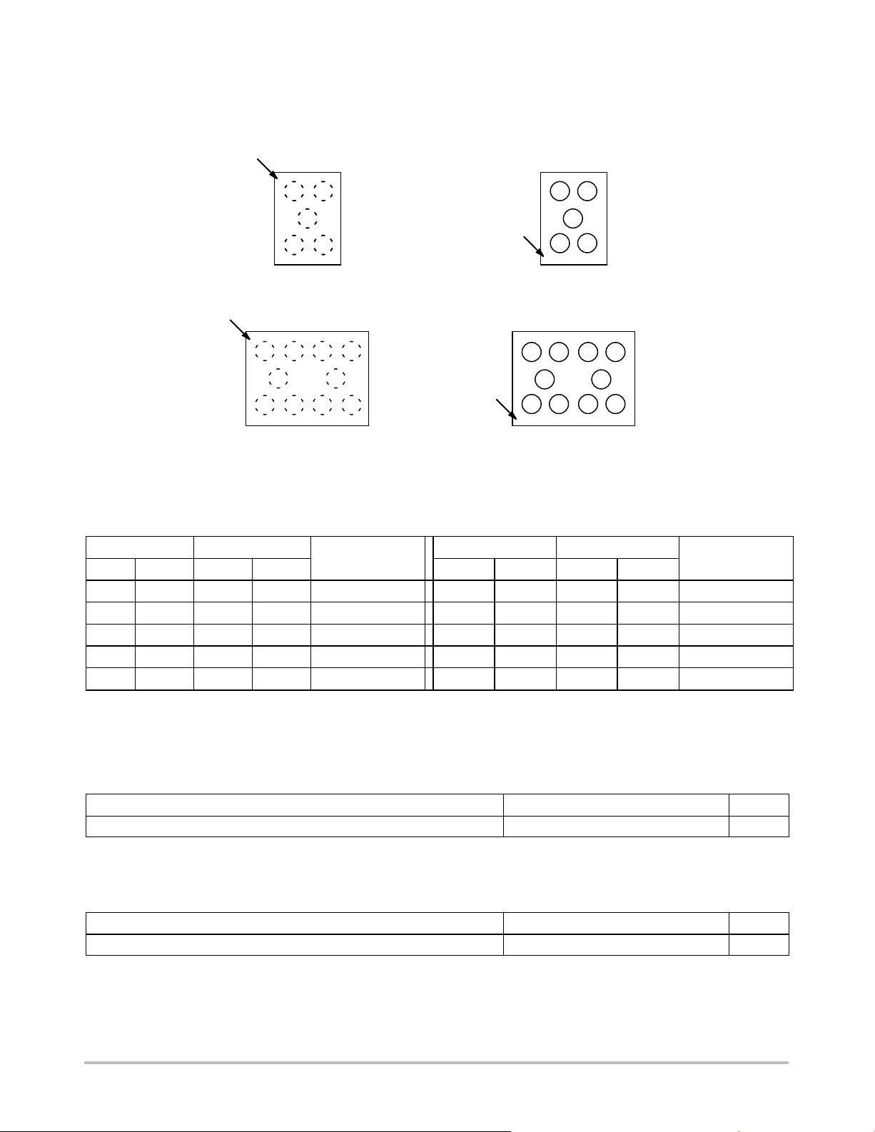
• 5 bump, 0.960 mm X 1.330 mm CSP Footprint for CM1220−04
• 10 bump, 1.960 mm X 1.330 mm CSP Footprint for CM1220−08
• These Devices are Pb−Free and are RoHS Compliant
Applications
• LCD and Camera Data Lines in Mobile Handsets
• I/O Port Protection for Mobile Handsets, Notebook Computers,
PDAs, etc.
• Keypads and Buttons
• Wireless Handsets
• Handheld PCs/PDAs
• LCD and Camera Modules
±15 kV, exceeding the maximum requirement of the
±30 kV.
http://onsemi.com
WLCSP5
CP SUFFIX
CASE 567AY
BLOCK DIAGRAM
ESD_1
A1
B2
GND
ESD_1
ESD_2
A1 A3 A5 A7
B1, B2
GND
J
CM1220−04
5−Bump CSP Package
J = CM1220−04CP
L208 = CM1220−08CP
ORDERING INFORMATION
Device Package Shipping
CM1220−04CP CSP−5
CM1220−08CP CSP−10
ESD_3
MARKING DIAGRAM
(Pb−Free)
(Pb−Free)
WLCSP10
CP SUFFIX
CASE 567BL
ESD_2
A3 C1
CM1220−04
ESD_4
CM1220−08
10−Bump CSP Package
ESD_3
ESD_4
C3
ESD_5
ESD_6
C1 C3 C5 C7
CM1220−08
3500/Tape & Reel
3500/Tape & Reel
ESD_7
L208
†
ESD_8
© Semiconductor Components Industries, LLC, 2011
February, 2011 − Rev. 3
†For information on tape and reel specifications,
including part orientation and tape sizes, please
refer to our Tape and Reel Packaging Specification
Brochure
1 Publication Order Number:
BRD8011/D.
CM1220/D

CM1220
PACKAGE / PINOUT DIAGRAMS
Bottom View
(Bumps Up View)
C1 C3
B2
A1 A3
A1
C1 C3
B2
A1 A3
A1
C5 C7
B6
A5 A7
Orientation
Marking
Orientation
Marking
Top View
(Bumps Down View)
+
A
B
C
123
+
A
B
C
L208
123
J
Orientation
Marking
CM1220−04
5−bump CSP Package
with OptiGuard
567
Orientation
Marking
CM1220−08
10−bump CSP Package
with OptiGuard
Table 1. PIN DESCRIPTIONS
CM1220−08 CM1220−04
Pins Name Pins Name Pins Name Pins Name
A1 ESD1 A1 ESD1 ESD Channel C1 ESD5 C1 ESD3 ESD Channel
A3 ESD2 A3 ESD2 ESD Channel C3 ESD6 C3 ESD4 ESD Channel
A5 ESD3 − − ESD Channel C5 ESD7 − − ESD Channel
A7 ESD4 − − ESD Channel C7 ESD8 − − ESD Channel
B2 GND B2 GND Device Ground B6 GND − − Device Ground
Description
CM1220−08 CM1220−04
Description
SPECIFICATIONS
Table 2. ABSOLUTE MAXIMUM RATINGS
Parameter Rating Units
Storage Temperature Range −65 to +150 °C
Stresses exceeding Maximum Ratings may damage the device. Maximum Ratings are stress ratings only. Functional operation above the
Recommended Operating Conditions is not implied. Extended exposure to stresses above the Recommended Operating Conditions may affect
device reliability.
Table 3. STANDARD OPERATING CONDITIONS
Parameter Rating Units
Operating Temperature Range −40 to +85 °C
http://onsemi.com
2

CM1220
Table 4. ELECTRICAL OPERATING CHARACTERISTICS (Note 1)
Symbol
C
DIODE
V
DIODE
I
LEAK
V
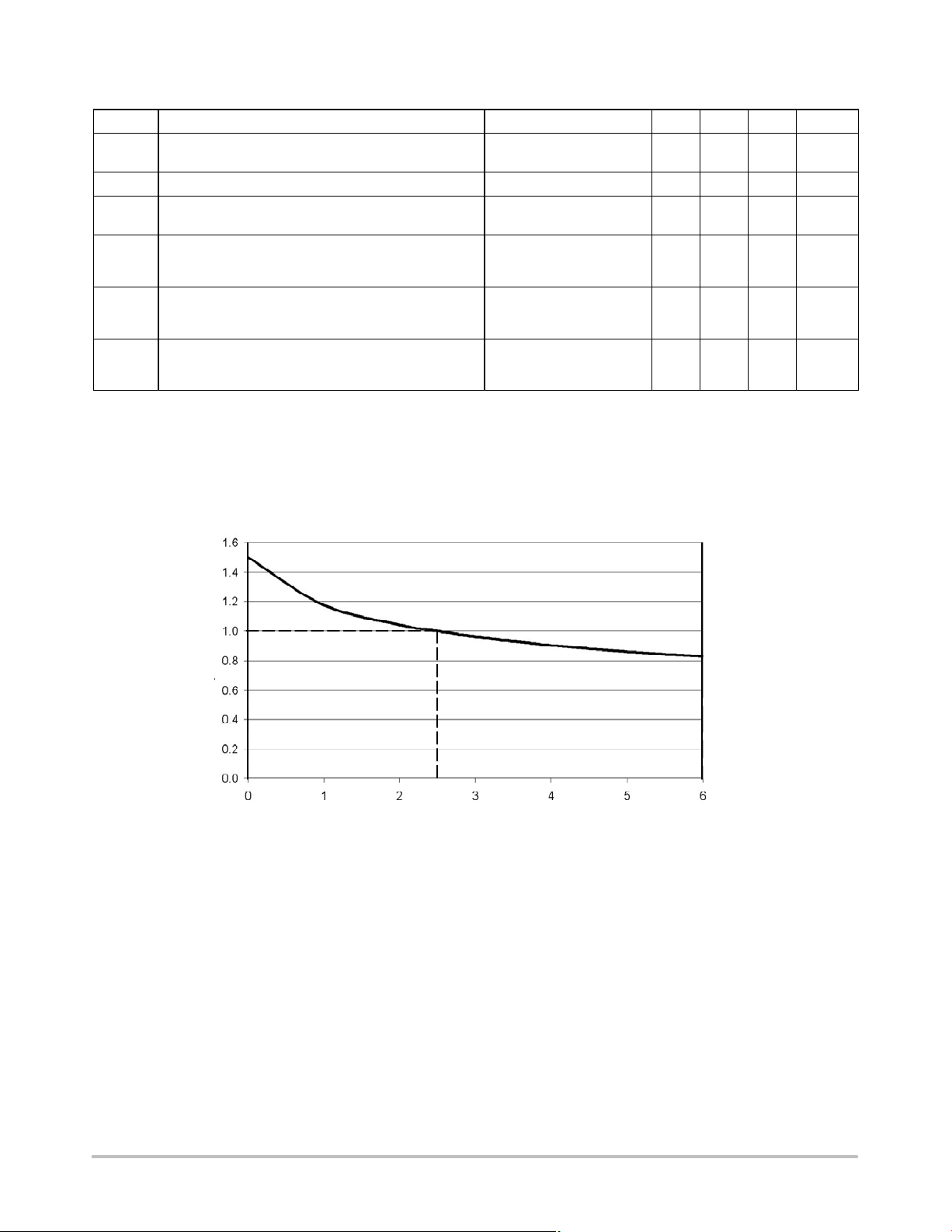
Diode (Channel) Capacitance At 2.5 VDC Reverse Bias,
Diode Standoff Voltage
Diode Leakage Current V
Signal Clamp Voltage
SIG
Positive Clamp
Negative Clamp
V
ESD
In−system ESD Withstand Voltage
a) Human Body Model, MIL−STD−883, Method 3015
b) Contact Discharge per IEC 61000−4−2
R
DYN
Dynamic Resistance
Positive
Negative
1. T
= 25 °C unless otherwise specified.
A
2. ESD applied to input and output pins with respect to GND, one at a time. Unused pins are left open.
Parameter Conditions Min Typ Max Units
1 MHz, 30 mVAC
I
= 10 mA
DIODE
= +3.3 V
IN
(reverse bias voltage)
I
= 10 mA
DIODE
(Note 2)
PERFORMANCE INFORMATION
11 14 17 pF
6.0 V
0.1 1
5.6
−1.5
6.8
−0.8
9.0
−0.4
±30
±15
2.3
0.9
mA
V
kV
W
Diode Characteristics (nominal conditions unless specified otherwise)
Capacitance (Normalized)
DC Voltage
Figure 1. Insertion Loss vs. Frequency (0 V Bias)
http://onsemi.com
3
 Loading...