

现货库存、技术资料、百科信息、热点资讯,精彩尽在鼎好!
BTA12-600BW3G,
BTA12-800BW3G
Triacs
Silicon Bidirectional Thyristors
Designed for high performance full−wave ac control applications
where high noise immunity and high commutating di/dt are required.
Features
• Blocking Voltage to 800 V
• On-State Current Rating of 12 A RMS at 25°C
• Uniform Gate Trigger Currents in Three Quadrants
• High Immunity to dV/dt − 2000 V/ms minimum at 125°C
• Minimizes Snubber Networks for Protection
• Industry Standard TO-220AB Package
• High Commutating dI/dt − 2.5 A/ms minimum at 125°C
• Internally Isolated (2500 V
• These are Pb−Free Devices
RMS
)
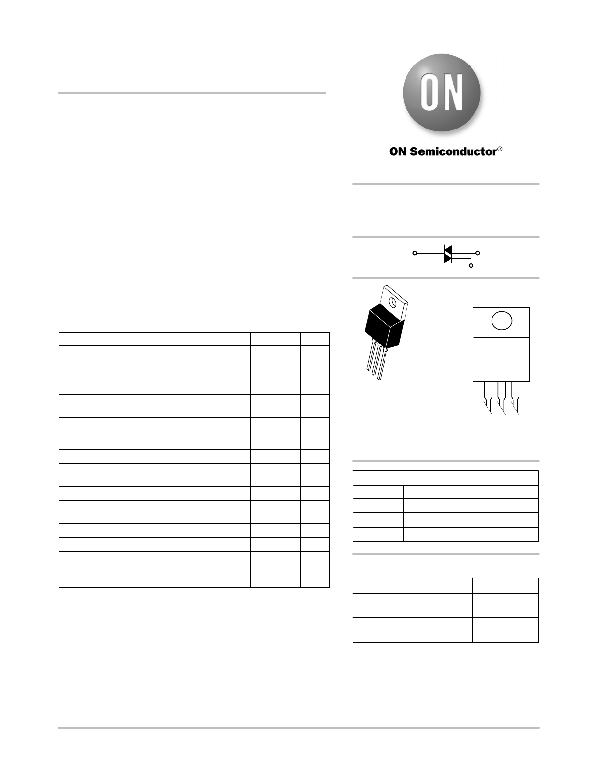
http://onsemi.com
TRIACS
12 AMPERES RMS
600 thru 800 VOLTS
MT2
4
MT1
G
MARKING
DIAGRAM
MAXIMUM RATINGS (T
Rating
Peak Repetitive Off−State Voltage (Note 1)
(T
= −40 to 125°C, Sine Wave,
J
50 to 60 Hz, Gate Open)
On-State RMS Current
(Full Cycle Sine Wave, 60 Hz, T
Peak Non-Repetitive Surge Current
(One Full Cycle Sine Wave, 60 Hz,
T
= 25°C)
C
Circuit Fusing Consideration (t = 8.3 ms) I2t 46 A2sec
Non−Repetitive Surge Peak Off−State
Voltage (T
Peak Gate Current (TJ = 125°C, t = 20ms) I
Peak Gate Power
(Pulse Width ≤ 1.0 ms, T
Average Gate Power (TJ = 125°C) P
Operating Junction Temperature Range T
Storage Temperature Range T
RMS Isolation Voltage
(t = 300 ms, R.H. ≤ 30%, T
Stresses exceeding Maximum Ratings may damage the device. Maximum
Ratings are stress ratings only. Functional operation above the Recommended
Operating Conditions is not implied. Extended exposure to stresses above the
Recommended Operating Conditions may affect device reliability.
1. V
voltages shall not be tested with a constant current source such that the
voltage ratings of the devices are exceeded.
= 25°C, t = 10ms)
J
and V
DRM
for all types can be applied on a continuous basis. Blocking
RRM
= 25°C unless otherwise noted)
J
Symbol Value Unit
V
DRM,
V
RRM
BTA12−600BW3G
BTA12−800BW3G
I
T(RMS)
I
TSM
V
DSM/
V
RSM
GM
P
GM
G(AV)
J
stg
V
iso
= 80°C)
C
= 25°C)
A
= 80°C)
C
600
800
12 A
105 A
V
DSM/VRSM
+100
4.0 A
20 W
1.0 W
−40 to +125 °C
−40 to +150 °C
2500 V
V
V
TO−220AB
1
2
3
x = 6 or 8
A = Assembly Location
Y = Year
WW = Work Week
G = Pb−Free Package
CASE 221A
STYLE 12
PIN ASSIGNMENT
1
2
3 Gate
4
Main Terminal 1
Main Terminal 2
No Connection
ORDERING INFORMATION
Device Package Shipping
BTA12−600BW3G TO−220AB
BTA12−800BW3G TO−220AB
(Pb−Free)
(Pb−Free)
BTA12−xBWG
AYWW
50 Units / Rail
50 Units / Rail
© Semiconductor Components Industries, LLC, 2008
August, 2008 − Rev. 0
*For additional information on our Pb−Free strategy and
soldering details, please download the ON Semiconductor Soldering and Mounting Techniques Reference
Manual, SOLDERRM/D.
1 Publication Order Number:
BTA12−600BW3/D
BTA12−600BW3G, BTA12−800BW3G
THERMAL CHARACTERISTICS
Characteristic Symbol Value Unit
Thermal Resistance, Junction−to−Case (AC)
Junction−to−Ambient
Maximum Lead Temperature for Soldering Purposes 1/8″ from Case for 10 seconds T
R
q
JC
R
q
JA
L
2.5
60
260 °C
°C/W
ELECTRICAL CHARACTERISTICS (T
= 25°C unless otherwise noted; Electricals apply in both directions)
J
Characteristic
OFF CHARACTERISTICS
Peak Repetitive Blocking Current
(VD = Rated V
DRM
, V
; Gate Open) TJ = 25°C
RRM
ON CHARACTERISTICS
Peak On-State Voltage (Note 2)
(ITM = ± 17 A Peak)
Gate Trigger Current (Continuous dc) (VD = 12 V, RL = 30 W)
MT2(+), G(+)
MT2(+), G(−)
MT2(−), G(−)
Holding Current
(V
= 12 V, Gate Open, Initiating Current = ±100 mA)
D
Latching Current (VD = 12 V, IG = 60 mA)
MT2(+), G(+)
MT2(+), G(−)
MT2(−), G(−)
Gate Trigger Voltage (VD = 12 V, RL = 30 W)
MT2(+), G(+)
MT2(+), G(−)
MT2(−), G(−)
Gate Non−Trigger Voltage (TJ = 125°C)
MT2(+), G(+)
MT2(+), G(−)
MT2(−), G(−)
DYNAMIC CHARACTERISTICS
Rate of Change of Commutating Current, See Figure 10.
(Gate Open, T
= 125°C, No Snubber)
J
Critical Rate of Rise of On−State Current
(T
= 125°C, f = 120 Hz, I
J
= 2 x IGT, tr ≤ 100 ns)
G
Critical Rate of Rise of Off-State Voltage
(V
= 0.66 x V
D
, Exponential Waveform, Gate Open, TJ = 125°C)
DRM
2. Indicates Pulse Test: Pulse Width ≤ 2.0 ms, Duty Cycle ≤ 2%.
= 125°C
T
J
Symbol Min Typ Max Unit
I
,
DRM
I
RRM
V
TM
I
GT
I
H
I
L
V
GT
V
GD
(dI/dt)
c
−
−
−
−
− − 1.55 V
2.5
2.5
2.5
−
−
−
− − 50 mA
−
−
−
0.5
0.5
0.5
0.2
0.2
0.2
−
−
−
−
−
−
−
−
−
2.5 − − A/ms
dI/dt − − 50
dV/dt 2000 − −
0.005
2.0
50
50
50
70
80
70
1.7
1.1
1.1
−
−
−
mA
mA
mA
V
V
A/ms
V/ms
http://onsemi.com
2
 Loading...