2N5038
NPN Silicon Transistors
Fast switching speeds and high current capacity ideally suit these
parts for use in switching regulators, inverters, wide-band amplifiers
and power oscillators in industrial and commercial applications.
Features
•High Speed - t
•High Current - I
•Low Saturation - V
= 0.5 ms (Max)
f
= 30 Amps
C(max)
= 2.5 V (Max) @ IC = 20 Amps
CE(sat)
•Pb-Free Package is Available*
MAXIMUM RATINGS (Note 1)
Rating Symbol Value Unit
Collector-Emitter Voltage V
Collector-Base Voltage V
Collector-Emitter Voltage V
Emitter-Base Voltage V
Collector Current - Continuous
Peak (Note 2)
Base Current - Continuous I
Total Device Dissipation @ TC = 25_C
Derate above 25_C
Operating and Storage Junction
Temperature Range
CEO
CBO
CEV
EBO
I
I
CM
P
TJ, T
C
B
D
stg
THERMAL CHARACTERISTICS
Characteristics Symbol Max Unit
Thermal Resistance, Junction-to-Case
Stresses exceeding Maximum Ratings may damage the device. Maximum
Ratings are stress ratings only. Functional operation above the Recommended
Operating Conditions is not implied. Extended exposure to stresses above the
Recommended Operating Conditions may affect device reliability.
1. Indicates JEDEC Registered Data.
2. Pulse Test: Pulse Width v 10 ms, Duty Cycle v 50%.
-65 to +200
R
q
JC
90 Vdc
150 Vdc
150 Vdc
7 Vdc
20
30
5 Adc
140
0.8
1.25
Adc
W
W/_C
_C
_C/W
http://onsemi.com
20 AMPERE
NPN SILICON
POWER TRANSISTORS
90 VOLTS - 140 WATTS
TO-204AA (TO-3)
CASE 1-07
STYLE 1
MARKING DIAGRAMS
2N5038G
AYYWW
MEX
2N5038
= 12 AMPS
I
C
I
= IB2 = 1.2 AMPS
B1
+11 V
0
-9 V
10 W
1N4933
-5 V
V
CC
+30 V
R
C
2.5
PW = 20 ms
DUTY CYCLE = 1%
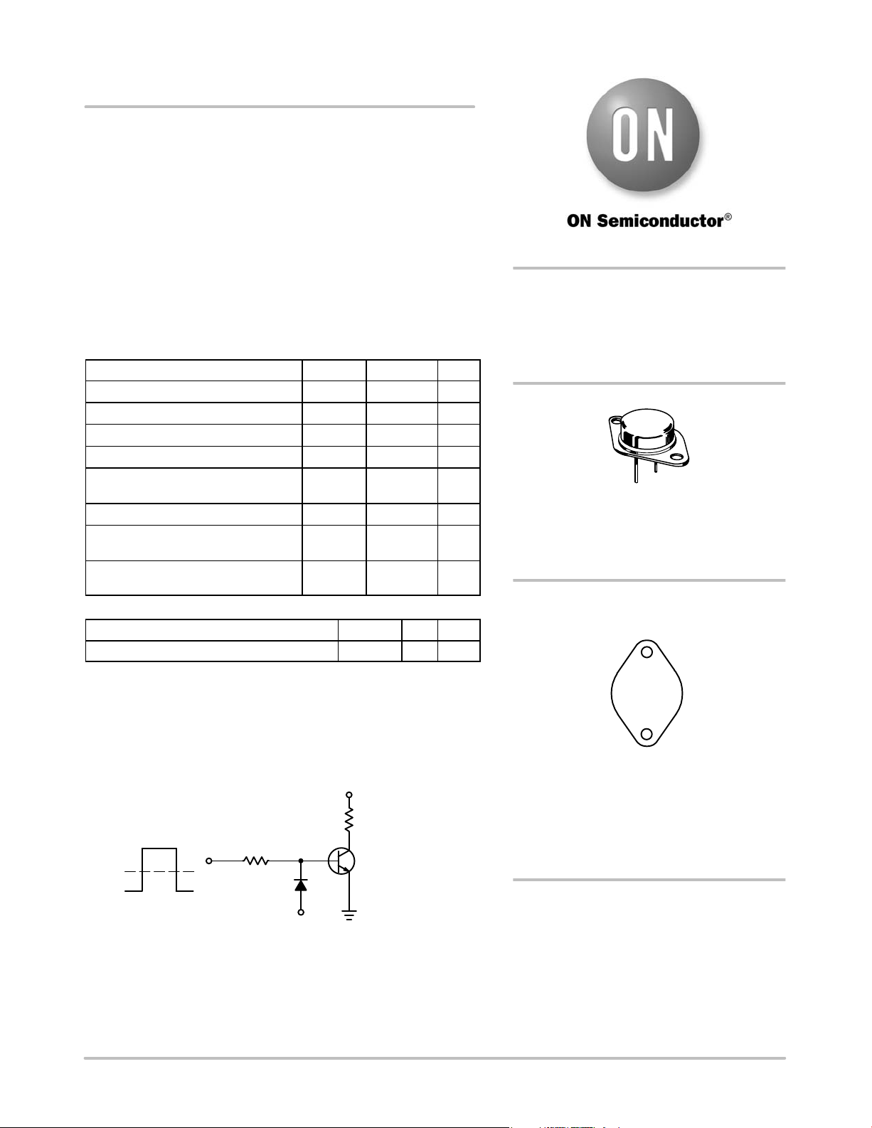
Figure 1. Switching Time Test Circuit
*For additional information on our Pb-Free strategy and soldering details, please
download the ON Semiconductor Soldering and Mounting Techniques
Reference Manual, SOLDERRM/D.
© Semiconductor Components Industries, LLC, 2007
August, 2007 - Rev. 12
1 Publication Order Number:
G = Pb-Free Package
A = Assembly Location
YY = Year
WW = Work Week
MEX = Country of Origin
ORDERING INFORMATION
See detailed ordering and shipping information in the package
dimensions section on page 2 of this data sheet.
2N5038/D

2N5038
ELECTRICAL CHARACTERISTICS (T
Characteristic
OFF CHARACTERISTICS
Collector-Emitter Sustaining Voltage (Note 4)
(I
= 200 mAdc, IB = 0)
C
Collector Cutoff Current
(V
= 140 Vdc, V
CE
= 100 Vdc, V
(V
CE
Emitter Cutoff Current
(V
= 5 Vdc, IC = 0)
EB
(VEB = 7 Vdc, IC = 0)
ON CHARACTERISTICS (Note 4)
DC Current Gain
(I
= 12 Adc, VCE = 5 Vdc)
C
Collector-Emitter Saturation Voltage
(I
= 20 Adc, IB = 5 Adc)
C
Base-Emitter Saturation Voltage
(I
= 20 Adc, IB = 5 Adc)
C
DYNAMIC CHARACTERISTICS
Magnitude of Common-Emitter Small-Signal Short-Circuit Forward Current Transfer
Ratio (I
SWITCHING CHARACTERISTICS
RESISTIVE LOAD
Rise Time
Storage Time
3. Indicates JEDEC Registered Data.
4. Pulse Test: Pulse Width v 300, ms, Duty Cycle v 2%.
= 2 Adc, VCE = 10 Vdc, f = 5 MHz)
C
= 1.5 V)
BE(off)
= 1.5 Vdc, TC = 150_C)
BE(off)
(VCC = 30 Vdc)
(IC = 12 Adc, IB1 = IB2 = 1.2 Adc)
= 25_C unless otherwise noted) (Note 3)
C
Symbol
V
CEO(sus)
I
CEX
I
EBO
h
FE
V
CE(sat)
V
BE(sat)
|hfe|
t
r
t
s
Min
90
-
-
-
-
20
-
-
12
-
-
Max
-
50
10
5
50
100
2.5
3.3
-
0.5
1.5
Unit
Vdc
mAdc
mAdc
-
Vdc
Vdc
-
ms
ms
ORDERING INFORMATION
Device Package Shipping
2N5038 TO-204
2N5038G TO-204
100
50
20
10
5
2
1
0.5
, COLLECTOR CURRENT (AMPS)
C
I
0.2
0.1
1 10 100
BONDING WIRE LIMIT
THERMAL LIMIT
SECOND BREAKDOWN LIMIT
TC = 25°C
2 3 5 7 20 30 50
VCE, COLLECTOR-EMITTER VOLTAGE (VOLTS)
dc
(Pb-Free)
70
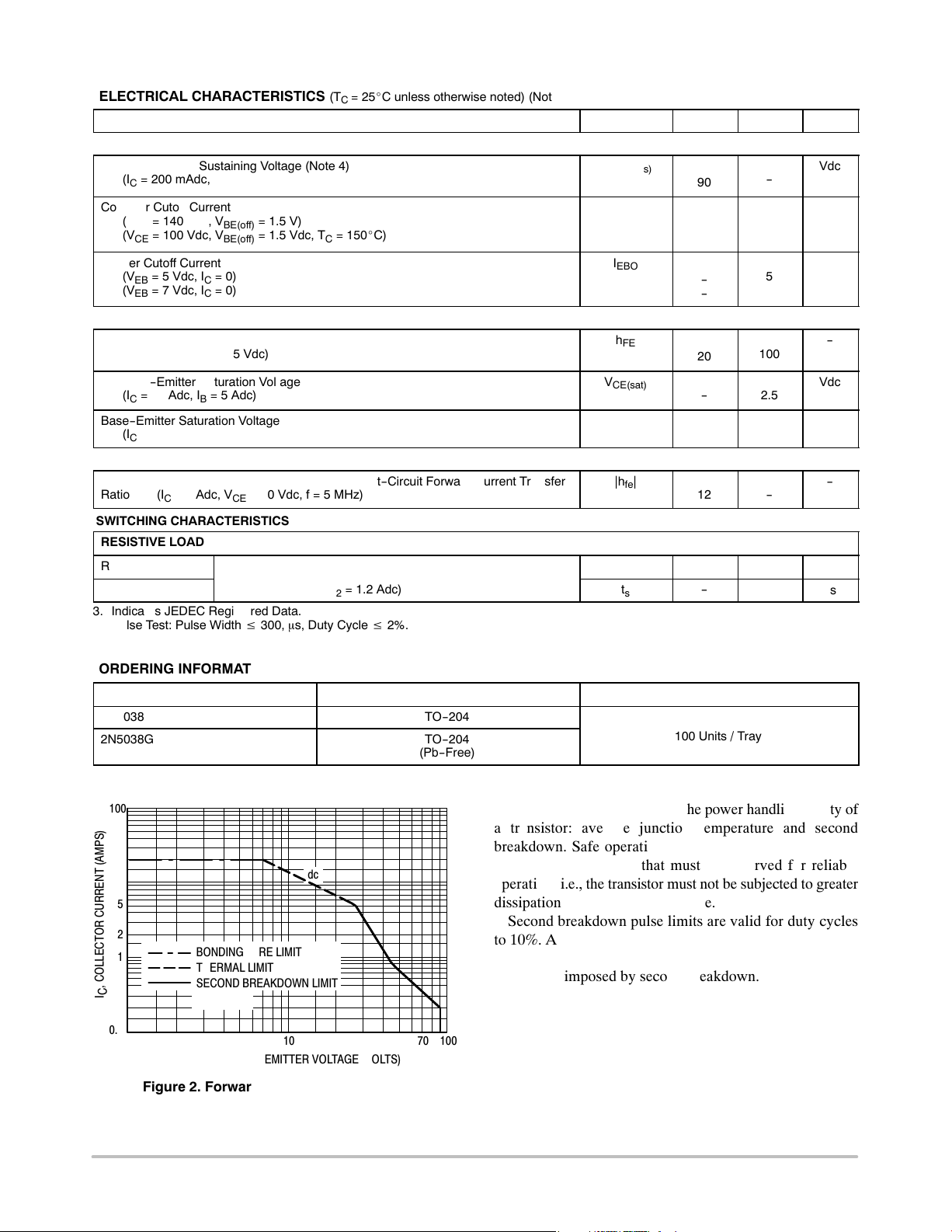
Figure 2. Forward Bias Safe Operating Area
100 Units / Tray
There are two limitations on the power handling ability of
a transistor: average junction temperature and second
breakdown. Safe operating area curves indicate I
- V
C
CE
limits of the transistor that must be observed for reliable
operation; i.e., the transistor must not be subjected to greater
dissipation than the curves indicate.
Second breakdown pulse limits are valid for duty cycles
to 10%. At high case temperatures, thermal limitations may
reduce the power that can be handled to values less than the
limitations imposed by second breakdown.
http://onsemi.com
2

2N5038
PACKAGE DIMENSIONS
CASE 1-07
TO-204AA (TO-3)
ISSUE Z
A
N
C
E
2 PLD
0.13 (0.005) Y
U
V
H
L
2
1
G
-T-
K
M
-Y-
B
T
SEATING
PLANE
M
Q
M
-Q-
0.13 (0.005) T
M
M
Y
NOTES:
1. DIMENSIONING AND TOLERANCING PER ANSI
Y14.5M, 1982.
2. CONTROLLING DIMENSION: INCH.
3. ALL RULES AND NOTES ASSOCIATED WITH
REFERENCED TO-204AA OUTLINE SHALL APPLY.
DIM MIN MAX MIN MAX
A 1.550 REF 39.37 REF
B --- 1.050 --- 26.67
C 0.250 0.335 6.35 8.51
D 0.038 0.043 0.97 1.09
E 0.055 0.070 1.40 1.77
G 0.430 BSC 10.92 BSC
H 0.215 BSC 5.46 BSC
K 0.440 0.480 11.18 12.19
L 0.665 BSC 16.89 BSC
N --- 0.830 --- 21.08
Q 0.151 0.165 3.84 4.19
U 1.187 BSC 30.15 BSC
V 0.131 0.188 3.33 4.77
STYLE 1:
PIN 1. BASE
2. EMITTER
CASE: COLLECTOR
MILLIMETERSINCHES
http://onsemi.com
3
 Loading...