Page 1

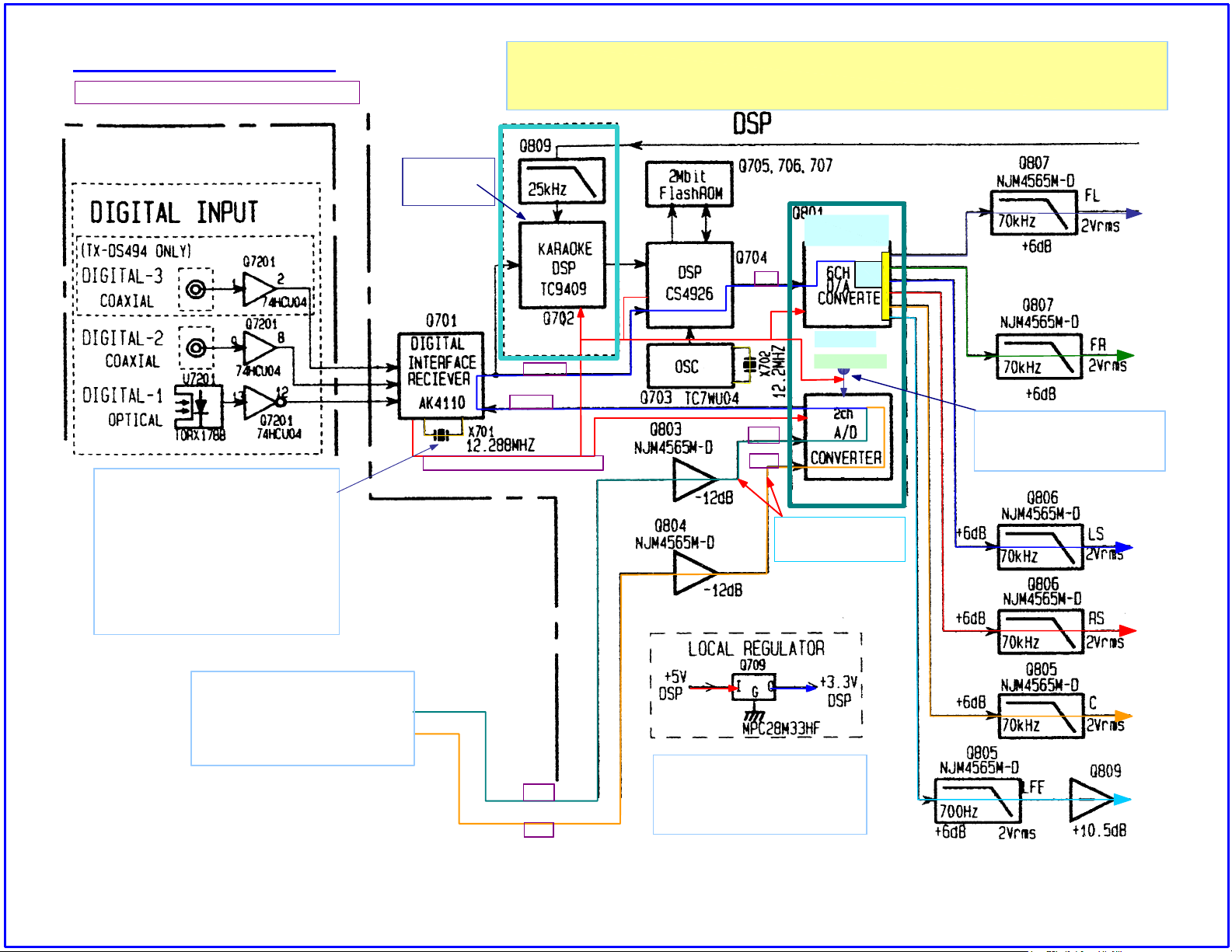
Based On TX-DS494
Analog signal processing method.
In many of the receivers X701 is turned ON
via control data, when source is analog
same IC often is utilized to perform the base
PLL frequency oscillation. L/R Clock
12,288mz/256= 48khz Q701 and its
surrounding components very easily
affected by to noise generated by power
supply or excessive grounding of the unit to
external devices. Always check and recheck
power supply regulators for least ripple or
H/F oscillation.
The most critical parts of the DSP besides the Base frequency oscillators, are the Flash-Rom's. These ROM's are often
configured in an 8-bit data bus mode, A failing or loose DSP Flash ROM's could trigger, data error in which DSP may
sound to break up and stutter do to mute ON-OFF. It may also mute indefinitely. It is recommended to check these
components very closely before assuming otherwise. Pins labeled A0~ and D0~ are often same DC level.
Does not
apply to US
models
L/R S/D
L/R S/D
L/R Clock 12,288mz/256= 48khz
Q801 DA/AD
Converter
S/D
AK4526A
Master Clock
Left
Right
Most DSP inputs are
configured in a
balanced input mode.
Q801 must have M/C and
Sampling frequency to work
properly. M/C is generated by
Q701 in most applications.
Input selector IC.
Analog source can be any of
the available inputs found on
the unit except multi-channel
input.
Left
Right
Most DSP design will incorporate a
local DC to DC regulator. It extremely
important to make sure the primary or
secondary DC have no H/F oscillation.
Page 1
 Loading...