

Page 1
SERVICE MANUAL
SERVICE MANUAL
STEREO CASSETTE TAPE DECK
MODEL TA-RW255
TA-RW255
Ref. No. 3872
062005
ONKYO
North American model
Other models
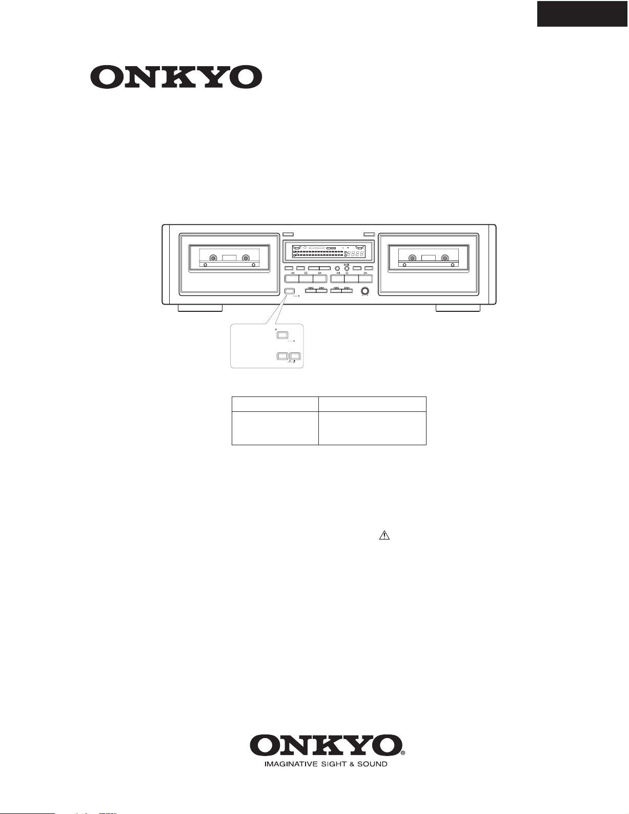
EJECT
DECK-A
PLAY
HI-SPEED DUBBING
L
dB -20- -10 -6 -3 +30+6
R
DOLBY NR
REVERCE MODE
POWER
STANDBY
STANDBY/ON
STANDBY
STANDBY/ON
MAIN POWER
OFF
ON
STANDBY
DOLBY NR
OFF B C
DUBBING COUNTER
AUTO SPACE
HIGHNORMAL A/B RESET
EJECT
DECK-B
PAUSE
PLAY
REC
A
B
DUBB.STOP
REC LEVEL
MIN MAX
Black and Silver models
BMDD
BMPA, BMGT
120V AC, 60Hz
230-240V AC, 50Hz
BMPP, SMPP
SAFETY-RELATED COMPONENT
WARNING!!
COMPONENTS IDENTIFIED BY MARK ON THE
SCHEMATIC DIAGRAM AND IN THE PARTS LIST ARE
CRITICAL FOR RISK OF FIRE AND ELECTRIC SHOCK.
REPLACE THESE COMPONENTS WITH ONKYO
PARTS WHOSE PART NUMBERS APPEAR AS SHOWN
IN THIS MANUAL.
MAKE LEAKAGE-CURRENT OR RESISTANCE
MEASUREMENTS TO DETERMINE THAT EXPOSED
PARTS ARE ACCEPTABLY INSULATED FROM THE
SUPPLY CIRCUIT BEFORE RETURNING THE
APPLIANCE TO THE CUSTOMER.
Page 2

SPECIFICATIONS
Format: Auto reverse double deck
Track format: 4-tracks, 2-channels
Recording system: AC bias
Erasing system: AC erase
Tape speed: 4.76 cm/sec. (1-7/8 i.p.s)
Wow and Futter: 0.13 % (WRMS)
Frequency response:
Metal position tape 30 Hz to 15 kHz ±3 dB
High position tape 30 Hz to 14 kHz ±3 dB
Normal position tape
Signal to noise ratio: 56 dB (metal position tape/ Type IV,
Input Jacks:
LINE IN: 2
Input sensitivity: 80 mV
Input impedance: 50 k ohm
Output Jacks:
LINE OUT: 2
Standard output level:
Output load impedance:
Motors: DC servo motor: 1+1
Heads:
PB Head: Special Hard Permalloy x 1
Rec/PB Head: Special Hard Permalloy x 1
Erase head: Ferrite x 1
Power supply rating: North American: AC 120 V, 60 Hz
Power consumption: 17 W
Standby power consumption:
Dimensions: (W x H x D):
Weight: 4.9 kg (10.8 lbs.)
Operation condition temperature/humidity:
30 Hz to 13 kHz ±3 dB
Dolby NR off)
55 dB (high position/ Type II, Dolby NR
off)
50 dB (normal position/ Type I, Dolby
NR off)
Noise reduction of 10 dB above 5 kHz
and 5 dB at 1 kHz possible with Dolby B.
Noise reduction of 20 dB at 5 kHz
possible with Dolby C.
500 mV
over 50 k ohm
European: AC 230 - 240 V, 50 Hz
North American: 7.0 W
European: 0.6 W
435 mm x 121 mm x 303 mm
(17-1/8" x 4-3/4" x 11-15/16")
5 C - 35 C/ 5% - 85% (no condensation)
TA-RW255
Specifications and external appearance are subject to change
without notice because of product improvements.
Page 3
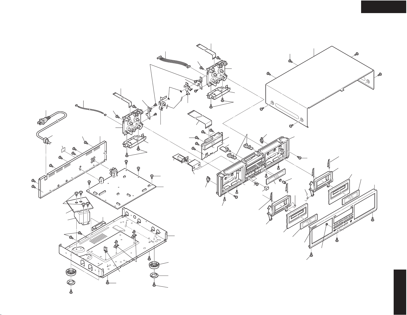
TA-RW255
EXPLODED VIEW
P101
P901A
A202
A026 A201
A208
x 7 pcs.
P801
A029
x 2 pcs.
Z001
Z009
x 4 pcs.
Z005
P102
Z008
x 2 pcs.
Z003
A010
A011
x 2 pcs.
Z006
Z007
x 2 pcs.
A029
x 5 pcs.
U05
A029
x 4 pcs.
U01
A029
x 2 pcs.
Z004
P701
A204
A007
P802
Z002
A010
A011
x 2 pcs.
U02
U04
A008
x 2 pcs.
A205
A203
A007
A006
A302
x 6 pcs.
A001
A021
A016
A015
A301
A004
x 2 pcs.
A014
x 2 pcs.
A013
A316
A317
A305
A028
x 4 pcs.
U03
T901
A029
x 2 pcs.
A020
E851
A206
x 2 pcs.
A019
x 2 pcs.
A017
A311
x 4 pcs.
A313
x 8 pcs.
A312
x 4 pcs.
A003
x 4 pcs.
A014
x 2 pcs.
A013
A315
A317
A308
A306
x 3 pcs.
A307
Except
<MDD>
TA-RW255
Page 4
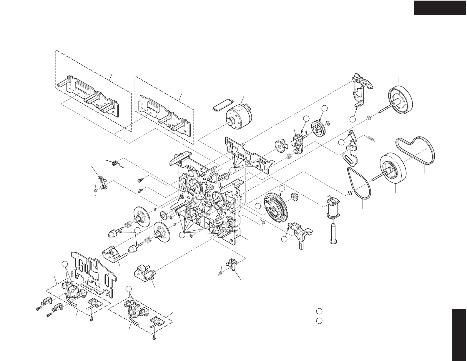
TA-RW255
EXPLODED VIEW
F567-750
F REC
CMAL2Z226B
Lever for prevent to lever.
(only Left side mecha.)
METAL
PACK
05a
Cr
R REC
CASSETTE MECHANISM
Z001 : CMAL2Z226B (PLAY Deck)
Z002 : CMAL2Z227B (REC/PLAY Deck)
F567-739
05b
PACK
Cr
04
A
A
30
A
A
06
A
A
A
25
29
42
F513-930
A
B
32
B
03a
03b
31
A
F513-931
02
CMAL2Z227B
Lever for prevent to eject
(Both mecha.)
A
: MOLYKOTE EM-60L : CORNING
A
: SCREW LOCK : BOND
B
TA-RW255
Page 5
CASSETTE MECHA. PARTS LIST
TA-RW255
No.
03a
03b
04
05a
05b
06
25
29
30
31
32
42
PART No.
F513-931
F513-930
F525-382
F567-739
F567-750
F522-063
FF19N
FR26D-11
FR26B-21
F514-133
F514-134
FF19S
PART NAME
PLATE HEADD BLOCK
PLATE HEADD BLOCK
MOTOR MAIN BLOCK
PCB CONTROL BLOCK
PCB CONTROL BLOCK
CLUTCH ASSY BLOCK
MAIN BELT
ASSY F/W
ASSY F/W
ROLLER PINCH BLOCK R
ROLLER PINCH BLOCK L
F/R BELT
NOTE
226B
227B
226B
227B
F/W Material: ES-5
F/W Material: ES-5 x 2
Page 6
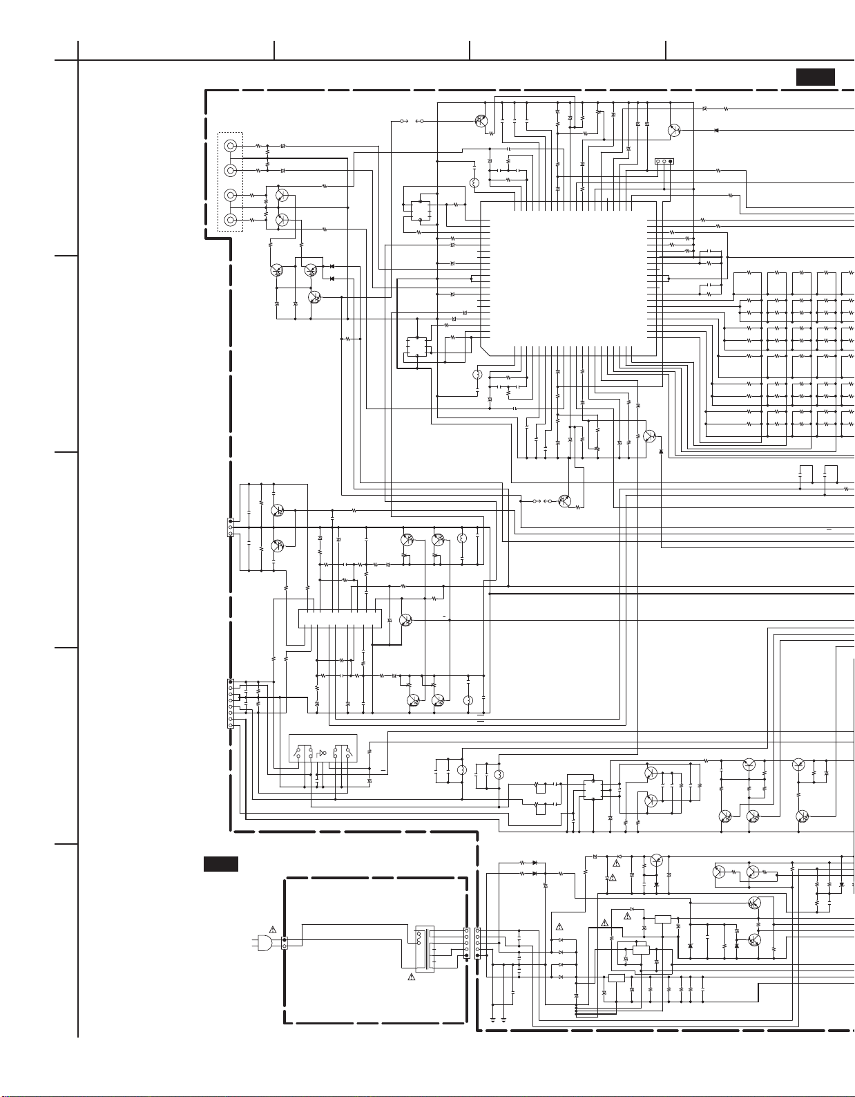
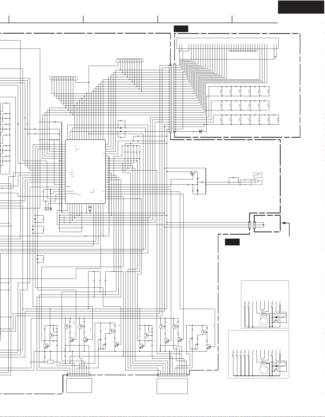
SCHEMATIC
DIAGRAM
<MDD> ONLY
A
1
2
3
4
5
BCDEFGH
BIAS_CTRL
BIAS_NORM
BIAS_H
DECK_B_70/120
DECK_A_70/120
LINE_MUTE
PB_X1/X2
LINE_MUTE
REC/PB
+5V
+12VM
+12VA
-17V
DECK_B/A
A:H/B:L
LCHRCH
A_PB_LCH B_PB_LCH
B_PB_RCH
A_PB_RCH
NAPS-8557
Alternative use C904 or C916.
R405
4.7
R406
4.7
Q407
2SC1959
C105
681
C106
681
R103
100K
R104
100K
C109
333
R109
100K
R111
3.3K
C113
681
R113
3.9K
C111
153
R115
10K
R108
3.9K
C110
333
R110
100K
C112
153
R112
3.3K
C114
681
R116
10K
C123
470/16
+
C126
101
R910
5.6K
R911
5.6K
D601
1SS352
D602
1SS352
R114
3.9K
R224
10K
R220
100K
R214
560
C216
222
C218
104
C220
104
C210
222
R212
22K
C214
104
R229
12K
R211
22K
C211
222
R213
560
C213
104
C219
104
C217
104
C215
222
C209
222
R227
12K
R260
180K
R261
68K
R262
1M
R263
100K
R264
100K
R265
120K
R266
220K
R267
220K
R268
120K
R269
NC
R270
220K
R271
47K
R272
1M
R273
47K
R274
NC
R275
150K
R276
120K
R277
NC
R278
330K
R279
330K
R280
220K
R281
33K
R282
330K
R283
47K
R284
150K
R285
33K
R286
100K
R287
1M
R288
82K
R289
NC
R290
82K
R291
33K
R292
330K
R293
33K
R295
82K
R296
120K
R297
NC
R298
180K
R299
NC
R294
220K
R300
82K
R301
47K
R302
47K
R303
33K
R304
NC
R305
100K
R306
150K
R307
NC
R308
220K
R309
NC
R727
470
C712
104
R751
R416
5.6K
R122
100(1/2W)
R121
4.7K
Q604
KRA107S
R107
3.9K
R408
39K
C404 472
Q406
2SC1959
R415
47K
R410
1K
R414
2.2K
R413
10K
R407
39K
C403 472
Q401
2SB1068
Q403
2SC1959
C206
1/50
+
C205
1/50
+
R231
18K
R241
3.3K
R242
3.3K
R243
6.8K
R244
6.8K
R215
4.7K
R217
3.3K
C223
1/50
+
R216
4.7K
R218
3.3K
C224
1/50
+
C228
2.2/50
+
C227
2.2/50
+
R417
100(1/2W)
Q603
KRA107S
R409
10(1/2W)
R411
820
C406
183
C241
1/50
+
C602
470/16
+
C601
1/50
+
C208
10/16
+
R201
22K
R202
22K
R203
68K
L203
NCH2137
2 1
R228
12K
C229
4.7/50
+
R222
10K
R221
10K
C230
4.7/50
+
R230
12K
C232
4.7/50
+
C231
4.7/50
+
D201
1SS352
D202
1SS352
Q203
RN1411
Q408 uPC1330HA
123
4
CNT
5
GND6VCC
789
L201
NMC6079
3
2
176
5
4
8
L202
NMC6079
6
5
4
8
3
2
1
7
C102
221
R101
100K
C101
221
R102
100K
C104
471
C103
471
C707
104
C918
2.2/50
+
R914
2.2K
R915
2.2K
R909
2.7K
C932
104
R725
22K
Q706
2SD655
R724
22K
Q705
2SD655
R728
0
C911
273
C212
222
C238
331
C237
331
C407
123/100V
C402
101
L403
NLO-2059
3
2
1
8
6
5
4
7
R404
100KB
123
R403
100KB
123
R119
50KB
2
13
R117
50KB
2
13
R118
50KB
2
31
R120
50KB
2
31
Q101 BA3416BL
13579
111315
17
1816141210
864
2
R237
56K
R238
47K
R240
100K
R239
100K
R245
10K
C236
104
C235
104
P205
321
C125
101
C401
101
C409
223
D703
UDZS5.6B
C405 223
R903
3.9K
C914
104
R912
2.2K
R913
2.2K
Q903
78M05
1
I
2
G
3
O
Q901
78M12
1
I
2
G
3
O
R923
10(1/2W)
D907
UDZS18C
D904 1N4003
2 1
D9031N4003
2 1
D902 1N4003
2 1
D9011N4003
2 1
D913
1N4003
2 1
C915
1/50
+
Q904
2SA933S
C910
2200/16
+
P102A
8
7
6
5
4
3
2
1
P101A
1
2
3
L401
4.7mH
NCH2133
2 1
C413
681
C415
680
C414
681
C416
680
Q902
7812
1
I
4
2
G
5
3
O
D911
1SS352
D905
1N4003
1 2
R924
680
R925
680
R926
680
D923
1SS352
D924
1SS352
C923
22/50
R902
1(1/2W)
C912
10/50
+
C913
47/50
+
D906
1N4003
21
Q906
KRA107S
R726
470
R723
22K
Q201
HA12169FB
61
VREF2
62
NRIN2
63
IAOUT2
64
BIAS
65
RPI2
66
VRI32
67
VRI22
68
CONT2
69
VRI12
70
GND22
71
GND11
72
VRI11
73
CONT1
74
VRI21
75
VRI31
76
RPI1
77
REF1
78
IAOUT1
79
NRIN1
80
VREF1
1
BIASTRAP12PBOUT13SS114SS215CCR16HLS17LLS18RECOUT19LMIN1
10
LMDET111LMOUT112EQIN113EQCONT114IREF15EQOUT116NN17NH18NM19HN20HH
21
HM
22
GP
23
GL
24
GH
25
F/Q
26
FQ
27
FM
28
BIASCONT1
29
DACOUT1
30
VCC
31
VCC
32
DACOUT2
33
BIASCONT2
34
GND
35
BIASADJN
36
BIASADJM
37
BIASADJH
38
INJ
39
CLK
40
DATA
41
STB
42
RESET
43
MPX
44
C/B
45
NRONOFF
46
EQOUT2
47
DGND
48
EQCONT2
49
EQIN2
50
LMOUT2
51
LMDET2
52
LMIN2
53
RECOUT2
54
LLS2
55
HLS2
56
CCR2
57
SS2258SS12
59
PBOUT2
60
BIASTRAP2
R236
47K
R235
3.3K
R105
33
R106
33
C108
470/6.3
+
R226
20KB
1
2
3
R123
560
R223
10K
R225
20KB
2
1 3
R219
100K
C128
223
Q204
RN1411
L204
NCH2137
1 2
C764
223
C763
223
R753
3.3K
R601
2.2K
R232
0
R233
0
R234
0
C127
104
C233
0.1/50
+
C919
100/25
+
R314
56
R313
56
R204
68K
J2A
1
J2B
1
J1A
1
J1B
1
E002 E001
C903
104
C907
104
C934
223
Q102
KRC107S
Q103
KRC107S
Q104
KRC107S
Q905
KRC107S
Q404
KRC107S
Q605
KRC107S
Q105
KRC107S
Q402
KRC107S
Q405
KRC107S
Q107
KRC107S
Q108
KRC107S
Q206
KRC107S
Q205
KRC107S
C107
470/6.3
+
C115
10/50
+
C116
10/50
+
C122
10/50
+
C121
22/50
+
C202
10/50
+
C201
10/50
+
C203
10/50
+
C204
10/50
+
C207
10/50
+
C221
100/25
+
C222
100/25
+
C226
10/50
+
C225
10/50
+
C239
10/50
+
C240
10/50
+
C408
10/50
+
C410
22/50
+
C411
220/25
+
C905
10/50
+
C906
100/25
+
C908
220/25
+
C909
10/50
+
P201
2
1
3
5
4
6
JL902A
5
4
3
2
1
JL902B
1
2
3
4
5
T901
NPT-1523D
6
5
2 15
14
NC
13
12
NC
11
10
9
D910
UDZS5.6B
L101
NCH2137
1 2
C117
331
L402
4.7mH
NCH2133
2 1
P901
2
1
P901A
C118
331
Q106
KRC107S
L102
NCH2137
2
1
R206
1K
R205
1K
R207
6.8K
R208
6.8K
Q602
2SD655
Q601
2SD655
R315
100
R316
100
R209
2.2K
R210
2.2K
R125
470
R126
470
R127
470
R128
470
C904
13000/25
+
U01 MAIN PC BOARD NAAF-8555
U03
POWER SUPPLY PC BOARD
NC
NC
NC
NC
NC
NC
DECK A
DECK B
Page 7
TA-RW255
P-OFF
RESET
SOL_A_ON/OFF
CAP_A_X1/X2
CAP_A_ON/OFF
CAP_B_X1/X2
SOL_B
CAP_B
REC_MUTE
SIG_L
SIG_RCH
1G
4G
P15
P10P9P8P7P6P5P4P3P2
P1
1G2G3G
4G
P15
P14
P13
P12
P11
P10
P9
P8
P7
P6
P5
P4
P3
P2
P1
1G
2G
3G
4G
KEY0
KEY1
KEY2
HIGH SW
PACK SW
REC INH FWD
FM
FQ
F/Q
GH
GL
GP
N.NORMN.HIGHN.MTLH.NORMH.HIGHH.MTL
HIGH SPEED
NORM SPEED
NORM SPEED
HIGH SPEED
TEST_MODE
DECK A
REC INH REV
METAL SW
MOTOR +
MOTOR B
MOTOR A
ROT PH DIODE
MOTER -
FT
PACK SW
HIGH SW
MOTER -
ROT PH DIODE
MOTOR A
MOTOR B
MOTOR +
PLAY SW
ROT PH OUT A
SOLENOID
ROT PH OUT B
SOLENOID
PLAY SW
DECK B
NAAF-8555
F-PLAY R-PLAY DOLBY_NRREWFFSTOP
DECK_B
STOP B-FF B-REW B_F-PLAY B_R-PLAY REV_MODE
STBY
ON/OFF
REC_PAUSE
AUTO_SPACE
NORM_DUBB
HIGH_DUBB
COUNTER
RESET
COUNTER
A/B
DECK_A
NADIS-8556
NAETC-8558
INPUT VR
BA-+
MOTOR
DECK B
BA-+
MOTOR
SOL
SOL
DECK A
OTP ONLY
OTP ONLY
7
+5V SENSOR
6
MOTOR A5MOTOR B
8
MOTOR- COM
9
HIGH SW
10
PACK SW
11
REC INH FWD
12
REC INH REV
13
METAL SW
4
MOTOR+
3
PLAY SW
2
ROT PHT OUT
1
SOLENOID
7
+5V SENSOR
6
MOTOR A5MOTOR B
4
MOTOR+
3
PLAY SW
2
ROT PHT OUT
1
SOLENOID
8
MOTOR- COM
9
HIGH SW
10
PACK SW
R823
3.9K
R825
3.9K
R826
18K
C804
223
R250
100K
R251
56K
R252
NC
R253
56K
R254
NC
R255
56K
R256
82K
R257
NC
R258
100K
R259
NC
R260
180K
R261
68K
R262
1M
R263
100K
R264
100K
R265
120K
R266
220K
R267
220K
R268
120K
R269
NC
R751
100K
Q809 2SB1068
R822
47K
R824
47K
R829
1M
R817
2KB
2
3 1
R820
100K
Q812
2SA933S
R807
47K
R808
3.9K
R809
47K
Q805 2SB1068
R810
3.9K
R812
18K
C803
223
R831
1M
R772
180(1/2W)
R805
100K
R802
2KB
2
3 1
Q801
2SB1068
Q804
2SA933S
Q813
2SB1068
R733
2.7K
R734
2.7K
R735
2.7K
R742
4.7K
R738
4.7K
P5021
2
3
C722
104Z
C721
104Z
Q702
KRA107S
D701
1SS352
R748
470
R747
220K
R781100KX10
11
10
987654321
R783
0
R745
4.7K
D704
1SS352
R830
10K
Q815
2SA1037AK
R828
10K
Q807
2SA1037AK
R786
0
L701
BK1608LM182-T
D702
UDZS5.6B
D703
UDZS5.6B
R782 100KX10
123456789
10
11
R791
0
D708
1SS352
D707
1SS352
R792
0
R793
0
P705
1
2
3
D709
1SS352
D801
1N4003
2
1
D802
1N4003
2 1
R731
4.7K
R732
4.7K
R744
4.7K
R743
4.7K
R741
4.7K
R739
4.7K
R740
4.7K
R797
10K
R798
0
P701A
1
2
3
4
5
6
7
8
9
10
11
12
13
14
15
16
17
18
19
20
21
22
23
24
25
26
27
28
29
R746
47K
P801A
123456789
10
R737
4.7K
Q703
78L05
1I3
O
2
G
P702A
1
2
3
R813
47K
R827
47K
P802A
12345678910111213
R801
6.8K
R816
6.8K
R803
1KB
2
3 1
R818
1KB
2
3 1
R821
10K
R806
10K
R311
10K
R312
10K
R753
3.3K
R754
3.3K
R310
10K
Q701
MPD78042FGF
1
CAP_A
2
CAP_A_X2/X1
3
SOL_A
4
1G
5
2G
6
3G
7
4G
8
VDD
9
DOL_CLK
10
DOL_DATA
11
DOL_STB
12
DOL_RST
13
A_70/120
14
B_70/120
15
PB_X1/X2
16
LINE_MUTE
17
RESET
18
REC MUTE
19
P-OFF
20
AVSS
21
FT_MODE
22
TEST_MODE
23
SIG_LCH
24
SIG_RCH
25
VOL
26
KEY227KEY1
28
KEY029AVDD
30
AVREF
31
XT1/GND32XT2/NC
33
VSS34X135X2
36
BIAS_CONT37N.BIAS38H.BIAS39R/P
40
B/A
41
R.SEN_B
42
R.SEN_A
43
CAP_B
44
CAP_B_X1/X2
45
SOL_B
46
RI_OUT
47
RI_IN
48
IC(VPP)GND
49
A_PACK_SW
50
A_HIGH_SW
51
A_PLY_SW
52
VDD
53
B_PLY_SW
54
B_HIGH_SW
55
B_PACK_SW
56
B_F.REC_INH
57
B_MTL_SW
58
B_R.REC_INH
59
NC
60
SRCH_OFF/ON
61
P16
62
P15
63
P14
64
P13
65
P1266P1167P10
68P969P870P771
VDISP
72P673P574P475P376P277P178
RELAY
79
S_LED
80
FL
R771
2.2K
R721
4.7K
R722
4.7K
R749
1K
C725
22/50
R819
1K
R804
1K
Q811
KRC107S
Q806
KRC107S
Q808
KRC107S
Q803
KRC107S
Q802
KRC107S
Q810
KRC107S
Q814
KRC107S
Q816
KRC107S
C761
10/50
+
C762
10/50
+
X701
CSTLS5M00
R736
NC
R752
3.3K
C765
223
S704
S705
S708
S710
S711
S712
S713
S714
S715
S716
S717
S719
S718
R702
470
R703
820
R7041KR705
1.8K
R706
390
R707
470
R708
820
R7091KR710
1.8K
R711
390
R712
470
R713
820
R7141KR715
1.8K
S702S709
R701
390
S703
R716
3.9K
S720
S706
S701
R717
3.9K
D706
SLI-343URC-TE7
Q707 BJ246GK
1
F112F125P176P167P158P149P13
10
P1211P1112P1013P914P815P716P617P518P419P320P221P122NC23NC24NC25NC26NC27NC28NC29NC30NC31NC32NC33NC34NC351G362G373G384G41F2142F22
P701B
1
2
3
4
5
6
7
8
9
10
11
12
13
14
15
16
17
18
19
20
21
22
23
24
25
26
27
28
29
R761
20KB
2
1
3
P702B
3
2
1
C723
104
C724
223
THE COMPONENTS IDENTIFIED BY MARK ARE CRITICAL FOR SAFETY.
REPLACE ONLY WITH PART NUMBER SPECIFIED.
VOLTAGE (MEASURED WITH VOLTMETER) IS DC VOLTAGE. (NO INPUT SIGNAL)
ELECTROLYTIC CAPACITORS ARE IN uF/WV.
ALL CAPACITORS ARE IN pF/50WV UNLESS OTHERWISE NOTED.
EX) 030 3pF 330 33pF 331 330pF 333 0.033uF
ALL RESISTORS ARE IN OHMS 1/4WATTS UNLESS OTHERWISE NOTED.
THE THICK LINES ON PC BOARD ARE THE PRINTING SIDE OF THE PARTS.
EX) PRINTING SIDE
CIRCUIT IS SUBJECT TO CHANGE FOR IMPROVEMENT.
NOTE
( )
NAAF-8555
U02
DISPLAY CIRCUIT PC BOARD
NADIS-8556
U04
INPUT VOLUME
PC BOARD
NAETC-8558
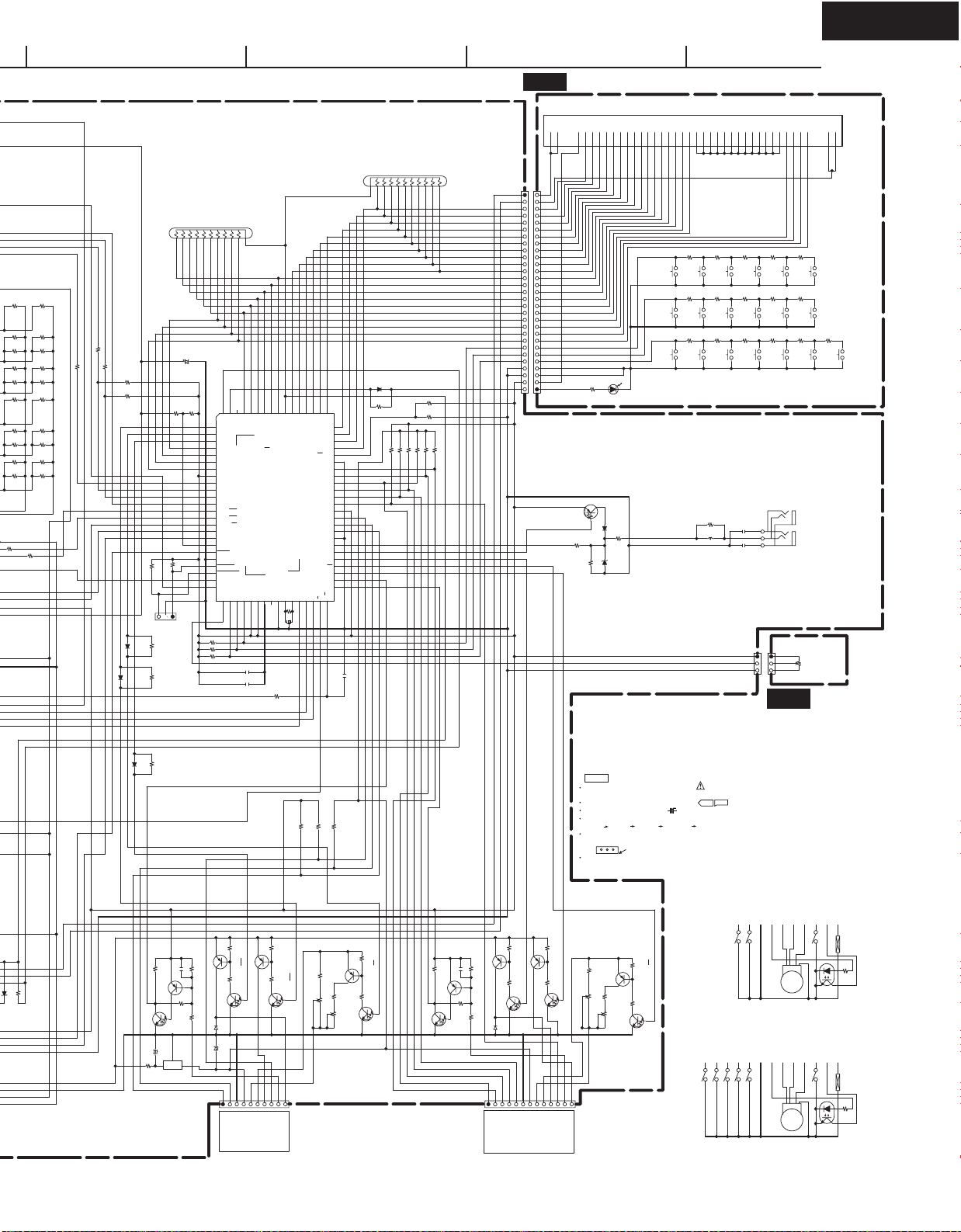
Page 8
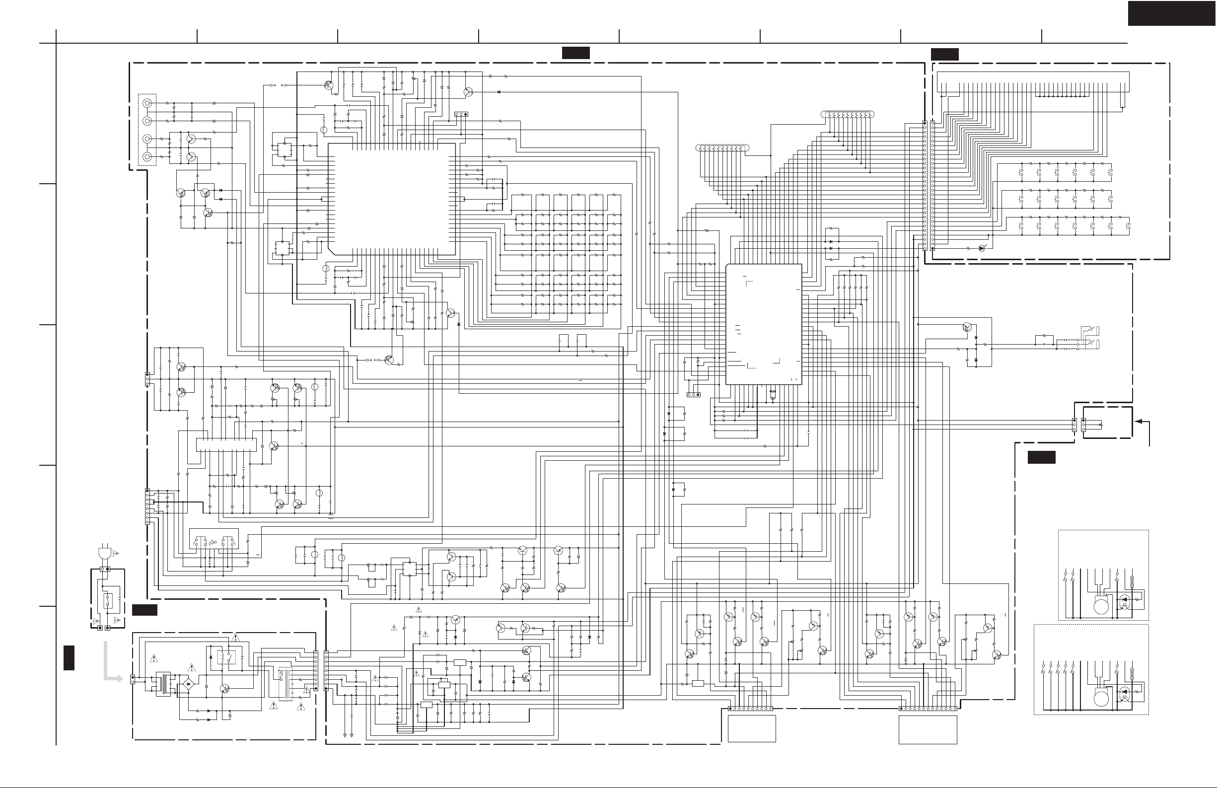
TA-RW255
SCHEMATIC
DIAGRAM
<MDD> ONLY
A
1
2
3
4
5
BCDEFGH
BIAS_CTRL
BIAS_NORM
BIAS_H
P-OFF
RESET
DECK_B_70/120
DECK_A_70/120
LINE_MUTE
PB_X1/X2
LINE_MUTE
SOL_A_ON/OFF
CAP_A_X1/X2
CAP_A_ON/OFF
REC/PB
CAP_B_X1/X2
SOL_B
CAP_B
+5V
+12VM
REC_MUTE
+12VA
-17V
SIG_L
SIG_RCH
DECK_B/A
1G
4G
P15
P10P9P8P7P6P5P4P3P2
P1
1G2G3G
4G
P15
P14
P13
P12
P11
P10
P9
P8
P7
P6
P5
P4
P3
P2
P1
1G
2G
3G
4G
KEY0
KEY1
KEY2
HIGH SW
PACK SW
REC INH FWD
FM
FQ
F/Q
GH
GL
GP
N.NORMN.HIGHN.MTLH.NORMH.HIGHH.MTL
A:H/B:L
HIGH SPEED
NORM SPEED
LCHRCH
A_PB_LCH B_PB_LCH
B_PB_RCH
A_PB_RCH
NORM SPEED
HIGH SPEED
TEST_MODE
DECK A
REC INH REV
METAL SW
MOTOR +
MOTOR B
MOTOR A
ROT PH DIODE
MOTER -
FT
PACK SW
HIGH SW
MOTER -
ROT PH DIODE
MOTOR A
MOTOR B
MOTOR +
PLAY SW
ROT PH OUT A
SOLENOID
ROT PH OUT B
SOLENOID
PLAY SW
DECK B
NAAF-8555
F-PLAY R-PLAY DOLBY_NRREWFFSTOP
DECK_B
STOP B-FF B-REW B_F-PLAY B_R-PLAY REV_MODE
STBY
ON/OFF
REC_PAUSE
AUTO_SPACE
NORM_DUBB
HIGH_DUBB
COUNTER
RESET
COUNTER
A/B
DECK_A
NADIS-8556
NAETC-8558
INPUT VR
NAPS-8557
BA-+
MOTOR
DECK B
BA-+
MOTOR
SOL
SOL
DECK A
Alternative use C904 or C916.
OTP ONLY
OTP ONLY
7
+5V SENSOR
6
MOTOR A5MOTOR B
8
MOTOR- COM
9
HIGH SW
10
PACK SW
11
REC INH FWD
12
REC INH REV
13
METAL SW
4
MOTOR+
3
PLAY SW
2
ROT PHT OUT
1
SOLENOID
7
+5V SENSOR
6
MOTOR A5MOTOR B
4
MOTOR+
3
PLAY SW
2
ROT PHT OUT
1
SOLENOID
8
MOTOR- COM
9
HIGH SW
10
PACK SW
R405
4.7
R406
4.7
Q407
2SC1959
C105
681
C106
681
R103
100K
R104
100K
C109
333
R109
100K
R111
3.3K
C113
681
R113
3.9K
C111
153
R115
10K
R108
3.9K
C110
333
R110
100K
C112
153
R112
3.3K
C114
681
R116
10K
C123
470/16
+
C126
101
R823
3.9K
R825
3.9K
R826
18K
C804
223
R910
5.6K
R911
5.6K
D601
1SS352
D602
1SS352
R114
3.9K
R224
10K
R220
100K
R214
560
C216
222
C218
104
C220
104
C210
222
R212
22K
C214
104
R229
12K
R211
22K
C211
222
R213
560
C213
104
C219
104
C217
104
C215
222
C209
222
R227
12K
R250
100K
R251
56K
R252
NC
R253
56K
R254
NC
R255
56K
R256
82K
R257
NC
R258
100K
R259
NC
R260
180K
R261
68K
R262
1M
R263
100K
R264
100K
R265
120K
R266
220K
R267
220K
R268
120K
R269
NC
R270
220K
R271
47K
R272
1M
R273
47K
R274
NC
R275
150K
R276
120K
R277
NC
R278
330K
R279
330K
R280
220K
R281
33K
R282
330K
R283
47K
R284
150K
R285
33K
R286
100K
R287
1M
R288
82K
R289
NC
R290
82K
R291
33K
R292
330K
R293
33K
R295
82K
R296
120K
R297
NC
R298
180K
R299
NC
R294
220K
R300
82K
R301
47K
R302
47K
R303
33K
R304
NC
R305
100K
R306
150K
R307
NC
R308
220K
R309
NC
R727
470
C712
104
R751
100K
R416
5.6K
Q809 2SB1068
R822
47K
R824
47K
R829
1M
R122
100(1/2W)
R121
4.7K
Q604
KRA107S
R817
2KB
2
3 1
R820
100K
Q812
2SA933S
R807
47K
R808
3.9K
R809
47K
Q805 2SB1068
R810
3.9K
R812
18K
C803
223
R107
3.9K
R408
39K
C404 472
Q406
2SC1959
R415
47K
R410
1K
R414
2.2K
R413
10K
R407
39K
C403 472
Q401
2SB1068
Q403
2SC1959
C206
1/50
+
C205
1/50
+
R231
18K
R241
3.3K
R242
3.3K
R243
6.8K
R244
6.8K
R215
4.7K
R217
3.3K
C223
1/50
+
R216
4.7K
R218
3.3K
C224
1/50
+
C228
2.2/50
+
C227
2.2/50
+
R417
100(1/2W)
Q603
KRA107S
R409
10(1/2W)
R411
820
C406
183
R831
1M
C241
1/50
+
C602
470/16
+
C601
1/50
+
C208
10/16
+
R201
22K
R202
22K
R203
68K
L203
NCH2137
2 1
R228
12K
C229
4.7/50
+
R222
10K
R221
10K
C230
4.7/50
+
R230
12K
C232
4.7/50
+
C231
4.7/50
+
D201
1SS352
D202
1SS352
Q203
RN1411
Q408 uPC1330HA
123
4
CNT
5
GND6VCC
789
L201
NMC6079
3
2
176
5
4
8
L202
NMC6079
6
5
4
8
3
2
1
7
C102
221
R101
100K
C101
221
R102
100K
C104
471
C103
471
C707
104
C918
2.2/50
+
R914
2.2K
R915
2.2K
R909
2.7K
C932
104
R725
22K
Q706
2SD655
R724
22K
Q705
2SD655
R728
0
C911
273
C212
222
C238
331
C237
331
C407
123/100V
C402
101
L403
NLO-2059
3
2
1
8
6
5
4
7
R404
100KB
123
R403
100KB
123
R119
50KB
2
13
R117
50KB
2
13
R118
50KB
2
31
R120
50KB
2
31
R772
180(1/2W)
Q101 BA3416BL
13579
111315
17
1816141210
864
2
R805
100K
R802
2KB
2
3 1
Q801
2SB1068
Q804
2SA933S
Q813
2SB1068
R733
2.7K
R734
2.7K
R735
2.7K
R742
4.7K
R738
4.7K
P5021
2
3
C722
104Z
C721
104Z
Q702
KRA107S
D701
1SS352
R748
470
R747
220K
R781100KX10
11
10
987654321
R783
0
R745
4.7K
D704
1SS352
R830
10K
Q815
2SA1037AK
R828
10K
Q807
2SA1037AK
R786
0
L701
BK1608LM182-T
R237
56K
R238
47K
R240
100K
R239
100K
R245
10K
C236
104
C235
104
P205
321
C125
101
C401
101
C409
223
D702
UDZS5.6B
D703
UDZS5.6B
R782 100KX10
123456789
10
11
R791
0
D708
1SS352
D707
1SS352
R792
0
R793
0
P705
1
2
3
D709
1SS352
D801
1N4003
2
1
D802
1N4003
2 1
C405 223
R903
3.9K
C914
104
R912
2.2K
R913
2.2K
Q903
78M05
1
I
2
G
3
O
Q901
78M12
1
I
2
G
3
O
R923
10(1/2W)
D907
UDZS18C
D904 1N4003
2 1
D9031N4003
2 1
D902 1N4003
2 1
D9011N4003
2 1
D913
1N4003
2 1
C915
1/50
+
Q904
2SA933S
C910
2200/16
+
R731
4.7K
R732
4.7K
R744
4.7K
R743
4.7K
R741
4.7K
R739
4.7K
R740
4.7K
R797
10K
R798
0
P701A
1
2
3
4
5
6
7
8
9
10
11
12
13
14
15
16
17
18
19
20
21
22
23
24
25
26
27
28
29
P102A
8
7
6
5
4
3
2
1
P101A
1
2
3
R746
47K
P801A
123456789
10
L401
4.7mH
NCH2133
2 1
C413
681
C415
680
C414
681
C416
680
Q902
7812
1
I
4
2
G
5
3
O
D911
1SS352
D905
1N4003
1 2
R924
680
R925
680
R926
680
D923
1SS352
D924
1SS352
C923
22/50
R737
4.7K
Q703
78L05
1I3
O
2
G
P702A
1
2
3
R902
1(1/2W)
C912
10/50
+
C913
47/50
+
D906
1N4003
21
Q906
KRA107S
R726
470
R723
22K
Q201
HA12169FB
61
VREF2
62
NRIN2
63
IAOUT2
64
BIAS
65
RPI2
66
VRI32
67
VRI22
68
CONT2
69
VRI12
70
GND22
71
GND11
72
VRI11
73
CONT1
74
VRI21
75
VRI31
76
RPI1
77
REF1
78
IAOUT1
79
NRIN1
80
VREF1
1
BIASTRAP12PBOUT13SS114SS215CCR16HLS17LLS18RECOUT19LMIN1
10
LMDET111LMOUT112EQIN113EQCONT114IREF15EQOUT116NN17NH18NM19HN20HH
21
HM
22
GP
23
GL
24
GH
25
F/Q
26
FQ
27
FM
28
BIASCONT1
29
DACOUT1
30
VCC
31
VCC
32
DACOUT2
33
BIASCONT2
34
GND
35
BIASADJN
36
BIASADJM
37
BIASADJH
38
INJ
39
CLK
40
DATA
41
STB
42
RESET
43
MPX
44
C/B
45
NRONOFF
46
EQOUT2
47
DGND
48
EQCONT2
49
EQIN2
50
LMOUT2
51
LMDET2
52
LMIN2
53
RECOUT2
54
LLS2
55
HLS2
56
CCR2
57
SS2258SS12
59
PBOUT2
60
BIASTRAP2
R236
47K
R235
3.3K
R813
47K
R827
47K
P802A
12345678910111213
R801
6.8K
R816
6.8K
R803
1KB
2
3 1
R818
1KB
2
3 1
R821
10K
R806
10K
R105
33
R106
33
C108
470/6.3
+
R226
20KB
1
2
3
R311
10K
R312
10K
R123
560
R223
10K
R225
20KB
2
1 3
R219
100K
C128
223
Q204
RN1411
L204
NCH2137
1 2
C764
223
C763
223
R753
3.3K
R754
3.3K
R601
2.2K
R232
0
R233
0
R234
0
C127
104
R310
10K
C233
0.1/50
+
C919
100/25
+
Q701
MPD78042FGF
1
CAP_A
2
CAP_A_X2/X1
3
SOL_A
4
1G
5
2G
6
3G
7
4G
8
VDD
9
DOL_CLK
10
DOL_DATA
11
DOL_STB
12
DOL_RST
13
A_70/120
14
B_70/120
15
PB_X1/X2
16
LINE_MUTE
17
RESET
18
REC MUTE
19
P-OFF
20
AVSS
21
FT_MODE
22
TEST_MODE
23
SIG_LCH
24
SIG_RCH
25
VOL
26
KEY227KEY1
28
KEY029AVDD
30
AVREF
31
XT1/GND32XT2/NC
33
VSS34X135X2
36
BIAS_CONT37N.BIAS38H.BIAS39R/P
40
B/A
41
R.SEN_B
42
R.SEN_A
43
CAP_B
44
CAP_B_X1/X2
45
SOL_B
46
RI_OUT
47
RI_IN
48
IC(VPP)GND
49
A_PACK_SW
50
A_HIGH_SW
51
A_PLY_SW
52
VDD
53
B_PLY_SW
54
B_HIGH_SW
55
B_PACK_SW
56
B_F.REC_INH
57
B_MTL_SW
58
B_R.REC_INH
59
NC
60
SRCH_OFF/ON
61
P16
62
P15
63
P14
64
P13
65
P1266P1167P10
68P969P870P771
VDISP
72P673P574P475P376P277P178
RELAY
79
S_LED
80
FL
R771
2.2K
R721
4.7K
R722
4.7K
R749
1K
C725
22/50
R314
56
R313
56
R204
68K
J2A
1
J2B
1
J1A
1
J1B
1
E002 E001
C903
104
C907
104
C934
223
R819
1K
R804
1K
Q102
KRC107S
Q103
KRC107S
Q104
KRC107S
Q905
KRC107S
Q404
KRC107S
Q605
KRC107S
Q811
KRC107S
Q806
KRC107S
Q808
KRC107S
Q105
KRC107S
Q402
KRC107S
Q405
KRC107S
Q107
KRC107S
Q108
KRC107S
Q803
KRC107S
Q802
KRC107S
Q810
KRC107S
Q814
KRC107S
Q816
KRC107S
Q206
KRC107S
Q205
KRC107S
C107
470/6.3
+
C115
10/50
+
C116
10/50
+
C122
10/50
+
C121
22/50
+
C202
10/50
+
C201
10/50
+
C203
10/50
+
C204
10/50
+
C207
10/50
+
C221
100/25
+
C222
100/25
+
C226
10/50
+
C225
10/50
+
C239
10/50
+
C240
10/50
+
C408
10/50
+
C410
22/50
+
C411
220/25
+
C761
10/50
+
C762
10/50
+
C905
10/50
+
C906
100/25
+
C908
220/25
+
C909
10/50
+
X701
CSTLS5M00
R736
NC
R752
3.3K
C765
223
P201
2
1
3
5
4
6
S704
S705
S708
S710
S711
S712
S713
S714
S715
S716
S717
S719
S718
R702
470
R703
820
R7041KR705
1.8K
R706
390
R707
470
R708
820
R7091KR710
1.8K
R711
390
R712
470
R713
820
R7141KR715
1.8K
S702S709
R701
390
S703
R716
3.9K
S720
S706
S701
R717
3.9K
D706
SLI-343URC-TE7
Q707 BJ246GK
1
F112F125P176P167P158P149P13
10
P1211P1112P1013P914P815P716P617P518P419P320P221P122NC23NC24NC25NC26NC27NC28NC29NC30NC31NC32NC33NC34NC351G362G373G384G41F2142F22
P701B
1
2
3
4
5
6
7
8
9
10
11
12
13
14
15
16
17
18
19
20
21
22
23
24
25
26
27
28
29
R761
20KB
2
1
3
P702B
3
2
1
JL902A
5
4
3
2
1
JL902B
1
2
3
4
5
T901
NPT-1523D
6
5
2 15
14
NC
13
12
NC
11
10
9
D910
UDZS5.6B
C723
104
C724
223
L101
NCH2137
1 2
C117
331
L402
4.7mH
NCH2133
2 1
P901
2
1
P901A
C118
331
Q106
KRC107S
L102
NCH2137
2
1
R206
1K
R205
1K
R207
6.8K
R208
6.8K
Q602
2SD655
Q601
2SD655
R315
100
R316
100
R209
2.2K
R210
2.2K
R125
470
R126
470
R127
470
R128
470
C904
13000/25
+
THE COMPONENTS IDENTIFIED BY MARK ARE CRITICAL FOR SAFETY.
REPLACE ONLY WITH PART NUMBER SPECIFIED.
VOLTAGE (MEASURED WITH VOLTMETER) IS DC VOLTAGE. (NO INPUT SIGNAL)
ELECTROLYTIC CAPACITORS ARE IN uF/WV.
ALL CAPACITORS ARE IN pF/50WV UNLESS OTHERWISE NOTED.
EX) 030 3pF 330 33pF 331 330pF 333 0.033uF
ALL RESISTORS ARE IN OHMS 1/4WATTS UNLESS OTHERWISE NOTED.
THE THICK LINES ON PC BOARD ARE THE PRINTING SIDE OF THE PARTS.
EX) PRINTING SIDE
CIRCUIT IS SUBJECT TO CHANGE FOR IMPROVEMENT.
NOTE
( )
NAAF-8555
U01 MAIN PC BOARD NAAF-8555
U02
DISPLAY CIRCUIT PC BOARD
NADIS-8556
U04
INPUT VOLUME
PC BOARD
NAETC-8558
U03
POWER SUPPLY PC BOARD
NC
NC
NC
NC
NC
NC
DECK A
DECK B
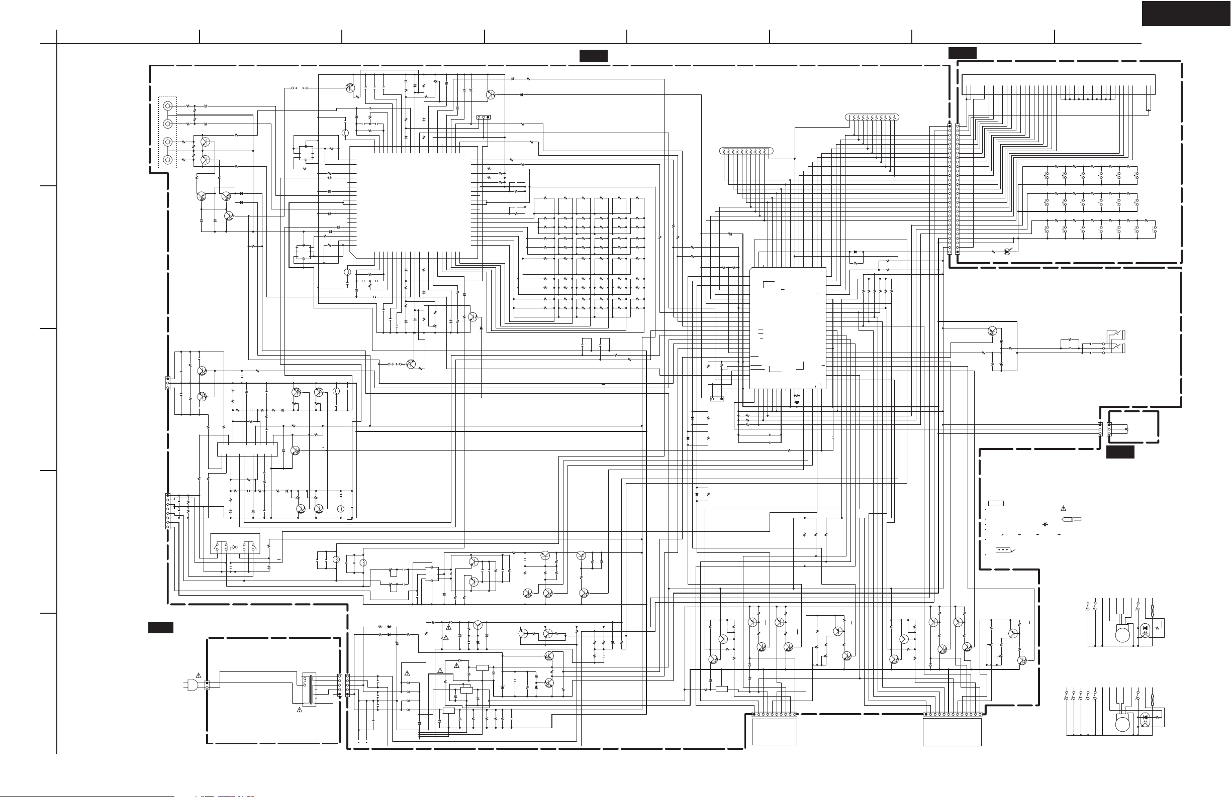
Page 9
BIAS_CTRL
BIAS_NORM
BIAS_H
P-OFF
RESET
DECK_B_70/120
DECK_A_70/120
LINE_MUTE
PB_X1/X2
LINE_MUTE
REC/PB
+5V
+12VM
+12VA
GND_T
-17V
SIG_L
DECK_B/A
N.NORMN.HIGHN.MTLH.NORMH.HIGHH.MTL
A:H/B:L
LCHRCH
A_PB_LCH B_PB_LCH
B_PB_RCHA_PB_RCH
PP,PA MODEL
PP,PA MODEL
NPT-1523P
NPT-1524P
R405
4.7
R406
4.7
Q407
2SC1959
C105
681
C106
681
R103
100K
R104
100K
C109
333
R109
100K
R111
3.3K
C113
681
R113
3.9K
C111
153
R115
10K
R108
3.9K
C110
333
R110
100K
C112
153
R112
3.3K
C114
681
R116
10K
C123
470/16
+
C118
331
R910
5.6K
R911
5.6K
D601
1SS352
D602
1SS352
R114
3.9K
R224
10K
R220
100K
R214
560
C216
222
C218
104
C220
104
C210
222
R212
22K
C214
104
R229
12K
R211
22K
C211
222
R213
560
C213
104
C219
104
C217
104
C215
222
C209
222
R227
12K
R250
100K
R251
56K
R252
NC
R253
56K
R254
NC
R255
56K
R256
82K
R257
NC
R258
100K
R259
NC
R260
180K
R261
68K
R262
1M
R263
100K
R264
100K
R265
120K
R266
220K
R267
220K
R268
120K
R269
NC
R270
220K
R271
47K
R272
1M
R273
47K
R274
NC
R275
150K
R276
120K
R277
NC
R278
330K
R279
330K
R280
220K
R281
33K
R282
330K
R283
47K
R284
150K
R285
33K
R286
100K
R287
1M
R288
82K
R289
NC
R290
82K
R291
33K
R292
330K
R293
33K
R295
82K
R296
120K
R297
NC
R298
180K
R299
NC
R294
220K
R300
82K
R301
47K
R302
47K
R303
33K
R304
NC
R305
100K
R306
150K
R307
NC
R308
220K
R309
NC
R727
470
C712
104
R751
100K
R416
5.6K
R122
100(1/2W)
R121
4.7K
Q604
KRA107S
R107
3.9K
R408
39K
C404 472
Q406
2SC1959
R415
47K
R410
1K
R414
2.2K
R413
10K
R407
39K
C403 472
Q401
2SB1068
Q403
2SC1959
C206
1/50
+
C205
1/50
+
R231
18K
R241
3.3K
R242
3.3K
R243
6.8K
R244
6.8K
R215
4.7K
R217
3.3K
C223
1/50
+
R216
4.7K
R218
3.3K
C224
1/50
+
C228
2.2/50
+
C227
2.2/50
+
R417
100(1/2W)
Q603
KRA107S
R409
10(1/2W)
R411
820
C406
183
C241
1/50
+
C602
470/16
+
C601
1/50
+
C208
10/16
+
L203
NCH2137
2 1
R228
12K
C229
4.7/50
+
R222
10K
R221
10K
C230
4.7/50
+
R230
12K
C232
4.7/50
+
C231
4.7/50
+
D201
1SS352
D202
1SS352
Q203
RN1411
Q408 uPC1330HA
123
4
CNT
5
GND
6
VCC
789
L201
NMC6079
3
2
176
5
4
8
L202
NMC6079
6
5
483
2
1
7
C102
221
R101
100K
C101
221
R102
100K
C104
471
C103
471
C707
104
C918
2.2/50
+
R914
2.2K
R915
2.2K
R908
470
R909
2.7K
C932
104
R725
22K
Q706
2SD655
R724
22K
Q705
2SD655
R728
0
C911
273
C212
222
C238
331
C237
331
C407
123/100V
C402
101
L403
NLO-2059
3
2
186
5
4
7
R404
100KB
123
R403
100KB
123
R119
50KB
2
13
R117
50KB
2
13
R118
50KB
2
31
R120
50KB
2
31
Q101 BA3416BL
13579
11
131517
1816141210
864
2
R237
56K
R238
47K
R240
100K
R239
100K
R245
10K
C236
104
C235
104
P205
321
C401
101
C409
223
D703
UDZS5.6B
C405 223
R903
3.9K
C914
104
R912
2.2K
R913
2.2K
Q903
78M05
1
I
2
G
3
O
Q901
78M12
1
I
2
G
3
O
R923
10(1/2W)
D907
UDZS18C
D908
1N4003
2 1
D904 1N4003
2 1
D9031N4003
2 1
D902 1N4003
2 1
D9011N4003
2 1
D913
1N40032 1
C915
1/50
+
Q904
2SA933S
C910
2200/16
+
P102A
8
7
6
5
4
3
2
1
P101A
1
2
3
L102
NCH2137
2 1
L401
4.7mH
NCH2133
2 1
C413
681
C415
680
C414
681
C416
680
L402
4.7mH
NCH2133
2 1
Q902
7812
1
I
4
2
G
5
3
O
D911
1SS352
D905
1N4003
1 2
R902
1(1/2W)
C912
10/50
+
C913
47/50
+
D906
1N4003
21
Q906
KRA107S
R726
470
R723
22K
Q201
HA12169FB
61
VREF2
62
NRIN2
63
IAOUT2
64
BIAS
65
RPI2
66
VRI32
67
VRI22
68
CONT2
69
VRI12
70
GND22
71
GND11
72
VRI11
73
CONT1
74
VRI21
75
VRI31
76
RPI1
77
REF1
78
IAOUT1
79
NRIN1
80
VREF1
1
BIASTRAP12PBOUT13SS114SS215CCR16HLS17LLS18RECOUT19LMIN1
10
LMDET111LMOUT112EQIN113EQCONT114IREF15EQOUT116NN17NH18NM19HN20HH
21
HM
22
GP
23
GL
24
GH
25
F/Q
26
FQ
27
FM
28
BIASCONT1
29
DACOUT1
30
VCC
31
VCC
32
DACOUT2
33
BIASCONT2
34
GND
35
BIASADJN
36
BIASADJM
37
BIASADJH
38
INJ
39
CLK
40
DATA
41
STB
42
RESET
43
MPX
44
C/B
45
NRONOFF
46
EQOUT2
47
DGND
48
EQCONT2
49
EQIN2
50
LMOUT2
51
LMDET2
52
LMIN2
53
RECOUT2
54
LLS2
55
HLS2
56
CCR2
57
SS2258SS12
59
PBOUT2
60
BIASTRAP2
R236
47K
R235
3.3K
R105
33
R106
33
C108
470/6.3
+
R226
20KB
1
2
3
R123
560
R223
10K
R225
20KB
2
1 3
R219
100K
C128
223
Q204
RN1411
L204
NCH2137
1 2
C764
223
C763
223
R753
3.3K
R754
3.3K
R601
2.2K
R232
0
R233
0
R234
0
C127
104
C233
0.1/50
+
C919
100/25
+
R314
56
R313
56
J2A
1
J2B
1
J1A
1
J1B
1
JL901B
1
2
3
4
5
6
7
8
9
E001
C903
104
C907
104
C934
223
Q102
KRC107S
Q103
KRC107S
Q104
KRC107S
Q106
KRC107S
Q905
KRC107S
Q404
KRC107S
Q605
KRC107S
Q105
KRC107S
Q402
KRC107S
Q405
KRC107S
Q107
KRC107S
Q108
KRC107S
Q206
KRC107S
Q205
KRC107S
C107
470/6.3
+
C115
10/50
+
C116
10/50
+
C122
10/50
+
C121
22/50
+
C203
10/50
+
C204
10/50
+
C207
10/50
+
C221
100/25
+
C222
100/25
+
C226
10/50
+
C225
10/50
+
C239
10/50
+
C240
10/50
+
C408
10/50
+
C410
22/50
+
C411
220/25
+
C905
10/50
+
C906
100/25
+
C908
220/25
+
C909
10/50
+
Q921
KRC107S
D922
1N4003
D931
1SS352
D932
1SS352
P901
2
1
RL901
3
1 4
2
D921
421
3
R921
470
R922
470
C922
470/16
+
T901
NPT-1523
6
5
2
15
14
NC
13
12
NC
11
10
9
T902
NPT-1524
4
3
2
1
9
8
NC
7
NC
6
5
C921
103M
JL901A
9
8
7
6
5
4
3
2
1
C931
22/50
+
J901B
1
S901
1 2
J901A
1
C933
103M
D910
UDZS5.6B
L101
NCH2137
1 2
C117
331
C125
221
C126
221
P902
2
1
P902A
R125
470
R126
470
R127
470
R128
470
R201
22K
R202
22K
R203
68K
R204
68K
P201
2
1
3
5
4
6
C202
10/50
+
C201
10/50
+
C243
181
R206
1K
R205
1K
R207
6.8K
R208
6.8K
R209
2.2K
R210
2.2K
Q602
2SD655
C244
181
Q601
2SD655
C247
332
C248
332
R315
100
R316
100
C904
13000/25
+
E002
R930
2.5A/125V
R931
2.5A/125V
EXCEPT
<MDD>
U01 MAIN PC BOARD NAAF-8555
NAPS-8557
U03
POWER SUPPLY
PC BOARD
U05
POWER SWITCH
PC BOARD NASW-8559
DECK B
DECK A
NC
NC
NC
NC
NC
NC
SCHEMATIC DIAGRAM
A
1
2
3
4
5
BCDEFGH
Page 10
P-OFF
RESET
SOL_A_ON/OFF
CAP_A_X1/X2
CAP_A_ON/OFF
CAP_B_X1/X2
SOL_B
CAP_B
REC_MUTE
SIG_L
SIG_RCH
1G
4G
P15
P10P9P8P7P6P5P4P3P2
P1
1G2G3G
4G
P15
P14
P13
P12
P11
P10
P9
P8
P7
P6
P5
P4
P3
P2
P1
1G
2G
3G
4G
KEY0
KEY1
KEY2
HIGH SW
PACK SW
REC INH FWD
FM
FQ
F/Q
GH
GL
GP
N.NORMN.HIGHN.MTLH.NORMH.HIGHH.MTL
HIGH SPEED
NORM SPEED
NORM SPEED
HIGH SPEED
TEST_MODE
DECK A
REC INH REV
METAL SW
MOTOR +
MOTOR B
MOTOR A
ROT PH DIODE
MOTER -
FT
PACK SW
HIGH SW
MOTER -
ROT PH DIODE
MOTOR A
MOTOR B
MOTOR +
PLAY SW
ROT PH OUT A
SOLENOID
ROT PH OUT B
SOLENOID
PLAY SW
DECK B
F-PLAY
R-PLAY
DOLBY_NR
REW
FF
STOP
DECK_B
STOP
B-FF
B-REW
B_F-PLAY
B_R-PLAY
REV_MODE
STBY
ON/OFF
REC_PAUSE
AUTO_SPACE
NORM_DUBB
HIGH_DUBB
COUNTER
RESET
COUNTER
A/B
DECK_A
NAETC-8558
INPUT VR
BA-+
MOTOR
DECK B
BA-+
MOTOR
SOL
SOL
DECK A
OTP ONLY
OTP ONLY1
NAAF-8555
7
+5V SENSOR
6
MOTOR A5MOTOR B
8
MOTOR- COM
9
HIGH SW
10
PACK SW
11
REC INH FWD
12
REC INH REV
13
METAL SW
4
MOTOR+
3
PLAY SW
2
ROT PHT OUT
1
SOLENOID
7
+5V SENSOR
6
MOTOR A5MOTOR B
4
MOTOR+
3
PLAY SW
2
ROT PHT OUT
1
SOLENOID
8
MOTOR- COM
9
HIGH SW
10
PACK SW
R823
3.9K
R825
3.9K
R826
18K
C804
223
R250
100K
R251
56K
R252
NC
R253
56K
R254
NC
R255
56K
R256
82K
R257
NC
R258
100K
R259
NC
100K
Q809 2SB1068
R822
47K
R824
47K
R829
1M
R817
2KB
2
3 1
R820
100K
Q812
2SA933S
R807
47K
R808
3.9K
R809
47K
Q805 2SB1068
R810
3.9K
R812
18K
C803
223
R831
1M
R772
180(1/2W)
R805
100K
R802
2KB
2
3 1
Q801
2SB1068
Q804
2SA933S
Q813 2SB1068
R733
2.7K
R734
2.7K
R735
2.7K
R742
4.7K
R738
4.7K
P5021
2
3
C722
104Z
C721
104Z
Q702
KRA107S
D701
1SS352
R748
470
R747
220K
R781100KX10
11
10
987654321
R783
0
R745
4.7K
D704
1SS352
D705
1SS352
R784
0
R830
10K
Q815
2SA1037AK
R828
10K
Q807
2SA1037AK
R786
0
L701
BK1608LM182-T
D702
UDZS5.6B
R782 100KX10
123456789
10
11
R791
0
D708
1SS352
D707
1SS352
R792
0
R793
0
P705
1
2
3
D709
1SS352
D801
1N4003
2 1
D802
1N4003
2 1
R731
4.7K
R732
4.7K
R744
4.7K
R743
4.7K
R741
4.7K
R739
4.7K
R740
4.7K
R797
10K
R798
0
P701A
1
2
3
4
5
6
7
8
9
10
11
12
13
14
15
16
17
18
19
20
21
22
23
24
25
26
27
28
29
R746
47K
P801A
123456789
10
R737
4.7K
Q703
78L05
1I3
O
2
G
P702A
1
2
3
R813
47K
R827
47K
P802A
12345678910111213
R803
1KB
2
3 1
R818
1KB
2
3 1
R821
10K
R806
10K
R311
10K
R312
10K
R754
3.3K
R310
10K
Q701
MPD78042FGF
1
CAP_A
2
CAP_A_X2/X1
3
SOL_A
4
1G
5
2G
6
3G
7
4G
8
VDD
9
DOL_CLK
10
DOL_DATA
11
DOL_STB
12
DOL_RST
13
A_70/120
14
B_70/120
15
PB_X1/X2
16
LINE_MUTE
17
RESET
18
REC MUTE
19
P-OFF
20
AVSS
21
FT_MODE
22
TEST_MODE
23
SIG_LCH
24
SIG_RCH
25
VOL26KEY227KEY128KEY029AVDD30AVREF31XT1/GND32XT2/NC33VSS34X135X236BIAS_CONT37N.BIAS38H.BIAS39R/P40B/A
41
R.SEN_B 41
42
R.SEN_A
43
CAP_B
44
CAP_B_X1/X2
45
SOL_B
46
RI_OUT
47
RI_IN
48
IC(VPP)GND
49
A_PACK_SW
50
A_HIGH_SW
51
A_PLY_SW
52
VDD
53
B_PLY_SW
54
B_HIGH_SW
55
B_PACK_SW
56
B_F.REC_INH
57
B_MTL_SW
58
B_R.REC_INH
59
NC
60
SRCH_OFF/ON
61
P16
62
P15
63
P14
64
P13
65
P1266P1167P10
68P969P870P771
VDISP
72P673P574P475P376P277P178
RELAY
79
S_LED
80
FL
R771
2.2K
R721
4.7K
R722
4.7K
R749
1K
C725
22/50
R819
1K
R804
1K
Q811
KRC107S
Q806
KRC107S
Q808
KRC107S
Q803
KRC107S
Q802
KRC107S
Q810
KRC107S
Q814
KRC107S
Q816
KRC107S
C761
10/50
+
C762
10/50
+
X701
CSTLS5M00
R736
NC
R752
3.3K
C765
223
S704
S705
S708
S710
S711
S712
S713
S714
S715
S716
S717
S719
S718
R702
470
R703
820
R704
1K
R705
1.8K
R706
390
R707
470
R708
820
R709
1K
R710
1.8K
R711
390
R712
470
R713
820
R714
1K
R715
1.8K
S702S709
R701
390
S703
R716
3.9K
S720
S706
S701
R717
3.9K
D706
SLI-343URC-TE7
Q707 BJ246GK
1
F112F125P176P167P158P149P13
10
P1211P1112P1013P914P815P716P617P518P419P320P221P122NC23NC24NC25NC26NC27NC28NC29NC30NC31NC32NC33NC34NC351G362G373G384G41F2142F22
P701B
1
2
3
4
5
6
7
8
9
10
11
12
13
14
15
16
17
18
19
20
21
22
23
24
25
26
27
28
29
R761
20KB
2
1
3
P702B
3
2
1
C723
104
C724
223
R816
5.6K
R801
5.6K
NC
NC
U02 DISPLAY CIRCUIT PC BOARD
NADIS-8556
U04
INPUT VOLUME
PC BOARD
NAETC-8558
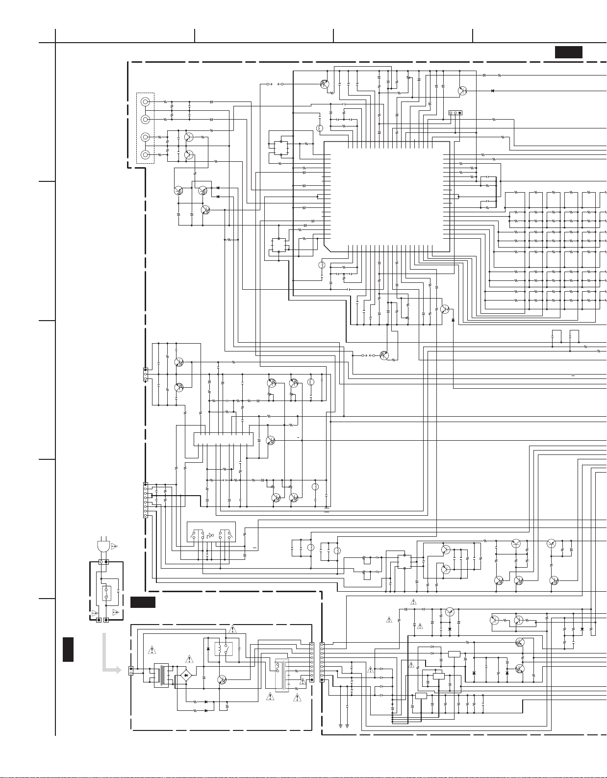
TA-RW255
Page 11
BIAS_CTRL
BIAS_NORM
BIAS_H
P-OFF
RESET
DECK_B_70/120
DECK_A_70/120
LINE_MUTE
PB_X1/X2
LINE_MUTE
SOL_A_ON/OFF
CAP_A_X1/X2
CAP_A_ON/OFF
REC/PB
CAP_B_X1/X2
SOL_B
CAP_B
+5V
+12VM
REC_MUTE
+12VA
GND_T
-17V
SIG_L
SIG_RCH
DECK_B/A
1G
4G
P15
P10P9P8P7P6P5P4P3P2
P1
1G2G3G
4G
P15
P14
P13
P12
P11
P10
P9
P8
P7
P6
P5
P4
P3
P2
P1
1G
2G
3G
4G
KEY0
KEY1
KEY2
HIGH SW
PACK SW
REC INH FWD
FM
FQ
F/Q
GH
GL
GP
N.NORMN.HIGHN.MTLH.NORMH.HIGHH.MTL
A:H/B:L
HIGH SPEED
NORM SPEED
LCHRCH
A_PB_LCH B_PB_LCH
B_PB_RCHA_PB_RCH
NORM SPEED
HIGH SPEED
TEST_MODE
DECK A
REC INH REV
METAL SW
MOTOR +
MOTOR B
MOTOR A
ROT PH DIODE
MOTER -
FT
PACK SW
HIGH SW
MOTER -
ROT PH DIODE
MOTOR A
MOTOR B
MOTOR +
PLAY SW
ROT PH OUT A
SOLENOID
ROT PH OUT B
SOLENOID
PLAY SW
DECK B
F-PLAY
R-PLAY
DOLBY_NR
REW
FF
STOP
DECK_B
STOP
B-FF
B-REW
B_F-PLAY
B_R-PLAY
REV_MODE
STBY
ON/OFF
REC_PAUSE
AUTO_SPACE
NORM_DUBB
HIGH_DUBB
COUNTER
RESET
COUNTER
A/B
DECK_A
NAETC-8558
INPUT VR
BA-+
MOTOR
DECK B
BA-+
MOTOR
SOL
SOL
DECK A
OTP ONLY
OTP ONLY1
NAAF-8555
PP,PA MODEL
PP,PA MODEL
NPT-1523P
NPT-1524P
7
+5V SENSOR
6
MOTOR A5MOTOR B
8
MOTOR- COM
9
HIGH SW
10
PACK SW
11
REC INH FWD
12
REC INH REV
13
METAL SW
4
MOTOR+
3
PLAY SW
2
ROT PHT OUT
1
SOLENOID
7
+5V SENSOR
6
MOTOR A5MOTOR B
4
MOTOR+
3
PLAY SW
2
ROT PHT OUT
1
SOLENOID
8
MOTOR- COM
9
HIGH SW
10
PACK SW
R405
4.7
R406
4.7
Q407
2SC1959
C105
681
C106
681
R103
100K
R104
100K
C109
333
R109
100K
R111
3.3K
C113
681
R113
3.9K
C111
153
R115
10K
R108
3.9K
C110
333
R110
100K
C112
153
R112
3.3K
C114
681
R116
10K
C123
470/16
+
C118
331
R823
3.9K
R825
3.9K
R826
18K
C804
223
R910
5.6K
R911
5.6K
D601
1SS352
D602
1SS352
R114
3.9K
R224
10K
R220
100K
R214
560
C216
222
C218
104
C220
104
C210
222
R212
22K
C214
104
R229
12K
R211
22K
C211
222
R213
560
C213
104
C219
104
C217
104
C215
222
C209
222
R227
12K
R250
100K
R251
56K
R252
NC
R253
56K
R254
NC
R255
56K
R256
82K
R257
NC
R258
100K
R259
NC
R260
180K
R261
68K
R262
1M
R263
100K
R264
100K
R265
120K
R266
220K
R267
220K
R268
120K
R269
NC
R270
220K
R271
47K
R272
1M
R273
47K
R274
NC
R275
150K
R276
120K
R277
NC
R278
330K
R279
330K
R280
220K
R281
33K
R282
330K
R283
47K
R284
150K
R285
33K
R286
100K
R287
1M
R288
82K
R289
NC
R290
82K
R291
33K
R292
330K
R293
33K
R295
82K
R296
120K
R297
NC
R298
180K
R299
NC
R294
220K
R300
82K
R301
47K
R302
47K
R303
33K
R304
NC
R305
100K
R306
150K
R307
NC
R308
220K
R309
NC
R727
470
C712
104
R751
100K
R416
5.6K
Q809 2SB1068
R822
47K
R824
47K
R829
1M
R122
100(1/2W)
R121
4.7K
Q604
KRA107S
R817
2KB
2
3 1
R820
100K
Q812
2SA933S
R807
47K
R808
3.9K
R809
47K
Q805 2SB1068
R810
3.9K
R812
18K
C803
223
R107
3.9K
R408
39K
C404 472
Q406
2SC1959
R415
47K
R410
1K
R414
2.2K
R413
10K
R407
39K
C403 472
Q401
2SB1068
Q403
2SC1959
C206
1/50
+
C205
1/50
+
R231
18K
R241
3.3K
R242
3.3K
R243
6.8K
R244
6.8K
R215
4.7K
R217
3.3K
C223
1/50
+
R216
4.7K
R218
3.3K
C224
1/50
+
C228
2.2/50
+
C227
2.2/50
+
R417
100(1/2W)
Q603
KRA107S
R409
10(1/2W)
R411
820
C406
183
R831
1M
C241
1/50
+
C602
470/16
+
C601
1/50
+
C208
10/16
+
L203
NCH2137
2 1
R228
12K
C229
4.7/50
+
R222
10K
R221
10K
C230
4.7/50
+
R230
12K
C232
4.7/50
+
C231
4.7/50
+
D201
1SS352
D202
1SS352
Q203
RN1411
Q408 uPC1330HA
123
4
CNT
5
GND
6
VCC
789
L201
NMC6079
3
2
176
5
4
8
L202
NMC6079
6
5
483
2
1
7
C102
221
R101
100K
C101
221
R102
100K
C104
471
C103
471
C707
104
C918
2.2/50
+
R914
2.2K
R915
2.2K
R908
470
R909
2.7K
C932
104
R725
22K
Q706
2SD655
R724
22K
Q705
2SD655
R728
0
C911
273
C212
222
C238
331
C237
331
C407
123/100V
C402
101
L403
NLO-2059
3
2
186
5
4
7
R404
100KB
123
R403
100KB
123
R119
50KB
2
13
R117
50KB
2
13
R118
50KB
2
31
R120
50KB
2
31
R772
180(1/2W)
Q101 BA3416BL
13579
11
131517
1816141210
864
2
R805
100K
R802
2KB
2
3 1
Q801
2SB1068
Q804
2SA933S
Q813 2SB1068
R733
2.7K
R734
2.7K
R735
2.7K
R742
4.7K
R738
4.7K
P5021
2
3
C722
104Z
C721
104Z
Q702
KRA107S
D701
1SS352
R748
470
R747
220K
R781100KX10
11
10
987654321
R783
0
R745
4.7K
D704
1SS352
D705
1SS352
R784
0
R830
10K
Q815
2SA1037AK
R828
10K
Q807
2SA1037AK
R786
0
L701
BK1608LM182-T
R237
56K
R238
47K
R240
100K
R239
100K
R245
10K
C236
104
C235
104
P205
321
C401
101
C409
223
D702
UDZS5.6B
D703
UDZS5.6B
R782 100KX10
123456789
10
11
R791
0
D708
1SS352
D707
1SS352
R792
0
R793
0
P705
1
2
3
D709
1SS352
D801
1N4003
2 1
D802
1N4003
2 1
C405 223
R903
3.9K
C914
104
R912
2.2K
R913
2.2K
Q903
78M05
1
I
2
G
3
O
Q901
78M12
1
I
2
G
3
O
R923
10(1/2W)
D907
UDZS18C
D908
1N4003
2 1
D904 1N4003
2 1
D9031N4003
2 1
D902 1N4003
2 1
D9011N4003
2 1
D913
1N40032 1
C915
1/50
+
Q904
2SA933S
C910
2200/16
+
R731
4.7K
R732
4.7K
R744
4.7K
R743
4.7K
R741
4.7K
R739
4.7K
R740
4.7K
R797
10K
R798
0
P701A
1
2
3
4
5
6
7
8
9
10
11
12
13
14
15
16
17
18
19
20
21
22
23
24
25
26
27
28
29
P102A
8
7
6
5
4
3
2
1
P101A
1
2
3
R746
47K
P801A
123456789
10
L102
NCH2137
2 1
L401
4.7mH
NCH2133
2 1
C413
681
C415
680
C414
681
C416
680
L402
4.7mH
NCH2133
2 1
Q902
7812
1
I
4
2
G
5
3
O
D911
1SS352
D905
1N4003
1 2
R737
4.7K
Q703
78L05
1I3
O
2
G
P702A
1
2
3
R902
1(1/2W)
C912
10/50
+
C913
47/50
+
D906
1N4003
21
Q906
KRA107S
R726
470
R723
22K
Q201
HA12169FB
61
VREF2
62
NRIN2
63
IAOUT2
64
BIAS
65
RPI2
66
VRI32
67
VRI22
68
CONT2
69
VRI12
70
GND22
71
GND11
72
VRI11
73
CONT1
74
VRI21
75
VRI31
76
RPI1
77
REF1
78
IAOUT1
79
NRIN1
80
VREF1
1
BIASTRAP12PBOUT13SS114SS215CCR16HLS17LLS18RECOUT19LMIN1
10
LMDET111LMOUT112EQIN113EQCONT114IREF15EQOUT116NN17NH18NM19HN20HH
21
HM
22
GP
23
GL
24
GH
25
F/Q
26
FQ
27
FM
28
BIASCONT1
29
DACOUT1
30
VCC
31
VCC
32
DACOUT2
33
BIASCONT2
34
GND
35
BIASADJN
36
BIASADJM
37
BIASADJH
38
INJ
39
CLK
40
DATA
41
STB
42
RESET
43
MPX
44
C/B
45
NRONOFF
46
EQOUT2
47
DGND
48
EQCONT2
49
EQIN2
50
LMOUT2
51
LMDET2
52
LMIN2
53
RECOUT2
54
LLS2
55
HLS2
56
CCR2
57
SS2258SS12
59
PBOUT2
60
BIASTRAP2
R236
47K
R235
3.3K
R813
47K
R827
47K
P802A
12345678910111213
R803
1KB
2
3 1
R818
1KB
2
3 1
R821
10K
R806
10K
R105
33
R106
33
C108
470/6.3
+
R226
20KB
1
2
3
R311
10K
R312
10K
R123
560
R223
10K
R225
20KB
2
1 3
R219
100K
C128
223
Q204
RN1411
L204
NCH2137
1 2
C764
223
C763
223
R753
3.3K
R754
3.3K
R601
2.2K
R232
0
R233
0
R234
0
C127
104
R310
10K
C233
0.1/50
+
C919
100/25
+
Q701
MPD78042FGF
1
CAP_A
2
CAP_A_X2/X1
3
SOL_A
4
1G
5
2G
6
3G
7
4G
8
VDD
9
DOL_CLK
10
DOL_DATA
11
DOL_STB
12
DOL_RST
13
A_70/120
14
B_70/120
15
PB_X1/X2
16
LINE_MUTE
17
RESET
18
REC MUTE
19
P-OFF
20
AVSS
21
FT_MODE
22
TEST_MODE
23
SIG_LCH
24
SIG_RCH
25
VOL26KEY227KEY128KEY029AVDD30AVREF31XT1/GND32XT2/NC33VSS34X135X236BIAS_CONT37N.BIAS38H.BIAS39R/P40B/A
41
R.SEN_B 41
42
R.SEN_A
43
CAP_B
44
CAP_B_X1/X2
45
SOL_B
46
RI_OUT
47
RI_IN
48
IC(VPP)GND
49
A_PACK_SW
50
A_HIGH_SW
51
A_PLY_SW
52
VDD
53
B_PLY_SW
54
B_HIGH_SW
55
B_PACK_SW
56
B_F.REC_INH
57
B_MTL_SW
58
B_R.REC_INH
59
NC
60
SRCH_OFF/ON
61
P16
62
P15
63
P14
64
P13
65
P1266P1167P10
68P969P870P771
VDISP
72P673P574P475P376P277P178
RELAY
79
S_LED
80
FL
R771
2.2K
R721
4.7K
R722
4.7K
R749
1K
C725
22/50
R314
56
R313
56
J2A
1
J2B
1
J1A
1
J1B
1
JL901B
1
2
3
4
5
6
7
8
9
E001
C903
104
C907
104
C934
223
R819
1K
R804
1K
Q102
KRC107S
Q103
KRC107S
Q104
KRC107S
Q106
KRC107S
Q905
KRC107S
Q404
KRC107S
Q605
KRC107S
Q811
KRC107S
Q806
KRC107S
Q808
KRC107S
Q105
KRC107S
Q402
KRC107S
Q405
KRC107S
Q107
KRC107S
Q108
KRC107S
Q803
KRC107S
Q802
KRC107S
Q810
KRC107S
Q814
KRC107S
Q816
KRC107S
Q206
KRC107S
Q205
KRC107S
C107
470/6.3
+
C115
10/50
+
C116
10/50
+
C122
10/50
+
C121
22/50
+
C203
10/50
+
C204
10/50
+
C207
10/50
+
C221
100/25
+
C222
100/25
+
C226
10/50
+
C225
10/50
+
C239
10/50
+
C240
10/50
+
C408
10/50
+
C410
22/50
+
C411
220/25
+
C761
10/50
+
C762
10/50
+
C905
10/50
+
C906
100/25
+
C908
220/25
+
C909
10/50
+
X701
CSTLS5M00
R736
NC
R752
3.3K
C765
223
S704
S705
S708
S710
S711
S712
S713
S714
S715
S716
S717
S719
S718
R702
470
R703
820
R704
1K
R705
1.8K
R706
390
R707
470
R708
820
R709
1K
R710
1.8K
R711
390
R712
470
R713
820
R714
1K
R715
1.8K
S702S709
R701
390
S703
R716
3.9K
S720
S706
S701
R717
3.9K
D706
SLI-343URC-TE7
Q707 BJ246GK
1
F112F125P176P167P158P149P13
10
P1211P1112P1013P914P815P716P617P518P419P320P221P122NC23NC24NC25NC26NC27NC28NC29NC30NC31NC32NC33NC34NC351G362G373G384G41F2142F22
P701B
1
2
3
4
5
6
7
8
9
10
11
12
13
14
15
16
17
18
19
20
21
22
23
24
25
26
27
28
29
R761
20KB
2
1
3
P702B
3
2
1
Q921
KRC107S
D922
1N4003
D931
1SS352
D932
1SS352
P901
2
1
RL901
3
1 4
2
D921
421
3
R921
470
R922
470
C922
470/16
+
T901
NPT-1523
6
5
2
15
14
NC
13
12
NC
11
10
9
T902
NPT-1524
4
3
2
1
9
8
NC
7
NC
6
5
C921
103M
JL901A
9
8
7
6
5
4
3
2
1
C931
22/50
+
J901B
1
S901
1 2
J901A
1
C933
103M
D910
UDZS5.6B
C723
104
C724
223
L101
NCH2137
1 2
C117
331
C125
221
C126
221
P902
2
1
P902A
R125
470
R126
470
R127
470
R128
470
R201
22K
R202
22K
R203
68K
R204
68K
P201
2
1
3
5
4
6
C202
10/50
+
C201
10/50
+
C243
181
R206
1K
R205
1K
R207
6.8K
R208
6.8K
R209
2.2K
R210
2.2K
Q602
2SD655
C244
181
Q601
2SD655
C247
332
C248
332
R315
100
R316
100
C904
13000/25
+
E002
R816
5.6K
R801
5.6K
R930
2.5A/125V
R931
2.5A/125V
NC
NC
EXCEPT
<MDD>
U01 MAIN PC BOARD NAAF-8555
U02 DISPLAY CIRCUIT PC BOARD
NADIS-8556
U04
INPUT VOLUME
PC BOARD
NAETC-8558
NAPS-8557
U03
POWER SUPPLY
PC BOARD
U05
POWER SWITCH
PC BOARD NASW-8559
DECK B
DECK A
NC
NC
NC
NC
NC
NC
TA-RW255
SCHEMATIC DIAGRAM
A
1
2
3
4
5
BCDEFGH
Page 12
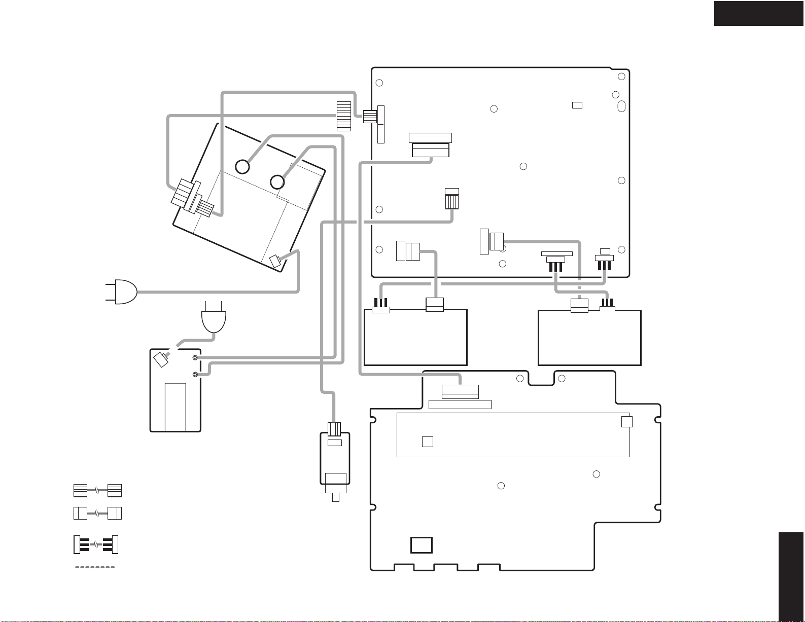
TA-RW255
PC BOARD CONNECTION DIAGRAM
Except <MDD>
JL901A
U03
POWER SUPPLY
PC BOARD
NAPS-8557
<MDD> only
Except <MDD>
P902
JL902A
<MDD>
U01
JL902B
P801A
CASSETTE MECHA.-A CASSETTE MECHA.-B
MAIN BOARD NAAF-8555
P701A
P702A
P802A
P102A
P205
L G R
P101A
U05 POWER SWITCH PC BOARD
NASW-8559
JUMPER WIRE
FLAT CABLE
U04 INPUT VOLUME
PC BOARD
SOCKET
BOARD TO BOARD
NAETC-8558
P701B
P702
U02
DISPLAY CIRCUIT PC BOARD NADIS-8313
TA-RW255
Page 13
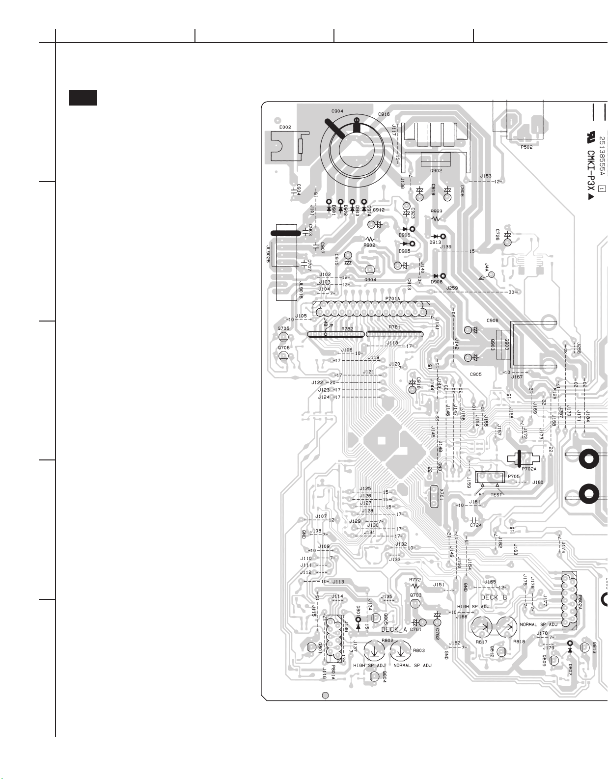
PRINTED CIRCUIT BOARD VIEWS-1
A
1
2
3
4
5
BCDEFGH
U01
MAIN PC BOARD
(NAAF-8555)
Component side view
from soldering side
Page 14
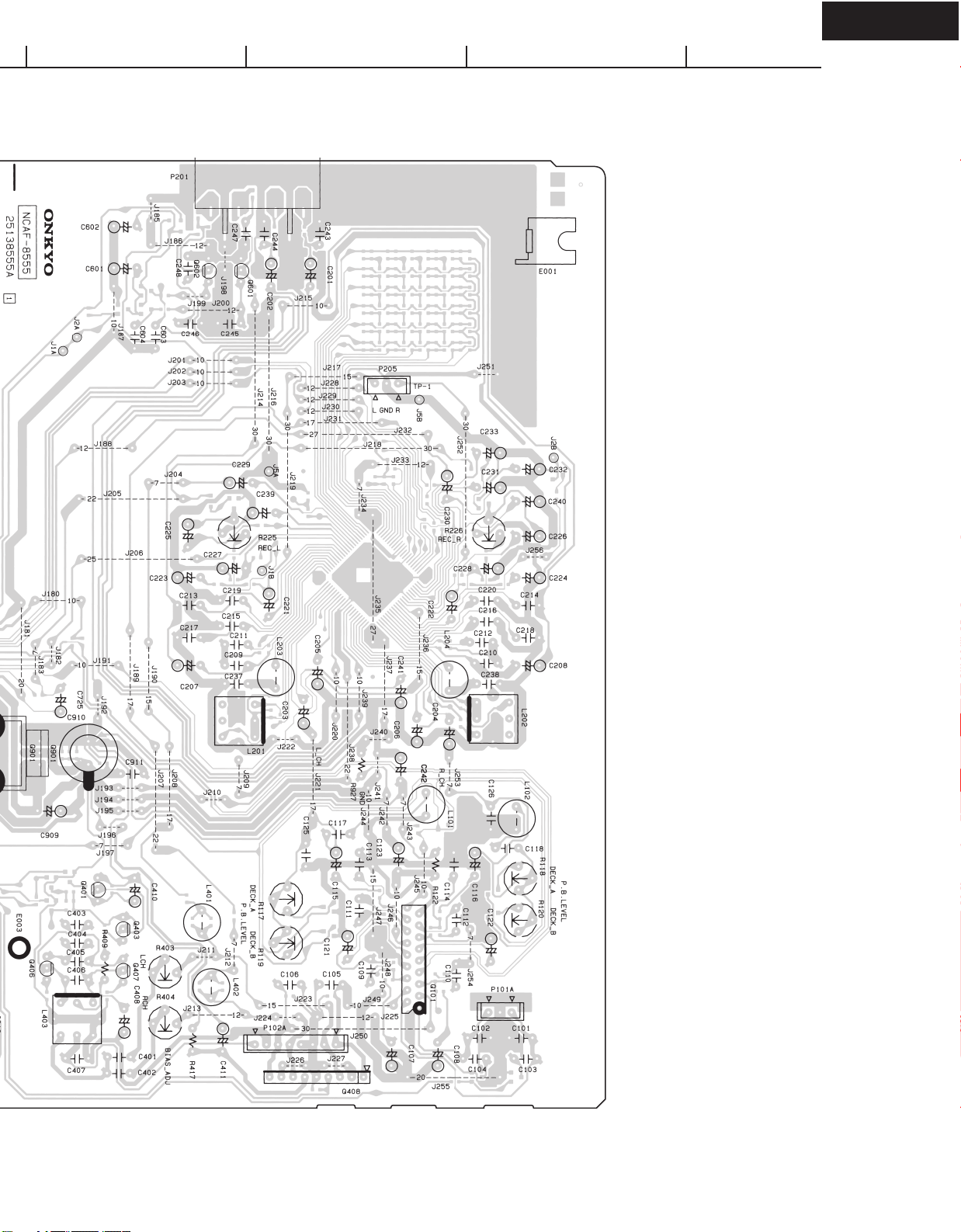
TA-RW255
Page 15
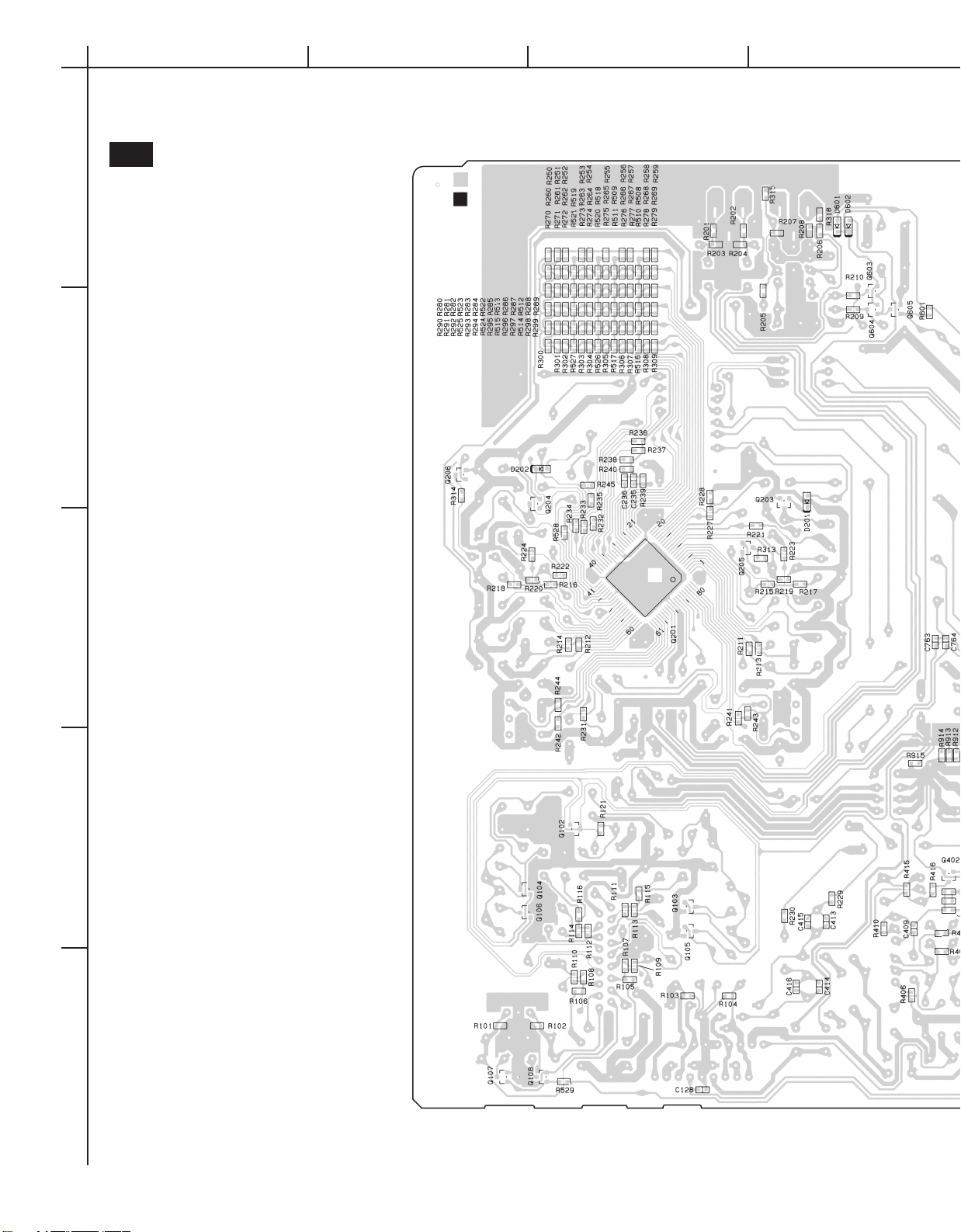
PRINTED CIRCUIT BOARD VIEWS-2
A
1
2
3
4
5
BCDEFGH
Soldering side view
U01
MAIN PC BOARD
(NAAF-8555)
Page 16
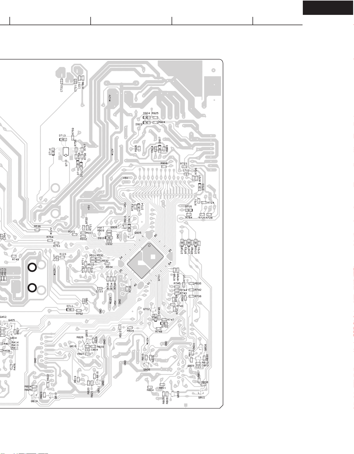
TA-RW255
Page 17
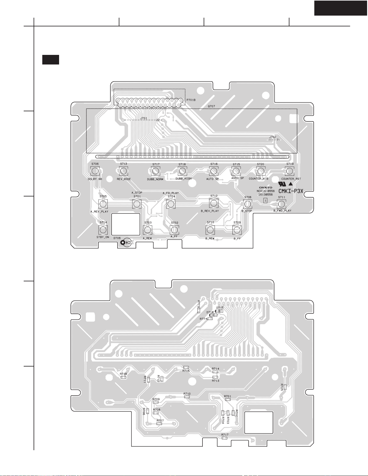
TA-RW255
A
PRINTED CIRCUIT BOARD VIEWS-3
U02
1
2
DISPLAY CIRCUIT PC BOARD (NADIS-8556)
Component side view from soldering side
BCD
3
Soldering side
4
5
Page 18
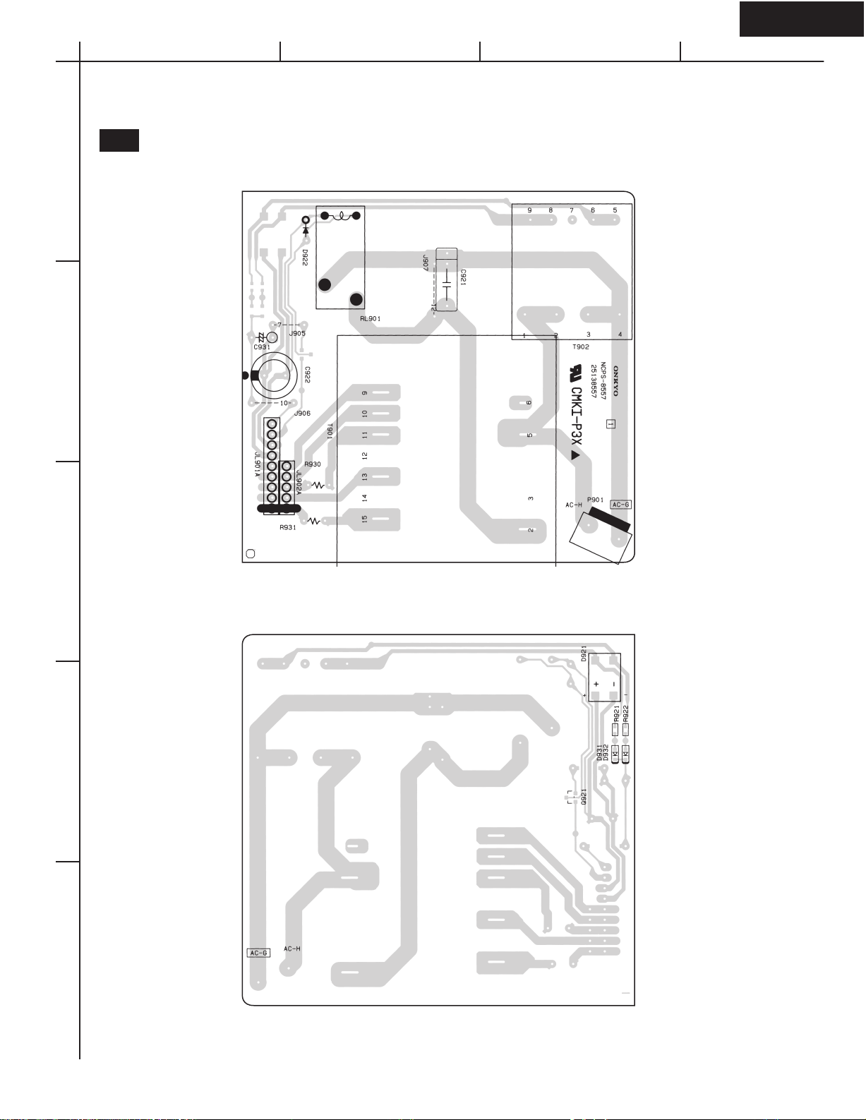
TA-RW255
A
PRINTED CIRCUIT BOARD VIEWS-4
U03
1
2
POWER SUPPLY PC BOARD (NAPS-8557)
Component side view from soldering side
BCD
3
Soldering side
4
5
Page 19
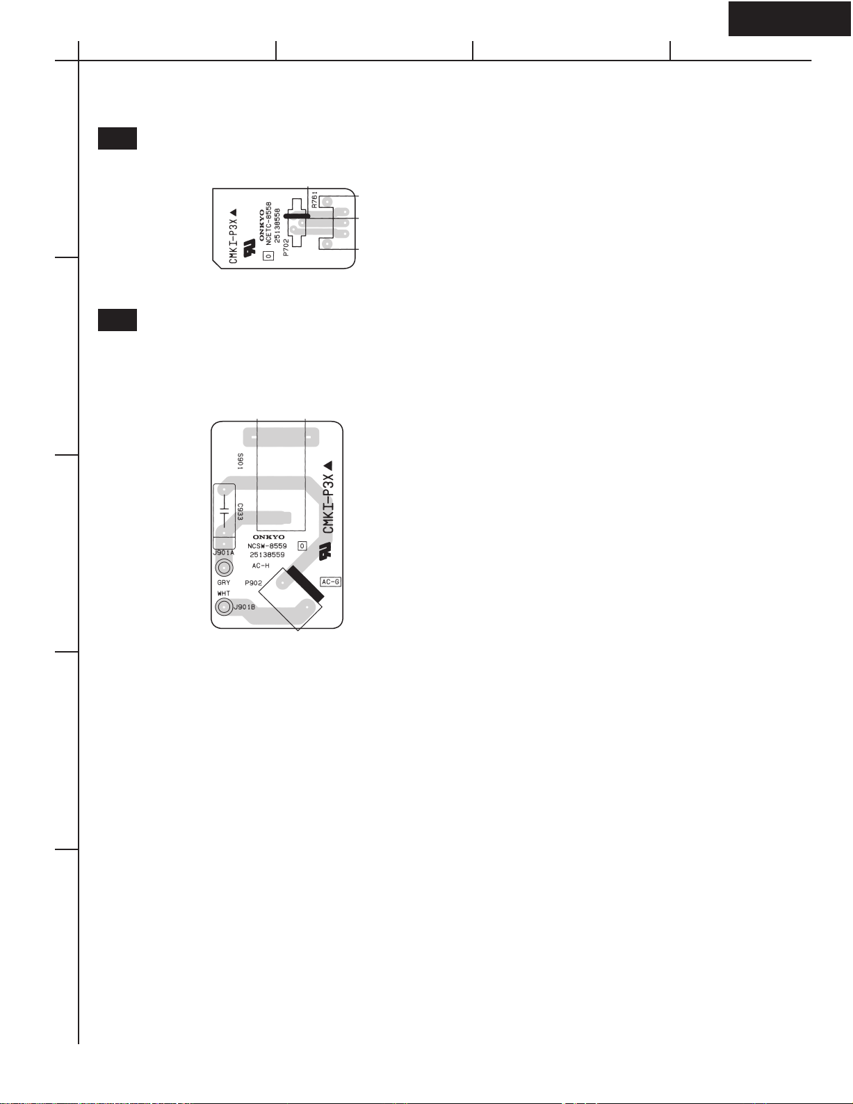
TA-RW255
A
PRINTED CIRCUIT BOARD VIEWS-5
U04
1
U05
2
INPUT VOLUME PC BOARD (NAETC-8558)
Component side view from soldering side
POWER SWITCH PC BOARD (NASW-8559)
EXCEPT <MDD>
Component side view from soldering side
BCD
3
4
5
Page 20
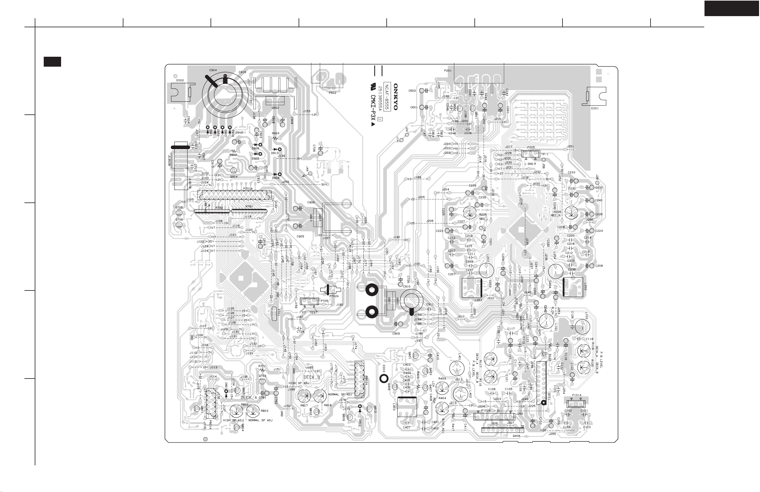
TA-RW255
PRINTED CIRCUIT BOARD VIEWS-1
A
1
2
3
4
5
BCDEFGH
U01
MAIN PC BOARD
(NAAF-8555)
Component side view
from soldering side
Page 21
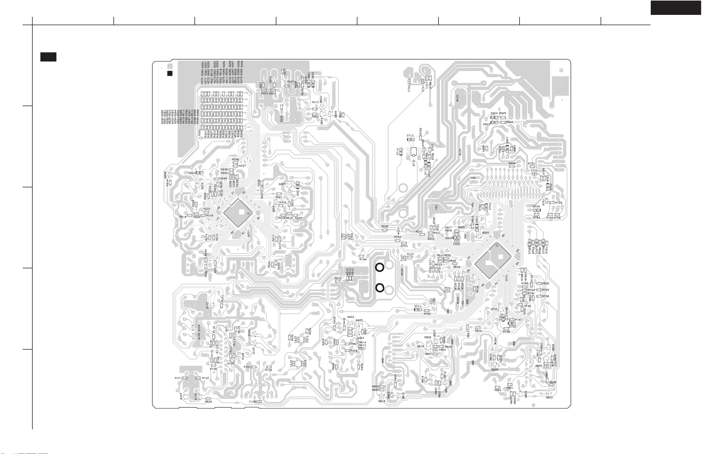
TA-RW255
PRINTED CIRCUIT BOARD VIEWS-2
A
1
2
3
4
5
BCDEFGH
Soldering side view
U01
MAIN PC BOARD
(NAAF-8555)
Page 22
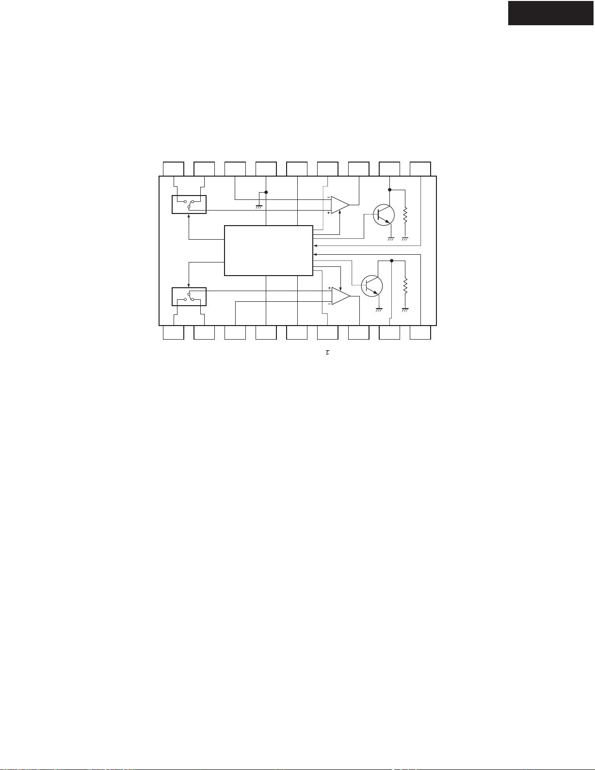
IC BLOCK DIAGRAM/ TERMINAL DESCRIPTION
Q101 : BA3416BL DUAL PLAYBACK PRE_AMPLIFIER
TA-RW255
IN
2-AIN2-B
NF2
GND FILTER OUT 2
VCC
METAL
IN 2
TAPE
A
2 4 6 8 10 12 14 16 18
GND
CONTROL
MUTE
A
A
100 k ohm 100 k ohm
1357911131517
IN
1-AIN1-B
NF1
TAPE_A
METAL
TAPE_B
METAL
OUT 1
METAL
IN 1
TAPE
B
Page 23

HA12167FB/HA12169FB
Audio Signal Processor for Cassette Deck (Deck 1 Chip)
ADE-207-110B (Z)
3rd Edition
Description
HA12167FB/HA12169FB is silicon monolithic bipolar IC providing REC volume system, Level meter
system and Dolby noise reduction system* in one chip.
Functions
• REC equalizer × 2 channel
• Equalizer volume × 2 channel
• Dolby B/C NR × 2 channel
• REC/PB input electronic volume × 2 channel
• Level Meter × 2 channel
• DAC for adjusting bias × 2 channel
Features
• Available to create characteristics of REC equalizer by changing external resistor, no coil
• Equalizer volume is available to calibrate recording automatically with micro-controller
• Electronic volume built-in is available to set the level of recording and play back automatically with
micro-controller
• 4 types of input (3 out of 4 are by way of electronic volume)
• Input electronic control switching is irrelevant to REC/PB electronic control switching
• Dolby noise reduction system is available with double cassette decks (Unprocessed signal output
available from recording out terminals during PB mode)
• Log-compressed level meter output is range from 0 V to 5 V (Usable as music search switchable gain of
0 dB and 20 dB respectively)
• Normal-speed/high-speed, normal/metal/chrome fully electronic control switching built-in
• NR-ON/OFF, Dolby B/C, MPX ON/OFF fully electronic control switching built-in
• Reduction of the number of pins by transfered serial data to electronic volume control switching and
another control switching (Controllable from micro-controller directly)
• Small the number of external parts
Page 24

HA12167FB/HA12169FB
Ordering Information
Operating Voltage
Type Package PB-OUT Level REC-OUT Level Dolby Level Min Max
HA12167FB QFP-80 775 mVrms 300 mVrms 300 mVrms 12.0 V 15.0 V
HA12169FB (14 × 14) 580 mVrms 11.0 V 15.0 V
* Dolby is a trade mark of Dolby Laboratories Licensing Corporation.
A license from Dolby Laboratories Licensing Corporation is required for the use of this IC.
2
Page 25
HA12167FB/HA12169FB
Pin Description (VCC = 14 V, Ta = 25°C, No signal, The value in the show typical
value.)
Pin No.
(QFP-80)
65 RPI 100 k VCC/2 Recording input
76
9 LM IN 100 k Level meter input
52
12 EQ IN 100 k Equalizer input
49
66, 67, 69 VRI 100 k VCC/2 + 0.7 V Volume input
72, 74, 75
30, 31 VCC — V
77 REF — VCC/2 — Ripple filter
62 NR IN — VCC/2 NR processor
Terminal
Name Zin DC Voltage Equivalent Circuit Description
CC
— Power supply
input
79
3 SS 1 — VCC/2 Spectral skewing
amp input
58
5 CCR — VCC/2 Current controlled
resistor output
56
3
Page 26
HA12167FB/HA12169FB
Pin Description (VCC = 14 V, Ta = 25°C, No signal, The value in the show typical
value.) (Cont)
Pin No.
(QFP-80)
63 IA OUT — VCC/2
78
61 VREF Reference voltage
80 buffer output
2 PB OUT Play back
59 (Decode) output
4 SS 2 Spectal skewing
57 amp. output
8 REC OUT Recording
53 (Encode) output
15 EQ OUT Equalizer output
46
1 TP 1.5 k VCC/2
Terminal
Name Zin DC Voltage Equivalent Circuit Description
V
CC
GND
+
–
Input amp output
Bias trap terminal
60
6 HLS DET — 2.3 V Time constant pin
for rectifier
55
7 LLS DET
54
4
Page 27
HA12167FB/HA12169FB
Pin Description (VCC = 14 V, Ta = 25°C, No signal, The value in the show typical
value.) (Cont)
Pin No.
(QFP-80)
64 BIAS — 0.28 V
14 IREF — 1.2 V EQ reference
27 MF EQ parameter
26 fQ current input
25 f/Q
24 GH
23 GL
22 GP
35 BIAS ADJ (N) — 1.2 V Bias DAC
36 BIAS ADJ (M) parameter current
37 BIAS ADJ (C) input
21 HM — —
Terminal
Name Zin DC Voltage Equivalent Circuit Description
Dolby NR
reference current
input
GND
current input
EQ parameter
selector
20 HC
19 HN
18 NM
17 NC
16 NN
GND
5
Page 28
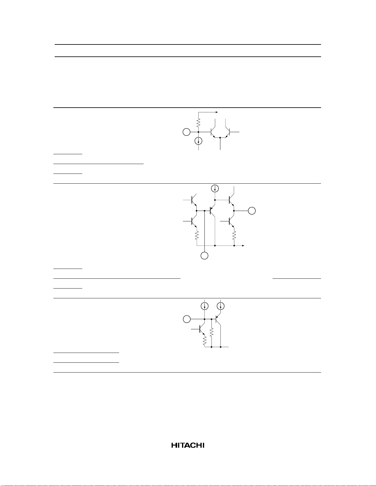
HA12167FB/HA12169FB
Pin Description (VCC = 14 V, Ta = 25°C, No signal, The value in the show typical
value.) (Cont)
Pin No.
(QFP-80)
68 CONT 3.3 k VCC/2 – 1.5 V
73
13 EQ CONT 1.65 k
48
10 LM DET — 0.2 V
51
11 LM OUT — 0.2 V Level meter output
50
45 NR ON/OFF 100 k —
Terminal
Name Zin DC Voltage Equivalent Circuit Description
DAC output
volume control
input
Time constant pin
for level meter
Mode control time
constant
to V
V /2
/2
CC
DAC
OUT
LM DET
CC
LM
OUT
GND
44 C/B
43 MPX
6
GND
Page 29
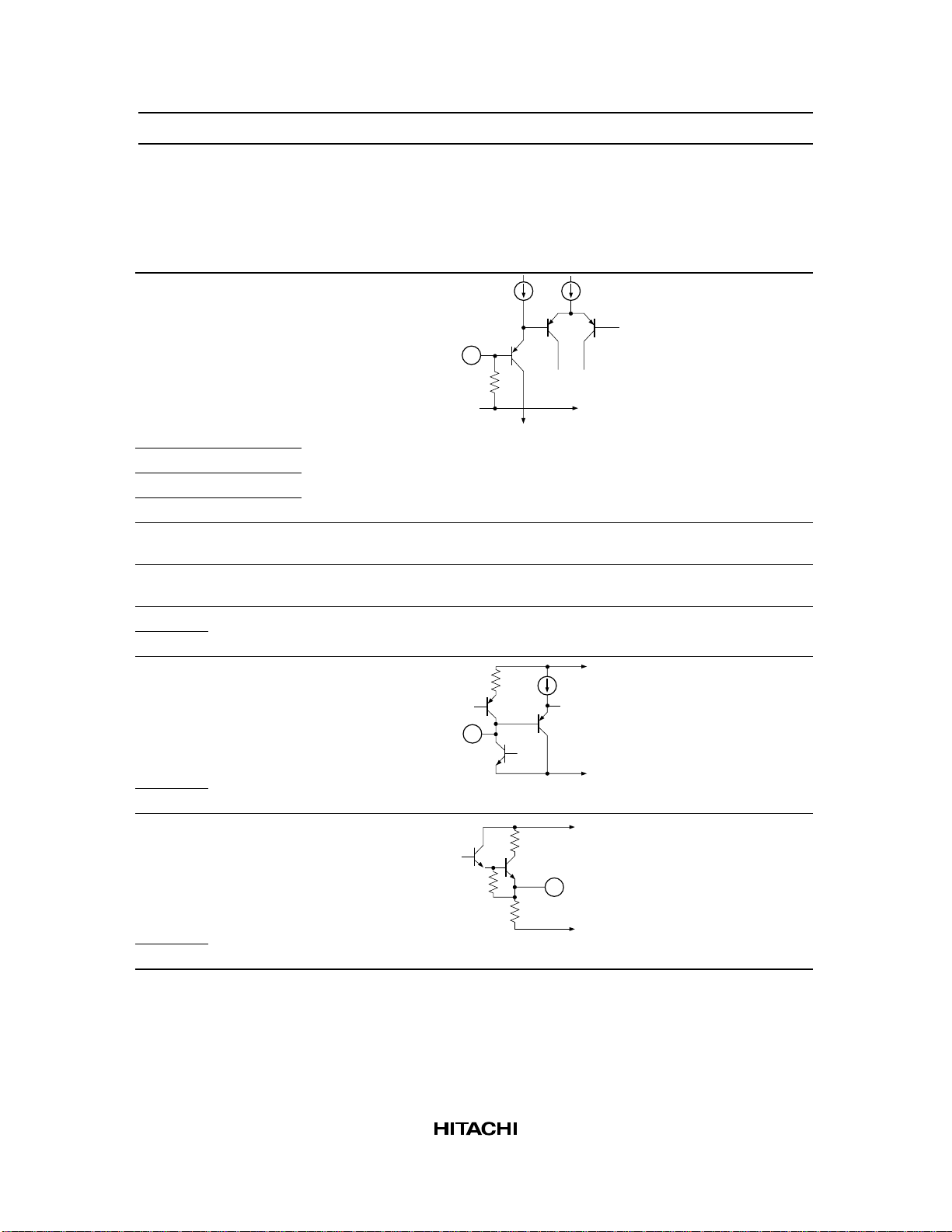
HA12167FB/HA12169FB
Pin Description (VCC = 14 V, Ta = 25°C, No signal, The value in the show typical
value.) (Cont)
Pin No.
(QFP-80)
42 RESET 100 k —
41 STB
40 DATA
39 CLK
38 INJ — 0.7 V — Injection current
47 D-GND — 0.0 V — Digital (Logic)
70 GND — 0.0 V — Ground
71, 34
28 BIAS CONT — —
Terminal
Name Zin DC Voltage Equivalent Circuit Description
Mode control input
D•GND
GND
2
input I
L
ground
V
CC
Bias DAC output
33
29 DAC OUT — —
32
GND
V
CC
GND
Bias DAC buffer
out
7
Page 30
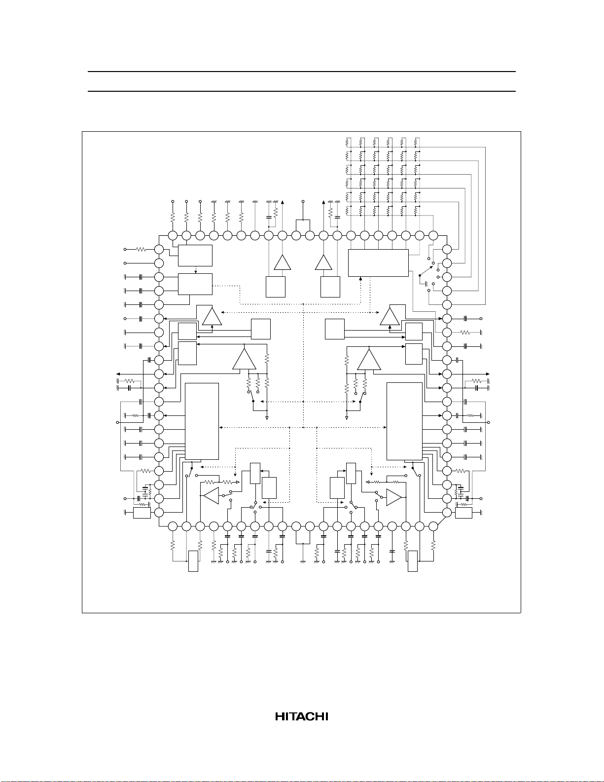
HA12167FB/HA12169FB
Block Diagram
EQ
EQ
LM
LM
LM
REC
LLS
HLS
RESET
NR
ON/
(L)
OUT
(L)
CONT
(L)
OUT
(L)
DET
IN
(L)
(L)
OUT
(L)
DET
(L)
DET
(L)
CCR
(L)
SS2
PBOUT
TP
STB
C/B MPX
OFF
D-GND
EQ
SS1
(L)
(L)
DATA
40
CLK
39
IIL
SW
INJ
38
LOGIC
BIAS ADJ (C)
BIAS ADJ (M)
BIAS ADJ (N)
37
36
35
GND
BIAS CONT (L)
34
33
6BIT
CC
DAC OUT (L)
V
32
31
DAC
DAC OUT (R)
30
29
BIAS CONT (R)
FMfQf/Q
28
6BIT
DAC
GHGLGP
27
26
25
24
HM
23
22
21
2019181716151413121110987654321
EQ-CONTROLER
NN NC NM HN HC
(R)
EQ
TRAP
BIAS
IN
SS1
(R)
(R)
IREF
EQ
OUT
EQ
CONT
LM
OUT
LM
DET
IN
LM
REC
OUT
LLS
DET
HLS
DET
(R)
CCR
(R)
SS2
(R)
PBOUT
TP
(R)
(R)
(R)
(R)
(R)
(R)
(R)
(R)
EQ
REC
5BIT
5BIT
EQ
VOL
IN
(L)
RECT
DAC
LMA
–
+
DAC
DOLBY B/C NR
(L)
IA
TRAP
BIAS
60 59 58 57 56 55 54 53 52 51 50 49 48 47 46 45 44 43 42 41
61
62
63
64
E. VOL
6BIT
DAC
65
66
67
68
69
70
71
E. VOL
6BIT
DAC
72
73
74
EQ
REC
EQ
VOL
LMA
–
+
RECT
DOLBY B/C NR
IA
75
76
77
78
79
80
Vref (L)
MPX
NRIN (L)
IA OUT (L)
BIAS
RPI (L)
VRI 3 (L)
VRI 2 (L)
VRI 1 (L)
CONT (L)
GND
VRI 1 (R)
CONT (R)
VRI 2 (R)
VRI 3 (R)
RPI (R)
REF
MPX
NRIN (R)
IA OUT (R)
Vref (R)
8
Page 31

HA12167FB/HA12169FB
Absolute Maximum Ratings
Item Symbol Rating Unit Note
Supply voltage V
Power dissipation Pd 750 mW 1
Operating temperature Topr –30 to +75 °C
Storage temperature Tstg –55 to +125 °C
Note: For Ta is higher than 65°C, reduce Pd at the rate of 12.5 mW/°C.
Please, see the below graph.
max 15 V
CC
[mW]
750
625
Pd
–30 65 75
Ta [°C]
9
Page 32

10
Test Conditions
—————————————————————————————————————
Specification REC
——————– REC RV Input Tape Input EQ Bias fin OUT
Item Symbol Min Typ Max Unit /PB /PV MPX NR B/C Pin Meter Speed Tape DAC DAC DAC [Hz] Level
——————————————————————————————————————————————————————————————————–
Quiescent current IQ — 34.5 42.0 mA PB PV OFF OFF B VRI1 NOR NOR NOR 32 0 0 — — No signal
———————————————————————————————————————————————————————————
Input amp. gain GVIA 18.5 20.0 21.5 dB REC RV ON OFF B RPI NOR NOR NOR 63 0 0 1 k 0
RPI
———————————————————————————————————————————————————————————
B-type encode B-ENC 2.8 4.3 5.8 dB REC RV ON OFF B RPI NOR NOR NOR 63 0 0 2 k –20
boost -2 k
→
ON
————————–
———————————————————————————————————————————–
B-ENC 1.7 3.2 4.7 REC RV ON OFF B RPI NOR NOR NOR 63 0 0 5 k –20
-5 k
→
ON
———————————————————————————————————————————————————————————
C-typ encode C-ENC 3.9 5.9 7.9 dB REC RV ON OFF C RPI NOR NOR NOR 63 0 0 1 k –20
boost -1 k (1)
→
ON
————————–
———————————————————————————————————————————–
C-ENC 18.1 19.6 21.6 REC RV ON OFF C RPI NOR NOR NOR 63 0 0 1 k –60
-1 k (2)
→
ON
————————–
———————————————————————————————————————————–
C-ENC 9.8 11.8 13.8 REC RV ON OFF C RPI NOR NOR NOR 63 0 0 700 –30
-700
→
ON
———————————————————————————————————————————————————————————
Signal handling VOMax 12.0 13.0 — dB REC RV ON ON C RPI NOR NOR NOR 63 0 0 1 k —
———————————————————————————————————————————————————————————
Signal to noise S/N (C) 60.0 63.0 — dB REC RV ON ON C RPI NOR NOR NOR 63 0 0 — — Rg = 5.1 kΩ
ratio CCIR/ARM
———————————————————————————————————————————————————————————
T.H.D. THD (C) — 0.08 0.3 % REC RV ON ON C RPI NOR NOR NOR 63 0 0 1 k 0
———————————————————————————————————————————————————————————
Crosstalk CT — –85.0 –79.0 dB REC RV ON OFF B VPI1 NOR NOR NOR 0 0 0 1 k 6
(R
←→
L)
————————–
———————————————————————————————————————————–
CT — –80.0 –74.0 REC RV ON OFF B VRI1 NOR NOR NOR 0 0 0 1 k 6
(VRI1
←→
←→
VRI2) VRI2
————————–
———————————————————————————————————————————–
CT — –80.0 –74.0 REC RV ON OFF B VRI1 NOR NOR NOR 0/63 0 0 1 k 6
(VRI1
←→
←→
RPI) RRI
———————————————————————————————————————————————————————————
Application Terminal
—————————
Input Output
———– ———–
R L R L Note
————30
31
76 65 78 63
76 65 8 53
76 65 8 53
76 65 8 53
76 65 8 53
76 65 8 53
76 65 8 53 1
76 65 8 53
76 65 8 53
72 69 8 53
72/ 69/ 2 59
74 67
72/ 69/ 2 59
76 65
Electrical Characteristics (Ta = 25°C, V
RECOUT)
HA12167FB/HA12169FB
CC
= 14 V, Dolby Level 300 mVrms at
Page 33

Electrical Characteristics (Ta = 25°C, V
Test Conditions
—————————————————————————————————————
Specification REC
——————– REC RV Input Tape Input EQ Bias fin OUT
Item Symbol Min Typ Max Unit /PB /PV MPX NR B/C Pin Meter Speed Tape DAC DAC DAC [Hz] Level
——————————————————————————————————————————————————————————————————–
Serial digital VSH 4.0—5.3V ——————————————CLK, DATA, STB
input level
—————————— ———————————————————————————– ——————–
VSL –0.2 — 1.0 — — ————————————
———————————————————————————————————————————————————————————
PB- Vout 500 580 670 mVrms REC RV ON OFF B RPI NOR NOR NOR 63 0 0 1 k 0
output
——– —————–
level 665 775 900
———————————————————————————————————————————————————————————
PB-out offset Vofs –100 0.0 +100 mV PB PV OFF OFF C RPI NOR NOR NOR 63 0 0 — — No signal
→
ON
———————————————————————————————————————————————————————————
Channel balance ∆Gv –1.0 0.0 1.0 dB — — ————————————
———————————————————————————————————————————————————————————
REC volume gain GVrec VR 17.5 19.1 21.5 dB REC RV ON OFF B VRI1 NOR NOR NOR 0 0 0 1 k — Vin = 100 mVrms
(Max)
——————————————————————————————————————————————————————
GVrec VR –56.0 –50.0 –47.0 dB REC RV ON OFF B VRI1 NOR NOR NOR 62 0 0 1 k — Vin = 2 Vrms
(Min)
———————————————————————————————————————————————————————————
PB volume gain G
V PB
VR 27.0 29.0 31.0 dB PB PV ON OFF B VRI1 NOR NOR NOR 0 0 0 1 k — Vin = 100 mVrms
(Max)
——————————————————————————————————————————————————————
G
V PB
VR 15.0 17.0 19.0 dB PB PV ON OFF B VRI1 NOR NOR NOR 62 0 0 1 k — Vin = 100 mVrms
(Min)
———————————————————————————————————————————————————————————
REC volume mute CTrec VR — –82 –75 dB REC RV ON OFF B VRI1 NOR NOR NOR 63 0 0 1 k — Vin = 2 Vrms
level (MUT)
———————————————————————————————————————————————————————————
REC volume max Vin max 11.0 12.0 — dBS REC RV ON OFF B VRI1 NOR NOR NOR 42 0 0 1 k — THD = 1%
input level (VR)
———————————————————————————————————————————————————————————
Signal to noise S/N (VR) 78.0 84.0 — dB REC RV ON OFF B VRI1 NOR NOR NOR — 0 0 (1 k) 0 Vin = 100 mVrms
ratio of REC Rg = 5.1 k, A-WTG
volume
———————————————————————————————————————————————————————————
T.H.D. of REC THD (VR) — 0.04 0.3 % REC RV ON OFF B VRI1 NOR NOR NOR — 0 0 1 k 0 Vin = 100 mVrms
volume
———————————————————————————————————————————————————————————
Application Terminal
—————————
Input Output
———– ———–
R L R L Note
————39
40
————41
76 65 2 59
——2 59 2
76 65 78 63
72 69 78 63
72 69 78 63
72 69 78 63
72 69 78 63
72 69 2 59
72 69 2 59
72 69 2 59 3
72 69 2 59 3
High
Low
HA12169
HA12167
RECOUT) (Cont)
11
CC
= 14 V, Dolby Level 300 mVrms at
HA12167FB/HA12169FB
Page 34

12
Test Conditions
—————————————————————————————————————
Specification REC
——————– REC RV Input Tape Input EQ Bias fin OUT
Item Symbol Min Typ Max Unit /PB /PV MPX NR B/C Pin Meter Speed Tape DAC DAC DAC [Hz] Level
——————————————————————————————————————————————————————————————————–
Equalizer gain GVEQ 23.5 25.5 27.5 dB REC RV ON OFF B RPI NOR NOR NOR 63 0 0 500 — Vin = –32 dBs
(500)
————————–
———————————————————————————————————————————–
GVEQ 23.5 25.5 27.5 REC RV ON OFF B RPI NOR NOR NOR 63 0 0 1 k — Vin = –32 dBs
(1 k)
————————–
———————————————————————————————————————————–
GVEQ 25.0 27.0 29.0 REC RV ON OFF B RPI NOR NOR NOR 63 0 0 5 k — Vin = –32 dBs
(5 k)
————————–
———————————————————————————————————————————–
GVEQ 31.0 33.5 36.0 REC RV ON OFF B RPI NOR NOR NOR 63 0 0 12 k — Vin = –32 dBs
(12 k)
———————————————————————————————————————————————————————————
Equalizer volume ∆GVEQ 6 8 10 dB REC RV ON OFF B RPI NOR NOR NOR 63 0/30 0 1 k — Vin = –32 dBs
variable a range (1 k)
———————————————————————————————————————————————————————————
Equalizer max Vin Max –10.0 –9.0 — dBS REC RV ON OFF B RPI NOR NOR NOR 63 16 0 1 k — THD = 1%
input level (EQ)
———————————————————————————————————————————————————————————
Equalizer volume GVEQ — –75 –62 dB REC RV ON OFF B RPI NOR NOR NOR 63 31 0 1 k — Vin = –9 dBs
mute gain (MUT) 1 kHz BPF
———————————————————————————————————————————————————————————
Signal to noise S/N (EQ) 57.0 62.0 — dB REC RV ON OFF B RPI NOR NOR NOR 63 0 0 — — Rg = 5.1 kΩ, A-WTG
radio of equalizer
———————————————————————————————————————————————————————————
THD of equalizer THD (EQ) — 0.2 0.5 % REC RV ON OFF B RPI NOR NOR NOR 63 16 0 1 k — Vin = –26 dBs
———————————————————————————————————————————————————————————
Equalizer offset Vofs (EQ) –400 0.0 +400 mV REC RV OFF OFF B RPI NOR NOR NOR 63 0 0 — — No signal
———————————————————————————————————————————————————————————
Level meter LM 2.50 2.75 3.00 V REC RV ON OFF B RPI NOR NOR NOR 63 0 0 1 k 0
output (0 dB)
——————————————————————————————————————————————————————
LM 3.55 3.85 4.15 V REC RV ON OFF B RPI NOR NOR NOR 63 0 0 1 k 12
(12 dB)
——————————————————————————————————————————————————————
LM 0.70 1.00 1.30 V REC RV ON OFF B RPI NOR NOR NOR 63 0 0 1 k –20
(–20 dB)
1
——————————————————————————————————————————————————————
LM 2.45 2.75 3.05 V REC RV ON OFF B RPI 20 dB NOR NOR 63 0 0 1 k –20
(–20 dB)
2
———————————————————————————————————————————————————————————
Application Terminal
—————————
Input Output
———– ———–
R L R L Note
12 49 15 46
12 49 15 46
12 49 15 46
12 49 15 46
12 49 15 46
12 49 15 46
12 49 15 46
12 49 15 46
12 49 15 46
— — 15 46 4
9521150
9521150
9521150
9521150
HA12167FB/HA12169FB
Electrical Characteristics (Ta = 25°C, V
RECOUT) (Cont)
CC
= 14 V, Dolby Level 300 mVrms at
Page 35

Electrical Characteristics (Ta = 25°C, V
Test Conditions
—————————————————————————————————————
Specification REC
——————– REC RV Input Tape Input EQ Bias fin OUT
Item Symbol Min Typ Max Unit /PB /PV MPX NR B/C Pin Meter Speed Tape DAC DAC DAC [Hz] Level
——————————————————————————————————————————————————————————————————–
Level meter offset LMofs 1 — 150 300 mV REC RV ON OFF B RPI NOR NOR NOR 63 0 0 — — No signal
————————–
———————————————————————————————————————————–
LMofs 2 — 200 350 REC RV ON OFF B RPI 20 dB NOR NOR 63 0 0 — — No signal
———————————————————————————————————————————————————————————
DAC output Max VBMax 11.0 12.0 13.0 V REC RV OFF OFF B VRI1 NOR NOR MET 63 0 63 — —
———————————————————————————————————————————————————————————
DAC output Min VBMin — 0.5 1.0 V REC RV OFF OFF B VRI1 NOR NOR MET 63 0 0 — —
——————————————————————————————————————————————————————————————————–
Note: 1. HA12167: VCC= 12 V
HA12169: V
CC
= 11 V
2. V
CC
= 15 V
3. Adjust the input volume to Dolby level.
4. V
CC
= 15 V
Application Terminal
—————————
Input Output
———– ———–
R L R L Note
——1150
——1150
— — 29 32
— — 29 32
RECOUT) (Cont)
13
CC
= 14 V, Dolby Level 300 mVrms at
HA12167FB/HA12169FB
Page 36

HA12167FB/HA12169FB
Test Circuit
C41
100µ
+
CC
V
MODE
CONTROLLER
CC
V
10k
R12
1µ
C14
+
R13
100k
35 34 33 32 31
33k
R14
36
20k
R15
37
24k
R16
+5V
C45C46C47
4
10k
R21
GND
Digital
51k
R22
R23
100k
1µ
C21
47k
R25
R24
7.5k
12k
R79
C29
2.2µ
2200p 2200p
+
10k
R28
38
R17
1.2k
10P10P10P
22k
R18
40 39
22k
R19
41
22k
R20
22k
R80
+++
C15
4.7µ
44 43 42
C16
4.7µ
45
C17
4.7µ
46
+
C18
2.2µ
47
48
++
1µ
C19
C20
0.47µ
49
51 50
+
C22
0.1µ
52
+
C23
2.2µ
C24
0.1µ
C25
0.1µ
56 55 54 53
C26
2200p
57
560
R26
C27 C28
22k
R27
59 58
60
R29
5.6k
62 61
DAC OUT(L)
BIAS CONT(L)
GND
BIAS ADJ(N)
BIAS ADJ(M)
BIAS ADJ(C)
INJ
CLK
DATA
STB
RESET
MPX
C/B
NR ON/OFF
EQOUT(L)
DGND
EQCONT(L)
EQIN(L)
LMOUT(L)
LMDET(L)
LMIN(L)
RECOUT(L)
HA12167/HA12169 (REC 1 CHIP)
LLSDET(L)
HLSDET(L)
CCR(L)
SS2(L)
SS1(L)
PB OUT(L)
TP(L)
Vref(L)
NR IN(L)
IAOUT(L)
R30
2.4k
BIAS
64 63
18k
R31
+++
C30
R32
5.1k
C31
10k
R33
C32
10k
R34
++
C33
C34
R35
5.1k
RPI(L)
65
0.47µ
VRI3(L)
0.47µ
VRI2(L)
0.47µ
1µ
0.47µ
CONT(L)
VRI1(L)
GND
70 69 68 67 66
CC
V
3029
DAC OUT(R)
BIAS CONT(R)
28
FM
27
fQ
26
f/Q
25
GH
24
GL
23
R47 R46 R45 R44 R43 R42
GP
22
HM
21
HC
20
NH
1918171615141312
NM
NC
NN
EQOUT(R)
IREF
EQCONT(R)
EQIN(R)
LMOUT(R)
1110
LMDET(R)
LMIN(R)
9
RECOUT(R)
8
LLSDET(R)
7
HLSDET(R)
654
CCR(R)
SS2(R)
R3
SS1(R)
3
R2
PB OUT(R)
2
TP(R)
1
Vref(R)
80
NR IN(R)
79
IAOUT(R)
787372
REF
RPI(R)
76 77
VRI3(R)
75
VRI2(R)
74
C37 C38 C39 C40
CONT(R)
C36
VRI1(R)
GND
71
10k
R11
+
R48R49R50R51R52R53
R54R55R56R57R58R59
C12
2.2µ
+
1µ
C11
+
C10
0.47µ
+
+
C8
0.1µ
R4
+
C7
2.2µ
C6
0.1µ
C5
0.1µ
C4
2200p
560
C2 C3
22k
2200p 2200p
R41
5.6k
R40
2.4k
C39
+
0.47µ 0.47µ 0.47µ 1µ
+++++
1µ
C35
0.47µ
R36
R10
100k
1µ
C13
R60R61R62R63R64R65
R66R67R68R69R70R71
R72R73R74R75R76R77
33k 33k 33k 51k 51k 100k
R9
10k
R8
24k
R7
51k
R6
100k
1µ
C9
R5
7.5k
47k
12k
R78
C1
2.2µ
+
R1
10k
R39
5.1k
10k
R38
10k
R37
5.1k
AGND DGND
14
Page 37

Mode Controller
A
HA12167FB/HA12169FB
R8
C2
GND VCC(+5V)
VCC
1 RST
JP1
1M
Q
Q
+
2.2µ
R7
+
CLR
22k
R6
22k
SW16
N8 IC11
R5
22k
R9
22k
Z
R3
1M
+
C1
2.2µ
C3
100µ
R2
22k
PR
R1
PR
Q
R29
IC1
N1 IC2
Q
Q
JP2
22k
22k
Q
D
Q
D
Q
D13 IC4
CLR
CLR
CLR
6 GND
5
R27
22k
D10
IC11
ABCD
QQQQ
CLR
D15 IC12 D7 IC5 D6 IC5 D5 IC6
N9 IC11
R26
22k
D2 IC3
D1 IC3
TRIGGER
IC 1
SW15
D3 IC12
Q
PR
D4 IC6
Q
PR
Q
PR
Q
PR
Q
PR
Q
PR
Q
CLR
D
Q
CLR
D
Q
CLR
D
Q
CLR
D
Q
CLR
D
Q
CLR
D
N12 IC11 N13 IC11
X'tal OSC
N2 IC2
MCLK
D12 IC4
CLK
3
CLR
R9
ABCD
QQQQ
R10
510
1M
X'tal
SW17
62.5kHz
N11 IC11N3 IC2
125kHz
C5
1MHz
C4
STB
4
250kHz
120P
30P
N5 IC10
500kHz
DAT
2
N4 IC2
N7 IC10
N6 IC10
R28
22k
D4 IC7
Q
Q
CLR
PR
D
Q
Q
CLR
PR
D
D9
IC7
A
R24
22k
B
R23
22k
C
R22
22k
D
R21
22k
EFGH
R20
22k
R19
22k
R18
22k
R17
22k
I
R16
22k
J
R15
22k
K
R14
22k
L
R13
22k
M
R12
22k
N
R11
22k
N8 IC10
SW1SW2SW3SW4SW5SW6SW7SW8
SW9
SW10SW11SW12SW13SW14
Serial
SHIFT
BCD E F G H
A CLK
Serial
SHIFT
CLK
ABCD E F G H
R25
22k
H
Q
.IN
LOAD
BIT
INHI
CLK
Q
.IN
HH
Q
LOAD
BIT
INHI
CLK
D10 IC8D11 IC9
Pin Name
RST
DATA
CLK
STB
VCC
Pin No.123456
Output connector CN1
CN3MNZGND
Pin Name
CN2EFGH
Pin No.5678
CN3IJKL
Pin Name
CN2ABCD
Pin No.1234
TTL Type
74HC221
74HC00
74HC74
74HC393
74HC165
IC No.12, 10
3, 5, 6, 7, 1248, 9
GND
74HC04
11
15
Page 38

HA12167FB/HA12169FB
Level Diagram
REC Mode (1 kHz NR-OFF)
EQOUT
EQIN
RECOUT
PBOUT
BIAS TRAP
TP
5.6k
E. VOL REC EQ
+
+
DOLBY - NR
1.5k
–1dBs
775mVrms
0dBs
–2.5dBs
HA12167
–5dBs
580mVrms
HA12169
–9dBs
–26dBs
0dBs = 775mVrms
–8.2dBs
300mVrms
–8.2dBs
* Input limit of VRI is more than 12dB on Vo max, and not variable range.
16
2.4k
MPX
VRI 1
NRIN VREF
IAOUT
IA
E. VOL
VRI 2
VRI 3
RPI
14k
6k
–5.2dBs
43mVrms
–25.2dBsRPI
–24.3
–20
dBs
–25
–30
–0.4dBs
0
VRI*
–5
–10
–15
Page 39

PB Mode (1 kHz NR-OFF)
HA12167FB/HA12169FB
EQOUT
EQIN
RECOUT
PBOUT
BIAS TRAP
TP
5.6k
E. VOL REC EQ
+
+
DOLBY - NR
1.5k
–1dBs
775mVrms
0dBs
(HA12167)
580mVrms
–2.5dBs
(HA12169)
–5dBs
–9dBs
–8.2dBs
300mVrms
–8.2dBs
0dBs = 775mVrms
–26dBs
2.4k
MPX
VRI 1
NRIN VREF
IAOUT
IA
E. VOL
VRI 2
VRI 3
RPI
14k
6k
–5.2dBs
–25.2
dBs
43mVrms
RPI
–28.2
–22.2dBs
0
–5
–10
–15
–20
dBs
–25
VRI
–30
–34.2
dBs
–35
17
Page 40

HA12167FB/HA12169FB
Application Note
Power Supply Range
HA12167FB/HA12169FB are designed to operate on either single supply or split supply.
The operating range of the supply voltage is shown in table 1.
Table 1 Supply Voltage
Type No. Single Supply Split Supply
HA12167FB 12 V to 15 V ±6.0 V to 7.5 V
HA12169FB 11 V to 15 V ±6.0 V to 7.5 V
The lower limit of supply voltage depends on the line output reference level.
The minimum value of the overload margin is specified as 12 dB by Dolby Laboratories. HA12167 series
are provided with two line output level, which will permit an optimum overload margin for power supply
conditions.
Reference Voltage
For the single supply operation these devices provide the reference voltage of half the supply voltage that is
the signal grounds. As the peculiarity of these devices, the capacitor for the ripple filter is very small about
1/100 compared with their usual value. The Reference voltage are provided for the left channel and the
right channel separately. The block diagram is shown as figure 1.
V
CC
+
–
77
+
1 µF
–
+
61
L channel
reference
R channel
reference
80
Figure 1 The Block Diagram of Reference Voltage Supply
18
Page 41

HA12167FB/HA12169FB
Operating Mode Control
HA12167FB/HA12169FB provides fully electronic switching circuits. All switches are controlled by serial
data.
Table 2 Threshold Voltage (VTH)
Pin No. Lo Hi Unit
42 –0.2 to 1.5 3.5 to 5.3 V
39, 40, 41 –0.2 to 1.0 4.0 to 5.3 V
Notes: 1. Voltages shown above are determined by internal circuits of LSI when take pin 47 (DGND pin) as
reference pin. On split supply use, same VTH can be offered by connecting DGND pin to GND
pin.
This means that it can be controlled directly by micro processor.
2. Each pins are on pulled down with 100 k internal resistor.
Therefore, it will be low-level when each pins are open.
3. Note on serial data inputting
(a) The clock frequency on CLK must be less than 500 kHz.
(b) Over shoot level and under shoot level of input signal must be the value shown below.
When connecting microcomputer or Logic-IC with HA12167FB/HA12169FB directly, there is
apprehension of rash-current under some transition timming of raising voltage or falling voltage at V
CC
ON/OFF.
For this countermeasure, connect 10 k to 20 k resistor with each pins. It is shown in test circuit on this
data sheet.
In case of changing NR-ON/OFF at the C-mode, for the countermeasure of the noise of pop, perform the
following processes.
In case of changing NR-OFF to NR-ON at C-mode. C-mode, NR-OFF → B-mode, NR-OFF → B-mode,
NR-ON → C-mode, NR-ON.
In case of changing NR-ON to NR-OFF at C-mode. C-mode, NR-ON → B-mode, NR-ON → B-mode,
NR-OFF → C-mode, NR-OFF.
19
Page 42

HA12167FB/HA12169FB
Under 5.3 V
0
Within –0.2 V
Figure 2 Input Level
Serial Data Formatting
14 bit shift register is employed.
CLK and data are stored during STB being high and data is latched when STB goes high to low.
Reset goes reset a state when reset low and high releasles reset. (High fixed at use time)
Attention Point of Serial Interface
• Reset goes low condition when a power supply is ON or OFF.
• Characteristics select of Bias DAC is connected with equalizer tape selector.
• Bias DAC register is all low when a time of tape select.
• Bias DAC register is all low and Bias DAC out is dropped low level at compulsion by force.
• Input pin select, REC/PB select and Input volume gain select does not select at the same time.
• Input volume must go mute condition when selected of RPI is input pin select.
CLK
DATA
STB
RESET
20
012345678910111213
Latch of data
Reset release
Figure 3 Serial Data Timming Chart Figure
Page 43

HA12167FB/HA12169FB
MUTE
DAC
BIAS CONT
+
Figure 4 Bias DAC Output Circuit
DACOUT
Buff
21
Page 44

HA12167FB/HA12169FB
Serial Data Formatting
Bit Mode Control Input Voltage Eaqualizer Voltage Basic DAC
No. Reset Reset Reset Reset
0 Tape
selector 1
1 Tape
selector 2
2 Tape
speed
3 Meter
sensitivity
4 Input
selector 1
5 Input
selector 2
6 REC/PB H PB mode selection H R
7 Input
voltage
gain
8 MPX H ON L I-bit 2 L E-bit 2 L B-bit 2 L
9 NR H ON L I-bit 3 L E-bit 3 L B-bit 3 L
10 B/C H C L I-bit 4 L E-bit 4 L B-bit 4 L
11 — — — I-bit 5 H — — B-bit 5 L
12 Registor
selector 1
13 Registor
selector 2
bit 0
bit 1 H L
H Metal Normal
L Crom Normal
H Hi speed selection L I-bit 2 L E-bit 2 L B-bit 2 L
L Normal speed selection
H Meter sensitivity 20 dBupL I-bit 3 L E-bit 3 L B-bit 3 L
L Meter sensitinity normal
bit 4
bit 5 H L
H VRI3 RPI
L VRI2 VRI1
L REC mode selection
H PB mode volume gain H I-bit 1 L E-bit 1 L B-bit 1 L
L Rec mode volume gain
L OFF
L OFF
L B
bit 12
bit 13 H L
H Bias DAC Input volume
L Equalizer volume Mode control
LL
channel
L I-bit 1 L E-bit 1 L B-bit 1 L
L I=bit 4 L E-bit 4 L B-bit 4 L
L I-bit 5 H — — B-bit 5 L
channel
I-bit 0 L L
I-bit 0 L R
channel
channel
E-bit 0 L L
E-bit 0 L R
B-bit o L
channel
B-bit 0
channel
22
Page 45

HA12167FB/HA12169FB
Input Volume Register
I-bit 5 I-bit 4 I-bit 3 I-bit 2 I-bit 1 I-bit 0 Gain
LLLLLLIncrease
LLLLLH↑
LLLLHL:
LLLLHH:
:::::::
::::::↓
HHHHHLDecrease
HHHHHHMute
Equalizer Volume Register
E-bit 4 E-bit 3 E-bit 2 E-bit 1 E-bit 0 Gain
LLLLLIncrease
LLLLH↑
LLLHL:
LLLHH:
::::::
:::::↓
HHHHLDecrease
HHHHHMute
Bias DAC Register
B-bit 5 B-bit 4 B-bit 3 B-bit 2 B-bit 1 B-bit 0 Bias
LLLLLLMute
LLLLLHDecrease
LLLLHL↑
LLLLHH:
:::::::
:::::::
HHHHHL↓
HHHHHHIncrease
23
Page 46

HA12167FB/HA12169FB
MPX ON/OFF Switch
MPX-OFF mode means that signal from input amp doesn’t go through the MPX filter, but signal goes
through the NR circuit after being attenuated 3 dB by internal resistor. Refer to figure 5. For not cause any
level difference between MPX-ON mode and MPX-OFF mode, it is requested to use MPX-filter which has
definitely 3 dB attenuated. And when applying other usage except figure 5,
take consideration to give bias voltage to NR-IN terminal by resistor or so on because internal of NR-IN
terminal has no bias resistor.
Application as for the Dubbing Cassette Deck
HA12167FB/HA12169FB series has unprocessor signal from recording out terminals during playback
mode. So, it is simply applied for dubbing cassette decks.
MPX
filter
2.4 k
IA OUT NR IN TPVref
IA
MPX ON
6 k
14 k
MPX OFF
3 dB ATT
Figure 5 MPX ON/OFF Switch Block Diagram
5.6 k
X 1
10 mH 220 P
1.5 k
BIAS TRAP
NR
processer
24
Page 47

HA12167FB/HA12169FB
A deck
REC IN VRI 1
PB EQ
Compensation
of low
frequency
reagion
VRI 2 VRI 3 REC OUT
HA12167/9
PB EQ
EQ IN
EQ OUT
B deck
PBREC
PB OUT
Figure 6 Application for Dubbing Deck
Injector Current
HA12167FB/HA12169FB has logic circuit which is fabricated by I2L into IC. To operate this circuit, it is
required enough injector current. Injector current goes into from the INJ pin (pin 38) and external resistor
is required to connect to this pin for adequate current. The value of external resistor is obtained by using
following equations. And put them with ±10% tolerance value which is calculated. V
can allow to
INJ
connect to VCC shown below. Large injector current fear to cause mis-operation of Logic under the
condition of high temperature. Also, small injector current fear to cause mis-operation (stop operation).
Under the condition of low temperature. Therefore, pay attention to have good stability of V
INJ
.
INJ
INJ
INJ
V+V
INJ EE
R
R
3.6
k=
Ω Single supply
[]
–0.7
k=
Ω Split supply
3.6
[]
– 0.7
V
Gain Control of Electronic Volume
HA12167FB/HA12169FB is designed in order to change the gain by DAC fabricated into IC. To reduce
the click noise when changing volume gain instantaneously, required to connect the capacitor and resistor
(CR time constant) to CONT pin (pin 13, 48, 68, 73). These terminals are also be used as output pin of
DAC. Therefore, by forcing voltage and current to these terminals, it is applicable to control volume gain
directly. But, voltage forced to these terminals must be from VCC/2 –2 V to VCC/2 (for split supply use, –2
V to 0 V) in this case. And, this case, change of a gain depending on a temperature gets large.
25
Page 48

HA12167FB/HA12169FB
R
INJ
38
3.6 mA
V
INJ
a) Single supply use b) Split supply use
HA12167/9
70
71
34
R
INJ
38
3.6 mA
V
INJ
V
EE
HA12167/9
70
71
34
Figure 7 Injector Current Application
The Tolerances of External Components for Dolby NR-Block
For adequate Dolby NR tracking response, take external components shown below.
For C5, C6, C24, and C25, please employ a few object of the leak, though you can be useful for an
electrolytic-capacitor.
C27
2200 p
±5%
C28
2200 p
±5%
Unit R :
C : F
Ω
BIAS
R31
18 k
±2%
R24
22 k
±2%
59 58 57 56 55 5464
PB OUT
(L)
PB OUT
(R)
234567
C2
2200 p
±5%
SS1
(L)
HA12167/9 (REC 1 Chip)
SS1
(R)
R2
22 k
±2%
C3
2200 p
±5%
R26
560
±2%
SS2
(L)
SS2
(R)
R3
560
±2%
C26
2200 p
±5%
CCR
(L)
CCR
(R)
C4
2200 p
±5%
C25
0.1
±10%
HLS
DET(L)
HLS
DET(R)
C5
0.1
±10%
µ
LLS
DET(L)
LLS
DET(R)
µ
Figure 8 Tolerances of External Components
C24
0.1
µ
±10%
C6
0.1
µ
±10%
26
Page 49

BIAS DAC
The full-scale of DAC is computed by the formula mentioned below.
HA12167FB/HA12169FB
2.4
V
29
R
14 to 16
2.4
V
32
R
14 to 16
R
R
10
13
V=×
[]
V=×
[]
R14: Normal Tape (pin 35)
R15: Metal Tape (pin 36)
R16: Chrome Tape (pin 37)
The maximum source current of DAC output (pin 29, 32) is 2 mA. Therefor the Bias-osc is drived through
external transisitor of emitter-follower.
Level Meter
The coupling capacitor of LMIN pin (9 pin and 52 pin).
For these capacitors, please employ a small object of the leak.
27
Page 50

HA12167FB/HA12169FB
The Application of Equalizer Frequency Response
EQ
IN
EQ
VR
R1
Transfer Function:
F/Q
GP
+
Gm 1
–
+
Gm 4
–
R4
C3
+
OP 2
–
R5
+
OP 7
–
–
Gm 2
+
OP 6
+
–
–
Gm 5
+
–
Gm 6
+
GLFM
GH
Figure 9 REC Equalizer Block Diagram
C2
C1
–
OP 5
+
+
OP 3
–
Gm 3
R8
R6
R7
+
–
R10
EQ
OUT
R9
–
OP 4
+
Vout
Vin
Note: R
=⋅
Gm5
G
V
9
=⋅
R
REF
....14 pin bias resistance
REF
GV......Gain of EQ-VR
28
R
GL
C3
1+
⋅
RR
810
R
1 6.67 10
Gm4
⋅
9
1+
Gm4
+×
1 6.67 10
–10
+× ⋅
Gm6
⋅⋅
S
Gm5
C3
⋅
S
⋅
RR
FM GH
R
GL
–10
S
R
FM
RR
Gm1
⋅⋅
S
+⋅
R
GP
410
RR
67
+⋅
C3
⋅
C2
–10
Gm4
R
S+
FQ
S
–20
R
R
S
4
5
RR
C1
Gm2C2Gm3
FQ F/Q
⋅
⋅
+
RRR
457
⋅
1+
+× ⋅⋅ × ⋅⋅
1 4.5 10
–11
⋅⋅ ⋅⋅⋅
+
RR
Gm3
67
×⋅⋅
3.0 10
S+2.5 10
R
FQ
2
S
2
S
Page 51

Gain
g1
g2
g3
HA12167FB/HA12169FB
3dB
BW
f1 f2 f3 f
Figure 10 REC Equalizer Frequency Response
g1=
=
g2
=
g3
f1=
f2 =
f3=
BW =
Q=
9
6.67
×+
(
RR
R
REF
×
9R
R
REF
×
9R
REF
R
GL
GH
GP GH
1
π
×××
2 6.67
π
××××
2 6.67
1
⋅
π
2
2.25
–10
10
R
FM
R
GL
–10
10
RR
0.3
–21
×××
10
RR
1
π
×××
4 2.78
f3
3.51
=×
BW
10
–10
R
F/Q
R
FQ
)
when Gain of EQ- VR is center
FM GH
FQ F/Q
R
F/Q
29
Page 52

HA12167FB/HA12169FB
Equalizer Characteristics Control Using a Bias DAC
When only one of the bias DAC channels is used, any one of the six parameters (FM, fQ, f/Q, GH, GL, and
GP) that set the equalizer’s chara cteristics can controlled by the unused bias DAC.
The figure below gives one example.
R
ADJ
37
BIAS ADJ (C)
6 bit
DAC
6 bit
DAC
EQ-
controller
36
35
34
33
32
31
30
29
28
27
26
25
24
23
22
21
FM
fQ
f/Q
GH
GL
GP
HM
BIAS ADJ (M)
BIAS ADJ (N)
GND
BIAS CONT
DAC OUT
V
CC
R’
GP
30
16 17 18 19 20
NN NC NM HN HC
Figure 11 Bias DAC Control of the GP Parameter
R = R’ //
GP GP
n: DAC step
63 R
ADJ
2 n
Page 53

HA12167FB/HA12169FB
Figures 12, 13, and 14 show the characteristics when GP is controlled by a bias DAC.
60
50
40
Gain (dB)
30
20
100 1 k 10 k 30 k
Frequency (Hz)
Figure 12 Equalizer Gain vs. Frequency
B_DAC
0
16
30
46
63
E_DAC = 0 step
V
= 14 V
CC
R
= 100 k
= 51 k
= 20 k
Ω
Ω
Ω
Ω
Ω
Ω
Ω
FM
RFQ = 51 k
R
F/Q
RGH = 33 k
RGL = 33 k
R’GP = 510 k
R
ADJ
31
Page 54

HA12167FB/HA12169FB
60
55
50
45
EQ peak gain (dB)
40
35
30
0 10203040506070
Figure 13 Equalizer Peak Gain vs. DAC Step Characteristics (1)
B_DAC step
R’GP = 510 k
R’
= 120 k
GP
R’
= 47 k
GP
E_DAC = 0 step
= 14 V
Ω
V
CC
Ω
Ω
= 20 k
Ω
Ω
Ω
Ω
Ω
Ω
R
FM
R
FQ
R
F/Q
R
GH
R
GL
R
ADJ
= 100 k
= 51 k
= 51 k
= 33 k
= 33 k
60
= 33 k (Normal)
55
R
ADJ
R
ADJ
R
ADJ
Ω
= 24 k (Chrome)
Ω
Ω
= 20 k (Metal)
50
45
EQ peak gain (dB)
40
35
0 10203040506070
B_DAC step
Figure 14 Equalizer Peak Gain vs. DAC Step Characteristics (2)
E_DAC = 0 step
= 14 V
V
CC
R
R
R
R
R
R’
FM
FQ
F/Q
GH
GL
= 100 k
= 51 k
= 51 k
= 33 k
= 33 k
= 510 k
GP
Ω
Ω
Ω
Ω
Ω
Ω
32
Page 55

HA12167FB/HA12169FB
When the (variable) width of the DAC step is to be changed, the gain at step 0 or at step 63 must be
changed. The step 0 gain can be changed using R’GP as shown in figure 13. Also, R’GP can be switched
using the tape selector, as shown in figure 15. However, it is necessary to take into account that the value
of R
, which sets the step 63 gain, is also used for the output bias. When the load resistance on pin 33 is
ADJ
RL, the following formula gives the output bias, V
V
= 2.4 × RL / R
BMAX
ADJ
BMAX
.
Therefore, it is possible to compensate the output bias, V
Note: R
should be in the range 16 k to 75 k .
ADJ
6 bit
DAC
EQ-
controler
16 17 18 19 20
NN NC NM HN HC
28
27
26
25
24
23
22
21
FM
fQ
f/Q
GH
GL
GP
HM
BMAX
for the R
setting by changing RL.
ADJ
R’
GP
R = R’ //
GP GP
n: DAC step
63 R
ADJ
2 n
Figure 15 Switch by Tape Select
33
Page 56

HA12167FB/HA12169FB
Quiescent Current vs. Supply Voltage (1)
38
37
36
35
34
33
Quiescent Current (mA)
32
REC NR-OFF
REC NR-B
31
REC NR-C
30
81012141618
Supply Voltage (V) RPIin I.DAC=0
No.Signal
Quiescent Current vs. Supply Voltage (2)
38
37
36
35
34
33
Quiescent Current (mA)
32
PB NR-OFF
PB NR-B
31
PB NR-C
30
81012141618
Supply Voltage (V) RPIin I.DAC=0
No.Signal
12
Encode Boost vs. Frequency (1) HA12167FB
: 0 dB
: –10 dB
10
: –20 dB
: –30 dB
: –40 dB
NR-B
8
V =14 V
CC
V =15 V
CC
6
V =12 V
CC
Encode Boost (dB)
4
2
0
100 1 k 10 k 100 k
Frequency (Hz)
34
Page 57

HA12167FB/HA12169FB
25
Encode Boost vs. Frequency (2) HA12167FB
: 0 dB
: –20 dB
20
: –30 dB
: –40 dB
: –60 dB
NR-C
15
10
V =15 V
CC
V =12 V, 14 V
CC
5
Encode Boost (dB)
0
–5
–10
100 1 k 10 k 100 k
Frequency (Hz)
12
Encode Boost vs. Frequency (3) HA12169FB
: 0 dB
: –10 dB
10
: –20 dB
: –30 dB
: –40 dB
NR-B
8
V =14 V
CC
V =15 V
CC
6
V =11 V
CC
Encode Boost (dB)
4
2
0
100 1 k 10 k 100 k
Frequency (Hz)
35
Page 58

HA12167FB/HA12169FB
25
Encode Boost vs. Frequency (4) HA12169FB
: 0 dB
: –20 dB
20
: –30 dB
: –40 dB
: –60 dB
NR-C
15
10
V =15 V
CC
V =11 V, 14 V
CC
5
Encode Boost (dB)
0
–5
–10
100 1 k 10 k 100 k
Frequency (Hz)
Input Amp. Gain vs. Frequency (1) HA12167FB
40
PBOUT
20
RECOUT
0
–20
Input Amp. Gain (dB)
–40
RECmode
NR-OFF
V
=14 V
CC
–60
10 100 1 k 10 k 100 k 1 M
Frequency (Hz)
36
Page 59

40
20
–20
HA12167FB/HA12169FB
Input Amp. Gain vs. Frequency (2) HA12167FB
PBOUT
RECOUT
0
Input Amp. Gain (dB)
–40
–60
10 100 1 k 10 k 100 k 1 M
Frequency (Hz)
Input Amp. Gain vs. Frequency (3) HA12169FB
40
PBOUT
20
RECOUT
0
–20
Input Amp. Gain (dB)
–40
PBmode
NR-OFF
V =14 V
CC
RECmode
NR-OFF
V
=14 V
CC
RPI
–60
10 100 1 k 10 k 100 k 1 M
Frequency (Hz)
37
Page 60

HA12167FB/HA12169FB
Input Amp. Gain vs. Frequency (4) HA12169FB
40
20
0
–20
PBMODE PBOUT
RECMODE RECOUT
Input Amp. Gain (dB)
–40
–60
10 100 1 k 10 k 100 k 1 M
Frequency (Hz)
PBmode
NR-OFF
V =14 V
CC
38
Page 61

Total Harmonic Distortion vs. Output Level (1)
10
: 10 kHz
: 1 kHz
: 100 Hz
V = 14 V, RPIin, RECmode
CC
1.0
0.1
Total Harmonic Distortion T.H.D. (%)
0.01
–15 –10 –5 0 5 10 15
RECOUT, 0 dB = 300 mVrms,
25 Hz HPF, 80 kHz LPF,
NR-OFF
Output Level Vout (dB)
HA12167FB/HA12169FB
Total Harmonic Distortion vs. Output Level (2)
10
: 10 kHz
: 1 kHz
: 100 Hz
V = 14 V, RPIin, RECmode
CC
1.0
0.1
Total Harmonic Distortion T.H.D. (%)
0.01
–15 –10 –5 0 5 10 15
RECOUT, 0 dB = 300 mVrms,
25 Hz HPF, 80 kHz LPF,
NR-B
Output Level Vout (dB)
39
Page 62

HA12167FB/HA12169FB
(dB)
Total Harmonic Distortion vs. Output Level (3)
10
: 10 kHz
: 1 kHz
: 100 Hz
V = 14 V, RPIin, RECmode
RECOUT, 0 dB = 300 mVrms,
25 Hz HPF, 80 kHz LPF,
1.0
NR-C
0.1
Total Harmonic Distortion T.H.D. (%)
0.01
–15 –10 –5 0 5 10 15
CC
Output Level Vout (dB)
Total Harmonic Distortion vs. Output Level (4)
10
: 10 kHz
: 1 kHz
: 100 Hz
1.0
0.1
Total Harmonic Distortion T.H.D. (%)
0.01
–15 –10 –5 0 5 10 15
V = 14 V, RPIin, PBmode
CC
PBOUT, 0 dB = 775 mVrms,
25 Hz HPF, 80 kHz LPF,
NR-OFF
Output Level Vout
40
Page 63

Total Harmonic Distortion vs. Output Level (5)
(dB)
10
: 10 kHz
: 1 kHz
: 100 Hz
HA12167FB/HA12169FB
1.0
0.1
Total Harmonic Distortion T.H.D. (%)
0.01
–15 –10 –5 0 5 10 15
10
1.0
V = 14 V, RPIin, PBmode
CC
PBOUT, 0 dB = 775 mVrms,
25 Hz HPF, 80 kHz LPF,
NR-B
Output Level Vout (dB)
Total Harmonic Distortion vs. Output Level (6)
: 10 kHz
: 1 kHz
: 100 Hz
V = 14 V, RPIin, PBmode
CC
PBOUT, 0 dB = 775 mVrms,
25 Hz HPF, 80 kHz LPF,
NR-C
0.1
Total Harmonic Distortion T.H.D. (%)
0.01
–15 –10 –5 0 5 10 15
Output Level Vout
41
Page 64

HA12167FB/HA12169FB
Maximum Output Level vs.
Supply Voltage (1) HA12167FB
20
: NR-OFF
: NR-B
: NR-C
15
10
RECmode, RECOUT
RPIin, f = 1 kHz
Maximum Output Level Vo max (dB)
0 dB = 300 mVrms
T.H.D. = 1%
5
810121416
Supply Voltage V (V)
CC
Maximum Output Level vs.
Supply Voltage (3) HA12169FB
20
Maximum Output Level vs.
Supply Voltage (2) HA12167FB
20
: NR-OFF
: NR-B
: NR-C
15
10
PBmode, PBOUT
RPIin, f = 1 kHz
Maximum Output Level Vo max (dB)
0 dB = 775 mVrms
T.H.D. = 1%
5
810121416
Supply Voltage V (V)
CC
Maximum Output Level vs.
Supply Voltage (4) HA12169FB
20
: NR-OFF
: NR-B
: NR-C
15
10
RECmode,RPIin,RECOUT
0 dB = 300 mVrms
25 Hz HPF +19 kHz LPF
Maximum Output Level Vo max (dB)
T.H.D. = 1%
5
810121416
Supply Voltage V (V)
CC
: NR-OFF
: NR-B
: NR-C
15
10
PBmode,RPIin,PBOUT
0 dB = 580 mVrms
25 Hz HPF +19 kHz LPF
Maximum Output Level Vo max (dB)
T.H.D. = 1%
5
810121416
Supply Voltage V (V)
CC
42
Page 65

HA12167FB/HA12169FB
Signal to Noise Ratio vs.
Supply Voltage (1) HA12167FB
95
PB NR-C
90
PB NR-B
REC NR-OFF
PB NR-OFF
80
REC NR-B
70
Signal to Noise Ratio S/N (dB)
REC NR-C
RPIin, Rg = 5.1 k CCIR/ARMΩ
60
810121416
Supply Voltage V (V)
CC
Signal to Noise Ratio vs.
Supply Voltage (2) HA12169FB
95
90
PB NR-C
PB NR-B
REC NR-OFF
80
PB NR-OFF
REC NR-B
70
Signal to Noise Ratio S/N (dB)
REC NR-C
RPIin, Rg = 5.1 k CCIR/ARMΩ
60
810121416
Supply Voltage V
CC
(V)
Crosstalk vs. Frequency (1)
(L→R)
–20
RECVol, VRI1in, RECOUTout
I. DAC = 0 EQ. DAC = 31
–40
–60
V
= 14
CC
NR-C
NR-B
–80
NR-OFF
Crosstalk (dB)
–100
–120
100 1 k 10 k 100 k
Frequency (Hz)
43
Page 66

HA12167FB/HA12169FB
Crosstalk vs. Frequency (2)
–20
PBVol, VRI1in, PBOUTout
–40
–60
–80
Crosstalk (dB)
–100
–120
I. DAC = 0 EQ. DAC = 31
V = 14
CC
100 1 k 10 k 100 k
Crosstalk vs. Frequency (3)
(VRI1 VRI2, VRI3, RPI)
–20
(L→R)
NR-OFF
NR-B
NR-C
Frequency (Hz)
–40
–60
–80
Crosstalk (dB)
–100
–120
RECVol, VRI1in, PBOUTout
I. DAC = 0, V = 14 V
100 1 k 10 k 100 k
CC
VRI 2
VRI 3
RPI
Frequency (Hz)
44
Page 67

–20
HA12167FB/HA12169FB
Crosstalk vs. Frequency (4)
(VRI1 VRI2, VRI3, RPI)
–40
–60
–80
Crosstalk (dB)
–100
–120
–20
PBVol, VRI1in, PBOUTout
I. DAC = 0, V = 14 V
100 1 k 10 k 100 k
CC
VRI 2
VRI 3
RPI
Frequency (Hz)
Crosstalk vs. Frequency (5)
(VRI2 VRI1, VRI3, RPI)
–40
–60
–80
Crosstalk (dB)
–100
–120
RECVol, VRI2in, PBOUTout
I. DAC = 0, Vcc = 14 V
VRI 3
RPI
VRI 1
100 1 k 10 k 100 k
Frequency (Hz)
45
Page 68

HA12167FB/HA12169FB
–20
Crosstalk vs. Frequency (6)
(VRI2 VRI1, VRI3, RPI)
–40
–60
–80
Crosstalk (dB)
–100
–120
–20
PBVol, VRI2in, PBOUTout
I. DAC = 0, V = 14 V
100 1 k 10 k 100 k
CC
VRI 3
VRI 1
RPI
Frequency (Hz)
Crosstalk vs. Frequency (7)
(VRI3 VRI1, VRI2, RPI)
46
–40
–60
–80
Crosstalk (dB)
–100
–120
RECVol, VRI3in, PBOUTout
I. DAC = 0, V = 14 V
100 1 k 10 k 100 k
CC
VRI 2
RPI
VRI 1
Frequency (Hz)
Page 69

–20
HA12167FB/HA12169FB
Crosstalk vs. Frequency (8)
(VRI3 VRI1, VRI2, RPI)
–40
–60
–80
Crosstalk (dB)
–100
–120
–20
–40
PBCVol, VRI3in, PBOUTout
I. DAC = 0, V = 14 V
100 1 k 10 k 100 k
REC Vol, RPIin, PBOUTout
I.DAC = 0, V = 14 V
CC
VRI 2
RPI
VRI 1
Frequency (Hz)
Crosstalk vs. Frequency (9)
(RPI VRI 1, VRI 2, VRI 3)
CC
VRI 3
–60
VRI 2
–80
Crosstalk (dB)
VRI 1
–100
–120
100 1 k 10 k 100 k
Frequency (Hz)
47
Page 70

HA12167FB/HA12169FB
–20
PB Vol, RPIin, PBOUTout
I.DAC = 0, V = 14 V
–40
–60
–80
Crosstalk (dB)
–100
–120
100 1 k 10 k 100 k
CC
Crosstalk vs. Frequency (10)
(RPI VRI 1, VRI 2, VRI 3)
VRI 3
VRI 2
VRI 1
Frequency (Hz)
Ripple Rejection Ratio vs. Frequency (1)
20
0
–20
–40
–60
Ripple Rejection Ratio R.R.R. (dB)
–80
10 100 1 k 10 k 100 k 1 M
RECVol, VRI3in, RECOUTout
I.DAC = 0, V = 14 V
CC
Frequency (Hz)
C
B
OFF
48
Page 71

20
HA12167FB/HA12169FB
Ripple Rejection Ratio vs. Frequency (2)
0
–20
–40
–60
Ripple Rejection Ratio R.R.R. (dB)
–80
10 100 1 k 10 k 100 k 1 M
0
–10
RECVol, VRI3in, EQOUTout
I.DAC = 0, EQ, DAC = 0
V = 14 V
CC
Frequency (Hz)
Ripple Rejection Ratio vs. Frequency (3)
PBVol, VRI3in, PBOUTout
I.DAC = 0, V = 14 V
CC
C
B
OFF
–20
–30
Ripple Rejection Ratio R.R.R. (dB)
–40
–45
10 100 1 k 10 k 100 k 1 M
C
OFF
B
Frequency (Hz)
49
Page 72

HA12167FB/HA12169FB
Input Volume Gain vs. DAC Step (1) HA12167FB
40
20
0
–20
Input Volume Gain (dB)
–40
–60
35
30
25
Input Volume Gain (dB)
20
VCC = 14 V, RECVol
f = 1 kHz
VRI1in, PBOUTout
80 kHz LPF, 400 Hz HPF
0 102030405060
DAC Step
Input Volume Gain vs. DAC Step (2) HA12167FB
VCC = 14 V, PBVol
f = 1 kHz
VRI2in, PBOUTout
80 kHz LPF, 400 Hz HPF
50
15
0 102030405060
DAC Step
Page 73

HA12167FB/HA12169FB
Input Volume Gain vs. DAC Step (3) HA12169FB
40
20
0
–20
Input Volume Gain (dB)
–40
–60
Input Volume Gain vs. DAC Step (4) HA12167FB
35
30
25
Input Volume Gain (dB)
20
VCC = 14 V, RECVol
f = 1 kHz
VRI1in, PBOUTout
80 kHz LPF, 400 Hz HPF
0 102030405060
DAC Step
VCC = 14 V, PBVol
f = 1 kHz
VRI2in, PBOUTout
80 kHz LPF, 400 Hz HPF
15
0 102030405060
DAC Step
51
Page 74

HA12167FB/HA12169FB
75
Signal to Noise Ratio vs. DAC Step (1)
80
85
90
Signal to Noise Ratio S/N (dB)
VCC = 14 V, RECVol
VRI1in, PBOUTout
95
0 102030405060
Signal to Noise Ratio vs. DAC Step (2)
60
DIN-AUDIO
CCIR-ARM
JIS-A
DAC Step
52
65
70
DIN-AUDIO
75
Signal to Noise Ratio S/N (dB)
80
0 102030405060
JIS-A
VCC = 14 V, PBVol
VRI2in, PBOUTout
DAC Step
CCIR-ARM
Page 75

HA12167FB/HA12169FB
Maximum Output Voltage vs.
20
15
10
5
Maximum Output Voltage Vo max (dB) (0dB = 775 mVrms)
0 102030405060
DAC Step (1) HA12167FB
VCC = 14 V
RECVol, f = 1 kHz
VRI1in, PBOUTout
T.H.D. = 1 %
80 kHz LPF, 400 Hz HPF
DAC Step
Maximum Output Voltage vs.
20
15
10
5
Maximum Output Voltage Vo max (dB) ( dB = 775 mVrms)
0 102030405060
DAC Step (2) HA12167FB
V =14 V
CC
PBVol, f=1 kHz
VRI2in, PBOUTout T.H.D.=1%
80 kHz LPF, 400 Hz HPF
DAC Step
53
Page 76

HA12167FB/HA12169FB
22.5
17.5
12.5
7.5
2.5
Maximum Output Voltage Vo max (dB) (0 dB = 580 mVrms)
0 102030405060
Maximum Output Voltage vs.
DAC Step (3) HA12169FB
VCC = 14 V
RECVol, f = 1 kHz
VRI1in, PBOUTout
T.H.D. = 1 %
80 kHz LPF, 25 Hz HPF
DAC Step
Maximum Output Voltage vs.
22.5
17.5
12.5
7.5
2.5
Maximum Output Voltage Vo max (dB) (0 dB = 580 mVrms)
0 102030405060
DAC Step (4) HA12169FB
V =14 V
CC
PBVol, f=1 kHz
VRI2in, PBOUTout T.H.D.=1%
80 kHz LPF, 25 Hz HPF
DAC Step
54
Page 77

Total Harmonic Distortion vs. DAC Step (1)
10
f=100 Hz RECmode
VRI1in PBOUTout
V =14 V
CC
80 kHz LPF
HA12167FB/HA12169FB
1.0
0.1
Total Harmonic Distortion T.H.D. (%)
0.01
0102030405060
DAC Step
Total Harmonic Distortion vs. DAC Step (2)
10
f=1 kHz RECmode
VRI1in PBOUTout
V =14 V
CC
80 kHz LPF
+10 dB
–10 dB
0 dB
1.0
0.1
Total Harmonic Distortion T.H.D. (%)
0.01
0102030405060
DAC Step
+10 dB
–10 dB
0 dB
55
Page 78

HA12167FB/HA12169FB
10
Total Harmonic Distortion vs. DAC Step (3)
f=10 kHz RECmode
VRI1in PBOUTout
V =14 V
CC
80 kHz LPF
1.0
0.1
Total Harmonic Distortion T.H.D. (%)
0.01
0 102030405060
DAC Step
Total Harmonic Distortion vs. DAC Step (4)
10
f=100 kHz PBmode
VRI2in PBOUTout
V =14 V 80 kHz LPF
CC
+10 dB
–10 dB
0 dB
56
1.0
–10 dB
0.1
0 dB
Total Harmonic Distortion T.H.D. (%)
+10 dB
0.01
0 102030405060
DAC Step
Page 79

HA12167FB/HA12169FB
Total Harmonic Distortion vs. DAC Step (5)
10
f=1 kHz PBmode
VRI2in PBOUTout
V =14 V 80 kHz LPF
CC
1.0
–10 dB
0.1
0 dB
Total Harmonic Distortion T.H.D. (%)
+10 dB
0.01
0 102030405060
DAC Step
Total Harmonic Distortion vs. DAC Step (6)
10
f=10 kHz PBmode
VRI2in PBOUTout
V =14 V 80 kHz LPF
CC
1.0
–10 dB
0.1
0 dB
Total Harmonic Distortion T.H.D. (%)
+10 dB
0.01
0 102030405060
DAC Step
57
Page 80

HA12167FB/HA12169FB
REC Volume Maximam Input
Level vs. Supply Voltage
15
10
5
RECVol I.DAC Step=42
VRI1in PBOUTout f=1 kHz
REC Volume Maximam Input Level Vin Max (dBs)
0
810121416
Supply Voltage (V)
Volume Gain vs. Frequency (1) HA12167FB
I.DAC 0
20
0
–20
–40
Volume Gain (dB)
–60
–70
VRI1 PBOUT RECVolume V =14 V
10 100 1 k 10 k 100 k 1 M
CC
Frequency (Hz)
I.DAC 10
I.DAC 20
I.DAC 30
I.DAC 40
I.DAC 50
I.DAC 62
58
Page 81

50
40
HA12167FB/HA12169FB
Volume Gain vs. Frequency (2) HA12167FB
I.DAC 0
30
20
Volume Gain (dB)
10
VRI 2 PBOUT PBVolume V =14 V
0
10 100 1 k 10 k 100 k 1 M
Volume Gain vs. Frequency (3) HA12169FB
STEP 0
20
0
–20
STEP 10
I.DAC 32
I.DAC 62
CC
Frequency (Hz)
STEP 20
STEP 30
STEP 40
STEP 50
–40
Volume Gain (dB)
–60
–70
VRI1 PBOUT RECVolume V =14 V
10 100 1 k 10 k 100 k 1 M
CC
Frequency (Hz)
STEP 60
STEP 62
59
Page 82

HA12167FB/HA12169FB
Volume Gain vs. Frequency (4) HA12169FB
40
32
STEP 0
STEP 32
24
STEP 62
16
Volume Gain (dB)
8
VRI 2 PBOUT PBVolume V =14 V
CC
0
10 100 1 k 10 k 100 k 1 M
Frequency (Hz)
Input Volume Gain vs.
Input Volume Gain vs.
Temperature (1) HA12167FB
Temperature (2) HA12167FB
35
20
30
0
RECVol
VRI1in PBOUTout
V =14 V
–20
f=1 kHz
400 Hz HPF
80 kHz LPF
Input Volume Gain (dB)
–40
–60
–40 –20 0 20 40 60 80
60
CC
Temperature Ta (°C)
: 0 step
: 10 step
: 20 step
: 30 step
: 62 step
25
Input Volume Gain (dB)
PBVol
20
VRI2in PBOUTout
f=1 kHz
V =14 V
CC
400 Hz HPF
80 kHz LPF
: 0 step
: 32 step
: 62 step
15
–40 –20 0 20 40 60 80
Temperature Ta (°C)
Page 83

HA12167FB/HA12169FB
Maximum Output Level vs. Temperature (1)
20
15
10
RECVol
VRI1in PBOUTout
V =14 V T.H.D.=1%
CC
5
400 Hz HPF
Maximum Output Level Vomax (dBs)
80 kHz LPF
: 0 step
: 16 step
: 25 step
: 30 step
0
–40 –20 0 20 40 60 80
Temperature Ta (°C)
Maximum Output Level vs. Temperature (2)
20
15
10
PBVol
VRI2in PBOUTout
V =14 V T.H.D.=1%
CC
5
400 Hz HPF
Maximum Output Level Vomax (dBs)
80 kHz LPF
: 0 step
: 32 step
: 62 step
0
–40 –20 0 20 40 60 80
Temperature Ta (°C)
Level Meter Output vs. Input Level
V = 14 V
4.0
CC
fin = 1 kHz
0 dB = 775
mVrms
3.0
2.0
Level Meter Output (V)
1.0
0
–80 –60 –40 –20 0 20 40
Input Level Vin (dB)
Level Meter Output vs.
Supply Voltage (1) HA12167FB
4
3
2
: 0 dB range Vin=+12 dB
: 0 dB range Vin=0 dB
: 0 dB range Vin=–20 dB
Level Meter Output (V)
: 20 dB range Vin=–20 dB
1
0
8 1012141618
Supply Voltage (V)
61
Page 84

HA12167FB/HA12169FB
Level Meter Output vs.
Supply Voltage (2) HA12169FB
4
3
2
: 0 dB range Vin=+12 dB
: 0 dB range Vin=0 dB
: 0 dB range Vin=–20 dB
Level Meter Output (V)
: 20 dB range Vin=–20 dB
1
0
8 1012141618
Supply Voltage (V)
Level Meter Output vs. Temperature
4.0
3.0
2.0
: 0 dB range 0 dB
: 0 dB range 12 dB
: 20 dB range –5 dB
Level Meter Output LMout (V)
1.0
: 20 dB range –20 dB
f = 1 kHz V = 14 V
0
–40 –20 0 20 40 60 80
Temperature Ta (°C)
CC
Level Meter Output vs. Frequency
3.2
: Normal range Vin=0 dB
3.0
2.8
2.6
2.4
Level Meter Output (V)
2.2
2.0
20 100 1 k 10 k 50 k
Frequency (Hz)
: 20 dBup range Vin=–20 dB
V = 14 V
CC
62
Page 85

HA12167FB/HA12169FB
)
55
Equalizer Gain vs. Frequency (1)
50
40
30
20
Equalizer Gain (dB)
10
(1) (2) (3) (4) (5) (6)
NN HN NC HC NM HM
33 k 33 k 33 k 33 k 47 k 47 k
RGP
33 k 33 k 51 k 51 k 51 k 51 k
RGL
33 k 33 k 51 k 51 k 51 k 51 k
RGH
51 k 20 k 51 k 20 k 51 k 20 k
RF/Q
51 k 27 k 51 k 27 k 51 k 27 k
RFQ
100 k 100 k 100 k 100 k 100 k 100 k
RFM
EQin EQout V =14 V EQ.DAC=0 Vin=–38 dBS
CC
(5)
(3)
(1)
(4)
(2)
(6)
5
10 100 1 k 10 k 100 k 1 M
Frequency (Hz
Equalizer Gain vs. Frequancy (2)
50
40
30
20
Equalizer Gain (dB)
DAC 16
DAC 0
DAC 30
10
EQin EQout V =14 V Vin=–36 dBS
0
10 100 1 k 10 k 100 k 1 M
CC
Frequency (Hz)
63
Page 86

HA12167FB/HA12169FB
q
)
)
40
0
–40
–80
Equalizer Gain
–120
EQin EQout V =14 V Vin=–36 dBS
–160
10 100 1 k 10 k 100 k 1 M
Equalizer Gain vs. Frequancy (3)
CC
Fre
uency (Hz
Total Harmonic Distortion vs.
50
Equalizer Output Level (1)
EQin EQout 0 step
V
= 14 V, 0 dB = –1 dBs
CC
DAC 30
DAC 31
3.5 kHz
10
1.0
Total Harmonic DIstortion T.H.D. (%)
350 Hz
0.1
–30 –20 –10 0 10 20 30
Equalizer Output Level (dB
10 kHz
1 kHz
15 kHz
6.3 kHz
64
Page 87

Total Harmonic Distortion vs.
q
)
50
10
1.0
Equalizer Output Level (2)
EQin EQout 16 step
V
= 14 V, 0 dB = –4 dBs
CC
HA12167FB/HA12169FB
15 kHz
315 Hz
3.15 kHz
6.3 kHz
Total Harmonic DIstortion T.H.D. (%)
0.1
–30 –20 –10 0 10 20 30
Equalizer Output Level (dB)
Total Harmonic Distortion vs.
Equalizer Output Level (3)
50
EQin EQout 30 step
V
= 14 V, 0 dB = –8 dBs
CC
10
1.0
10 kHz
315 Hz
1 kHz
1 kHz
15 kHz
Total Harminic Distortion T.H.D. (%)
0.1
–30 –20 –10 0 10 20 30
E
ualizer Output Level (dB
10 kHz
6.3 kHz
3.15 kHz
65
Page 88

HA12167FB/HA12169FB
Equalizer Amp. Gain vs. R
GL
45
EQin EQout V = 14 V
CC
Vin = –46 dBS = 0 dB
EQ.DAC = 0 Step
40
R = R = 33 k
GH GP
R = R = 51 k
FQ F/Q
R = 100 k
FM
Ω
Ω
Ω
35
30
25
Equalizer Amp. Gain GL (dB)
: 316 Hz
: 1 kHz
20
15
5 k 10 k 30 k 100 k 300 k 1 M
R (Ω)
GL
45
Equalizer Amp. Gain vs. R
EQin EQout V = 14 V
CC
GH
Vin = –46 dBS = 0 dB
EQ.DAC = 0 Step
40
35
R = 33 k
GL
R = 16 k
GP
R = R = 24 k
FQ
R = 390 k
FM
F/Q
Ω
Ω
Ω
Ω
f = 6.3 kHz
30
25
Equalizer Amp. Gain GH (dB)
20
15
5 k 10 k 30 k 100 k 300 k 1 M
R (Ω)
GH
66
Page 89

HA12167FB/HA12169FB
Equalizer Amp. Gain vs. R
GP
65
60
EQin EQout
Vcc = 14 V
EQ.DAC = 0 Step
55
50
R = R = 33 k
GL
FQ
FM
GH
F/Q
R = R = 51 k
R = 100 k
f = 19 kHz
Ω
Ω
Ω
45
Equalizer Amp. Gain GP (dB)
40
35
5 k 10 k 30 k 100 k 300 k 1 M
R (Ω)
GP
100 k
Equalizer Cutoff Frequency vs. R
FM
EQin EQout
Vcc = 14 V
EQ.DAC=0 Step
10 k
1 k
Equalizer Cutoff Frequency (Hz)
R = 120 k
GL
R = 7.5 k
GH
R = R = 24k
FQ F/Q
R = 16 k
GP
Ω
Ω
Ω
Ω
100
5 k 10 k 30 k 100 k 300 k 500 k
RFM (Ω)
67
Page 90

HA12167FB/HA12169FB
1 M
Equalizer Peak Frequency vs. R
EQin EQout
Vcc = 14 V
EQ.DAC = 0 Step
100 k
10 k
R
Equalizer Peak Frequency fo (Hz)
F/Q
: 12 k
: 24 k
: 51 k
: 100 k
: 200 k
: 390 k
Ω
Ω
Ω
Ω
Ω
Ω
1 k
5 k 10 k 30 k 100 k 300 k 500 k
RFQ (Ω)
FQ
Equalizer Quality Factor vs. R
FQ
15
EQin EQout
Vcc = 14 V
EQ.DAC = 0 Step
Vin = - 50 dBs
R =
10
F/Q
: 390 k
: 200 k
: 100 k
Ω
: 51 k
Ω
: 24 k
Ω
: 12 k
5
Equalizer Quality Factor Q.
0
5 k 10 k 30 k 100 k 300 k 1 M
(Ω)
R
FQ
Ω
Ω
Ω
68
Page 91

HA12167FB/HA12169FB
31
26
EQ. Gain (dB)
21
16
0102030
–60
Equalizer Gain vs. DAC Step
VCC = 14 V
EQin EQOUTout
f = 1 kHz
Vin = –26dBs
DAC Step
Equalizer Noise vs. DAC Step
V
= 14 V
CC
JIS-A filter
–65
EQ. Noise (dBs)
–70
–75
0102030
DAC Step
69
Page 92

HA12167FB/HA12169FB
15
Equalizer Vo max, Vin max vs. DAC Step
10
Vin max
5
Equalizer Vo max (dBs)
0
10 20 30
Equalizer Vo max, Vin max vs. Supply Voltage
15
EQin EQout
0
f = 1 kHz
T.H.D.=1%
Vo max
EQin EQout
f = 1 kHz V
T.H.D. = 1%
DAC Step
0
–5
–10
Equalizer Vin max (dBs)
= 14 V
cc
–15
Equalizer Gain vs. Temperature
30
10
5
Equalizer Vo max (dBs)
0
–3
8 10121416
Supply Voltage (V)
Vo max
: 0 Step
: 16 Step
: 30 Step
Vin max
: 0 Step
: 16 Step
: 30 Step
–5
–10
–15
–18
25
20
Gain (dB)
Equalizer Vin max (dBs)
15
10
–40 –20 0 20 40 60 80
0 step
16 step
30 step
V = 14 V, Vin = –26 dBs
CC
f = 1 kHz
Temperature Ta (°C)
70
Page 93

HA12167FB/HA12169FB
(°C)
Equalizer Vo max, Vin max vs. Temperature
15 0
Vo max
10
5
Equalizer Vo max (dBs)
EQin EQout V = 14 V
0
0 step f = 1 kHz
–3
–40 –20 0 20 40 60 80
Maximum Output Level vs. BIAS Adjust Register
14
12
10
8
Vin max
CC
Temperature Ta
V = 14 V
CC
B. DAC = 63 Step
Normal
Crom
Metal
–5
–10
Equalizer Vin max (dBs)
–15
–18
90
6
4
Maximum Output Level (V)
2
0
5 k 10 k 100 k 1 M
BIAS Adjust Register R
ADJ
(Ω)
71
Page 94

HA12167FB/HA12169FB
y
)
14
12
10
8
6
4
DAC Output Level (V)
2
0 102030405060
DAC Output Level vs. DAC Step
V =14 V
CC
Metal : 20 k
Crom : 24 k
Normal : 33 k
Bias Vomax vs. Supply Voltage
20
18
16
Ω
Ω
Ω
Metal
DAC Step
Metal
Crom
Normal
VCC Line
Crom
Normal
72
14
12
Bias Vo max (V)
10
8
6
4
810121416
Suppl
B.DAC=63 step
R =10 k
ADJ
Voltage (V
Ω
Page 95

Package Dimensions
HA12167FB/HA12169FB
17.2 ± 0.3
14
60
41
61
17.2 ± 0.3
80
1
*0.32 ± 0.08
0.30 ± 0.06
20
0.12
0.83
0.10
*Dimension including the plating thickness
Base material dimension
Unit: mm
40
0.65
21
M
2.70
3.05 Max
0.15 ± 0.04
*0.17 ± 0.05
1.6
0° – 8°
+0.15
–0.10
0.10
Hitachi Code
JEDEC
EIAJ
Weight
(reference value)
0.8 ± 0.3
FP-80A
—
Conforms
1.2 g
73
Page 96

HA12167FB/HA12169FB
Cautions
1. Hitachi neither warrants nor grants licenses of any rights of Hitachi’s or any third party’s patent,
copyright, trademark, or other intellectual property rights for information contained in this document.
Hitachi bears no responsibility for problems that may arise with third party’s rights, including
intellectual property rights, in connection with use of the information contained in this document.
2. Products and product specifications may be subject to change without notice. Confirm that you have
received the latest product standards or specifications before final design, purchase or use.
3. Hitachi makes every attempt to ensure that its products are of high quality and reliability. However,
contact Hitachi’s sales office before using the product in an application that demands especially high
quality and reliability or where its failure or malfunction may directly threaten human life or cause risk
of bodily injury, such as aerospace, aeronautics, nuclear power, combustion control, transportation,
traffic, safety equipment or medical equipment for life support.
4. Design your application so that the product is used within the ranges guaranteed by Hitachi particularly
for maximum rating, operating supply voltage range, heat radiation characteristics, installation
conditions and other characteristics. Hitachi bears no responsibility for failure or damage when used
beyond the guaranteed ranges. Even within the guaranteed ranges, consider normally foreseeable
failure rates or failure modes in semiconductor devices and employ systemic measures such as failsafes, so that the equipment incorporating Hitachi product does not cause bodily injury, fire or other
consequential damage due to operation of the Hitachi product.
5. This product is not designed to be radiation resistant.
6. No one is permitted to reproduce or duplicate, in any form, the whole or part of this document without
written approval from Hitachi.
7. Contact Hitachi’s sales office for any questions regarding this document or Hitachi semiconductor
products.
Hitachi, Ltd.
Semiconductor & Integrated Circuits.
Nippon Bldg., 2-6-2, Ohte-machi, Chiyoda-ku, Tokyo 100-0004, Japan
Tel: Tokyo (03) 3270-2111 Fax: (03) 3270-5109
URL NorthAmerica : http:semiconductor.hitachi.com/
For further information write to:
Hitachi Semiconductor
(America) Inc.
179 East Tasman Drive,
San Jose,CA 95134
Tel: <1> (408) 433-1990
Fax: <1>(408) 433-0223
Europe : http://www.hitachi-eu.com/hel/ecg
Asia (Singapore) : http://www.has.hitachi.com.sg/grp3/sicd/index.htm
Asia (Taiwan) : http://www.hitachi.com.tw/E/Product/SICD_Frame.htm
Asia (HongKong) : http://www.hitachi.com.hk/eng/bo/grp3/index.htm
Japan : http://www.hitachi.co.jp/Sicd/indx.htm
Hitachi Europe GmbH
Electronic components Group
Dornacher Straβe 3
D-85622 Feldkirchen, Munich
Germany
Tel: <49> (89) 9 9180-0
Fax: <49> (89) 9 29 30 00
Hitachi Europe Ltd.
Electronic Components Group.
Whitebrook Park
Lower Cookham Road
Maidenhead
Berkshire SL6 8YA, United Kingdom
Tel: <44> (1628) 585000
Fax: <44> (1628) 778322
Hitachi Asia Pte. Ltd.
16 Collyer Quay #20-00
Hitachi Tower
Singapore 049318
Tel: 535-2100
Fax: 535-1533
Hitachi Asia Ltd.
Taipei Branch Office
3F, Hung Kuo Building. No.167,
Tun-Hwa North Road, Taipei (105)
Tel: <886> (2) 2718-3666
Fax: <886> (2) 2718-8180
Copyright ' Hitachi, Ltd., 1998. All rights reserved. Printed in Japan.
74
Hitachi Asia (Hong Kong) Ltd.
Group III (Electronic Components)
7/F., North Tower, World Finance Centre,
Harbour City, Canton Road, Tsim Sha Tsui,
Kowloon, Hong Kong
Tel: <852> (2) 735 9218
Fax: <852> (2) 730 0281
Telex: 40815 HITEC HX
Page 97

IC BLOCK DIAGRAM/ TERMINAL DESCRIPTION
Q408: UPC1330HA REC/PB
BLOCK DIAGRAM
1 2 3 4 5 6 7 8 9
TA-RW255
TERMINAL DESCRIPTION
PIN NO. FUNCTION
1, 9
2
3, 7
4
5
6
8
Playback signal
GND
REC signal
REC/ PB switch control
GND
+B
GND
Page 98

MICROPROCESSOR BLOCK DIAGRAM/ TERMINAL DESCRIPTION-1
Q701 MPD78042FGF-141
FILAMENT
STANDBY LED
RELAYP1P2P3P4P5P6
-VDISPP7P8P9P10
P11
P12
TA-RW255
CAP MOTOR(A)
CAP X1/~X2(A)
SOLENOID(A)
1G
2G
3G
4G
+5V
DOLBY CLK
DOLBY DATA
DOLBY STB
~DOLBY RST
70/~120(A)
70/~120(B)
PB X1/~X2
LINE MUTE
~RESET
REC MUTE(B)
~POFF
GND
~FT MODE
~TEST MODE
SIGNAL LCH
SIGNAL RCH
807978777675747372717069686766
P95/FIP7
P96/FIP8
P97/FIP9
P100/FIP10
P101/FIP11
P102/FIP12
AVREF
AVDD
P103/FIP13
Q701
P04/XT1
1
P94/FIP6 P114/FIP22
2
P93/FIP5 P115/FIP23
3
P92/FIP4 P116/FIP24
4
P91/FIP3 P117/FIP25
5
P90/FIP2 P120/FIP26
6
P81/FIP1 P121/FIP27
7
P80/FIP0 P122/FIP28
8
VDD P123/FIP29
9
P27/SCK0 P124/FIP30
10
P26/SO0/SB1 P125/FIP31
11
P25/SI0/SB0 P126/FIP32
12
P24/BUSY P127/FIP33
13
P23/STB VDD
14
P22/SCK1 P70
15
P21/SO1 P71
16
P20/SI1 P72
17
RESET IC(VPP)
18
P74 P00/INTP0/TI0
19
P73 P01/INTP1
20
AVSS P02/INTP2
21
P17/ANI7 P03/INTP3/CIO
22
P16/ANI6 P30/TO0
23
P15/ANI5 P31/TO1
24
P14/ANI4 P32/TO2
MPD78042FGF-141-3B9
P13/ANI3
P12/ANI2
P11/ANI1
P10/ANI0
P104/FIP14
XT2
P105/FIP15
VSS
VLOAD
X1
X2
P106/FIP16
P107/FIP17
P110/FIP18
P36/BUZ
P37
P111/FIP19
P35/PCL
P34/TI2
P112/FIP20
65
P113/FIP21
P33/TI1
64
63
62
61
60
59
58
57
56
55
54
53
52
51
50
49
48
47
46
45
44
43
42
41
P13
-->
P14
-->
P15
-->
P16
-->
SEARCH SPEC
<-<--
R_REC_INH_SW(B)
<--
METAL_SW(B)
<--
F.REC INH.SW(B)
<--
~PACK SW(B)
<--
HIGH SW(B)
<--
PLAY_SW(B)
<--
+5V
<--
~PLAY SW(A)
<--
HIGH SW(A)
<--
~PACK SW(A)
<--
GND
<--
RI_INPUT
<--
~RI OUTPUT
-->
SOLENOID(B)
-->
CAP X1/~X2(B)
-->
CAP MOTOR(B)
-->
R.SENS(A)
<--
R.SENS(B)
<--
252627282930313233343536373839
VOLUME
KEY(2)
KEY(1)
KEY(0)
+5V
+5V
GNDX1X2
BIAS(B)
NORMAL BIAS(B)
HIGH BIAS(B)
40
REC/~PB(B)
DECK ~A/B
Page 99

MICROPROCESSOR BLOCK DIAGRAM/ TERMINAL DESCRIPTION-2
Q701 MPD78042FGF-141
TA-RW255
NO. PIN NAME SIGN DESCRIPTION
1 P94/FIP6 CAP MOTOR(A) O Capstan motor control output signal pin. (Deck-A)
2 P93/FIP5 CAP X1/~X2(A) O Capstan motor speed control output pin. (Deck-A)
3 P92/FIP4 SOLENOID(A) O Solenoid coil control signal output pin. (Deck-A)
4 P91/FIP3 1G O Grid (G1) control output pin.
5 P90/FIP2 2G O Grid (G2) control output pin.
6 P81/FIP1 3G O Grid (G3) control output pin.
7 P80/FIP0 4G O Grid (G4) control output pin.
8 VDD +5V I +5 V. Power supply pin.
9 P27/SCK0 DOLBY CLK O Clock control output pin of dolby IC.
10 P26/SO0/SB1 DOLBY DATA O Data control output pin of dolby IC.
11 P25/SI0/SB0 DOLBY STB O Strobe control output pin of dolby IC.
12 P24/BUSY ~DOLBY RST O Reset control output pin of dolby IC.
13 P23/STB 70/~120(A) O Play equalizer signal select output pin. (Deck-A)
14 P22/SCK1 70/~120(B) O Play equalizer signal select output pin. (Deck-B)
15 P21/SO1 PB X1/~X2 O Playback frequency bandwidth select signal output pin.
16 P20/SI1 LINE MUTE O Line mute signal control output pin.
17 RESET ~RESET I Reset signal input pin.
18 P74 REC MUTE(B) O Recording mute signal control output pin. (Deck-B)
19 P73 ~POFF I power stoppage detection input pin.
20 AVSS GND I GND. For A/D port of power supply.
21 P17/ANI7 ~FT MODE I Test mode setting input pin. For factory.
22 P16/ANI6 ~TEST MODE I Mechanism test mode input pin.
23 P15/ANI5 SIGNAL LCH I Display the level of L-channel/ search signal of A/D input pin.
24 P14/ANI4 SIGNAL RCH I Display the level of R-channel/ search signal of A/D input pin.
25 P13/ANI3 VOLUME I VOLUME A/D input pin.
26 P12/ANI2 KEY(2) I Key A/D input pin.
27 P11/ANI1 KEY(1) I Key A/D input pin.
28 P10/ANI0 KEY(0) I Key A/D input pin.
29 AVDD +5V I 5V. Power supply.
30 AVREF +5V I Power supply pin for A/D port.
31 P04/XT1 I Not used. To connect to GND.
32 XT2 Not used. Open pin.
33 VSS GND I GND pin.
34 X1 X1 I Clock signal input pin. (5MHz)
35 X2 X2 O Clock signal output pin.
36 P37 BIAS(B) O Bias control output signal pin. (Deck-B)
37 P36/BUZ NORMAL BIAS(B) O Bias (Normal) control output signal pin. (Deck-B)
38 P35/PCL HIGH BIAS(B) O Bias (High) control output signal pin. (Deck-B)
39 P34/TI2 REC/~PB(B) O R/P head select output signal pin. (Deck-B)
40 P33/TI1 DECK ~A/B O R/P head select output signal pin. (Deck-A/B)
41 P32/TO2 R.SENS(B) I Detect the reel rotation input signal pin. (Deck-B)
42 P31/TO1 R.SENS(A) I Detect the reel rotation input signal pin. (Deck-A)
43 P30/TO0 CAP MOTOR(B) O Capstan motor control signal output pin. (Deck-B)
44 P03/INTP3/C
45 P02/INTP2 SOLENOID(B) O Solenoid control output pin. (Deck-B)
46 P01/INTP1 ~RI OUTPUT O RI signal output pin.
47 P00/INTP0/T
48 IC(VPP) GND I GND. Internal connection pin.
49 P72 ~PACK SW(A) I Tape installation detection input signal pin. (Deck-A.)
50 P71 HIGH SW(A) I Ta
CAP X1/~X2(B) O Speed control of capstan motor output pin.
RI_INPUT I RI signal input pin.
I/O
e class (HIGH) detection si nal in ut terminal. (Deck-A)
Page 100

MICROPROCESSOR BLOCK DIAGRAM/ TERMINAL DESCRIPTION-3
Q701 MPD78042FGF-141
NO. PIN NAME SIGN DESCRIPTIONI/O
51 P70 ~PLAY SW(A) I Head position detection input signal pin. (Deck-A)
52 VDD +5V I +5V.
53 P127/FIP33 PLAY_SW(B) I Head position detection input signal pin. (Deck-B)
54 P126/FIP32 HIGH SW(B) I Tape class (HIGH) detection signal input pin. (Deck-B)
55 P125/FIP31 ~PACK SW(B) I Tape installation detection signal input pin. (Deck-B)
56 P124/FIP30 F.REC INH.SW(B) I Prohibition setting detection signal switch input pin
of FWD recording. (Deck-B)
57 P123/FIP29 METAL_SW(B) I Tape class (METAL) detection signal input pin. (Deck-B)
58 P122/FIP28 R_REC_INH_SW(B I Prohibition setting detection signal switch input pin
of FWD recording. (Deck-B)
59 P121/FIP27 I Not used.
60 P120/FIP26 SEARCH SPEC I Input terminal for setting whether to install selection.
61 P117/FIP25 P16 O Segment (P16) control output pin.
62 P116/FIP24 P15 O Segment (P15) control output pin.
63 P115/FIP23 P14 O Segment (P14) control output pin.
64 P114/FIP22 P13 O Segment (P13) control output pin.
65 P113/FIP21 P12 O Segment (P12) control output pin.
66 P112/FIP20 P11 O Segment (P11) control output pin.
67 P111/FIP19 P10 O Segment (P10) control output pin.
68 P110/FIP18 P9 O Segment (P9) control output pin.
69 P107/FIP17 P8 O Segment (P8) control output pin.
70 P106/FIP16 P7 O Segment (P7) control output pin.
71 VLOAD -VDISP Negative power supply for FL tube.
72 P105/FIP15 P6 O Segment (P6) control output pin.
73 P104/FIP14 P5 O Segment (P5) control output pin.
74 P103/FIP13 P4 O Segment (P4) control output pin.
75 P102/FIP12 P3 O Segment (P3) control output pin.
76 P101/FIP11 P2 O Segment (P2) control output pin.
77 P100/FIP10 P1 O Segment (P1) control output pin.
78 P97/FIP9 RELAY O Relay control output signal pin.
79 P96/FIP8 STANDBY LED O Standby LED control output pin.
80 P95/FIP7 FILAMENT O Filament control signal output pin.
TA-RW255
 Loading...