

Page 1
SERVICE MANUAL
SERVICE MANUAL
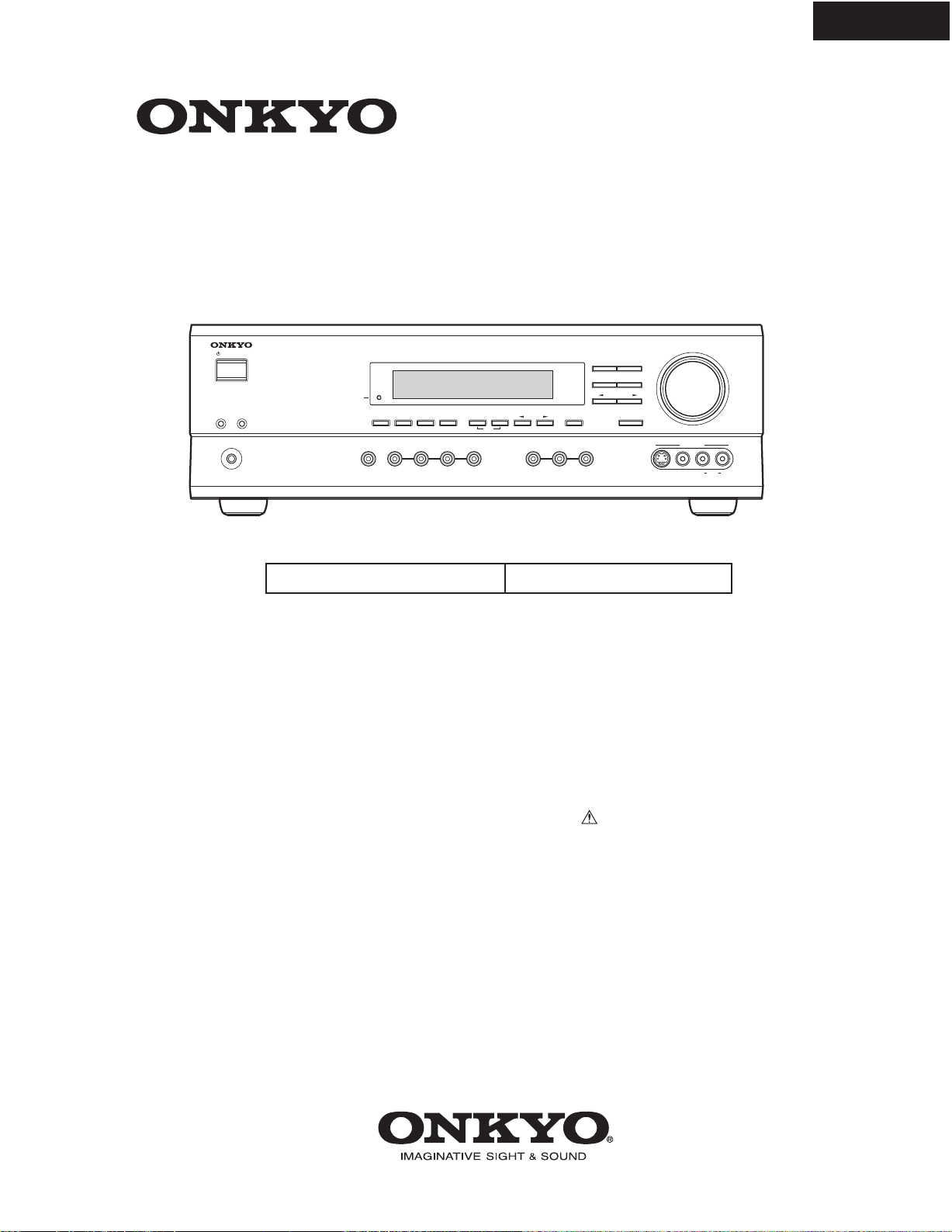
AV RECEIVER
HT-R510
Ref. No. 3778
062003
STANDBY/ON
AB
SPEAKERS
PHONES
BMDD
MODEL
STANDB
Y
DIMMER
DISPLA
Y
AUDIO
DVD
SELECTOR
HT-R510
SUBWOOFER
DIGITAL INPUT
VIDEO 1
VCR
MEMORY
MODE
VIDEO
2
3
VIDEO
Black models
SPEAKER ADJUST
TUNING
FM MODE
CLEAR
TAPE TUNER
120V AC, 60Hz
STEREO
DIRECT
DSP
SURROUND
PRESET/ADJUST
AUDIO ADJUST
C
D
MASTER VOLUME
INPUT
VIDEO 3
VIDEO L
S VIDEO AUDIO
R
SAFETY-RELATED COMPONENT
WARNING!!
COMPONENTS IDENTIFIED BY MARK ON THE
SCHEMATIC DIAGRAM AND IN THE PARTS LIST ARE
CRITICAL FOR RISK OF FIRE AND ELECTRIC SHOCK.
REPLACE THESE COMPONENTS WITH ONKYO
PARTS WHOSE PART NUMBERS APPEAR AS SHOWN
IN THIS MANUAL.
MAKE LEAKAGE-CURRENT OR RESISTANCE
MEASUREMENTS TO DETERMINE THAT EXPOSED
PARTS ARE ACCEPTABLY INSULATED FROM THE
SUPPLY CIRCUIT BEFORE RETURNING THE
APPLIANCE TO THE CUSTOMER.
Page 2
SERVICE PROCEDURES
1. Replacing the fuses
This symbol located near the fuses indicates that the
fuse used is fast operating type. For continued protection against
fire hazard, replace with same type fuse. For fuse rating refer to
the marking adjacent to the symbol.
Ce symbole indique que le fusible utlise est a rapide.
Pour une protection permanente, n'untiliser que fusibles de
meme type. Ce darnier est la qu le present symbol est
appse.
CIRCUIT NO. PART NO.
F6901,F6902 252198 or ! 8A-UL or
252261 ! 8A-T/UL-ST2,Fuse
F901 252198 or ! 8A-UL or
252261 !
2. To initialize the unit
This device employs a microprocessor to perform various
functions and operations. If interference generated by an external
power supply, radio wave, or other electrical source results in
accident which causes the specified operations and functions to
operate abnormally.
To perform a result, please follow the procedure below.
DESCRIPTION
8A-T/UL-ST2,Fuse
HT-R510
1.Press and hold down the VIDEO-1 button, then press the
STANDBY/ON button.
2.After "CLEAR" is displayed, the preset memory and each
mode stored in the memory, such as surround, are
initialized and will return to the factory setting.
3. Unplug the power supply cord.
3. Safety-check out
(U.S.A. model only)
After correcting the original service problem, perform the
following safety check before releasing the set to the customer.
Leakage Current Check
Measure leakage current to a known earth ground(water pipe,
conduit, etc.) by connecting a leakage current tester between
the earth ground and exposed metal parts of the appliance
(input/output terminals, screwheads,metal overlays, etc.).
Plug the power supply cord directly into a 120V AC 60 Hz outlet
and turn Standby switch on. Any current meausred must not
exceed 0.5mA.
Page 3
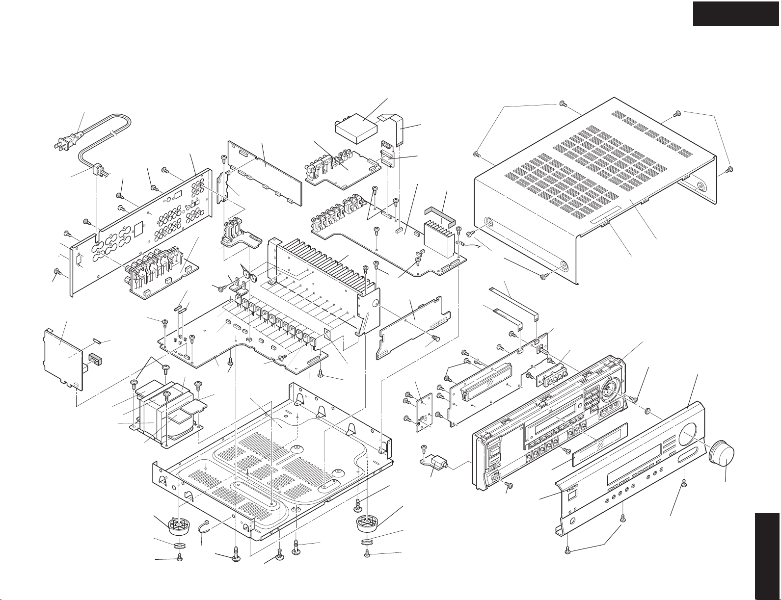
EXPLODED VIEW
HT-R510
33
11
U24
P901
U23
T901
33
F901
63
33
2
U31
P101
U9
31
U15
U14
U10
U27
U28
2
F6901
F6902
Q6050
Q6060
9
9
U21
U13
13
2
Q6055
5
U26
Q6065
55
2
12
U17
U1
54
2
2
U12
10
U4
P7503
2
17
17
P7502
U3
U6
17
16
18
1
2
51
U25
21
22
23
56
52
25
53
53
24
HT-R510
6
8
8
7
21
22
23
U5
2
Page 4
HT-R510
ID+
3
b
8
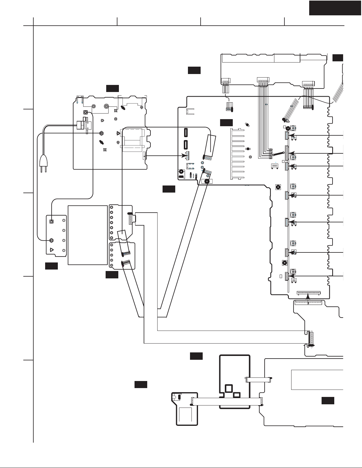
WIRING VIEW
1
2
7
P911A
3
NAPS-7844,
Transformer
terminal
PC board ass'y
4
P912A
U23
P913A
5
3
1
A
P926
E921
P911
P908
AC-G
AC-GAC-H
AC-H
P909
P901A
T901
POWER
TRANSFORMER
NPT-1465D
NAPS-7846,
Secondary
terminal
PC board ass'y
P902
P918
P912
P922
P921
NAETC-7835,Speaker
terminal PC board ass'y
NAPS-7845,Primary circuit
U24
PC board ass'y
P917
P913
P923
120V
P922A
S902
220V
P923A
T902
P925
P921A
P931A
NAETC-7834,
Secondary
PC board ass'y
JL9501B
141312111098
15 16 17 18 19
JL6952B
JL6951B
U25
BCD
U2
P6931A
U13
P6801
JL6803B
U14
JL6805B
P6802
JL6804B
P6800
NCETC-7835
P6906
P931
P6907
C6708
D6705
P6910
D6706
P995B
P997A
P6909
JL6952A
JL6951A
P996A
JL6805A
U21
NAAF-7842,
P6923
P6922
P995A
P6801
P6301
JL640
P6000
JL6804A
P6903
P6011A
COM
TH2
TH1
P6001
P6073A
P6002
P6802
JL6803A
2A
R6040
L
ID+
ID-
P6080
-B1
R6041
R
ID-ID+
P6081
R6042
ID+
ID-
P6082
Power amplifier
PC board ass'y
P6072
P6072A
P6003
P6004
P6005
R6043
P6083
ID-ID+
R6044
ID-
ID+
P6084
R6045
ID-
ID+
P6085
P6931
NAETC-78
circuit PC
JL9501
U4
NCSW-7404
NASW-7404,
Standby switch
PC board ass'y
U5
JL7501B
JL7501A
NAETC-7405,
5
Headphone
terminal PC
board ass'y
JL7502B
P7501
JL7502A
NADIS-7403,Display circui
U3
Page 5
HT-R510
WIRING VIEW
U28
1
2
3
NAETC-7849,
Thermal detector
PC board ass'y
JL6402B
P6000A
U9
P6011A
P6001A
P6002A
NAAF-7830,
Driver circuit
PC board ass'y
P6003A
P6004A
A
P306A
BCD
U6
V4Y
GND
V4C
GND
P302
P304P305
P301
P351
U17
P261B
V4
P253B
NAETC-7838,
Connector PC
board ass'y
P801B
P801
P7701
P7701
P206A
P243A
P206B
U283
P253A
U282
U1
NADG-7821,
DSP circuit
PC board ass'y
P306
P7502B
P412B
P261A
P101
NAETC-7406,
Front video
PC board ass'y
U26
NAVD-7847,Video
circuit PC board ass'y
P281
U281
P282
P243B
P241
P201
P242A
U10
NAVD-7831,Component
video PC board ass'y
P203
P202
P204
P6005A
U12
4
-7833,Const. voltage
C board ass'y
5
ircuit PC board ass'y
P7503B
GND
GND
HPL
HPE
HPR
+5.6V
FLAC
FLAC
P7503A
P410B
P7502A
P410A
P411B
P411A
P6403
TUNER
U31
PACK
: Flat cable
: Jumper Wire
: Socket
: PC board to PC board
Page 6
Controls & Connectors
Front Panel
1234789JLK5M6
HT-R510
STANDBY/ON
STANDBY
AB
SPEAKERS
PHONES
SELECTOR
AUDIO
DISPLAY
DIMMER
DVD
NPQSTRO
A
STANDBY/ON button
This button is used to set the HT-R510 to On or Standby. For
models with a POWER switch, this button has no effect unless
the POWER switch is set to ON.
B
STANDBY indicator
This indicator lights up when the HT-R510 is in Standby
mode, and it flashes while a signal is being received from the
remote controller.
DIMMER button
C
This button is used to adjust the display brightness.
D
DIGITAL INPUT button
This button is used to assign the digital inputs.
SUBWOOFER MODE button
E
This button is used to select the Subwoofer modes.
MEMORY button
F
This button is used when storing and deleting radio presets.
G
FM MODE button
This button is used to select the FM radio Stereo and Mono
modes. It’s also used when deleting radio presets.
TUNING [ ] [ ] buttons
H
These buttons are used to tune into radio stations.
I
Remote control sensor
This sensor receives control signals from the remote controller.
J
Listening mode buttons
These buttons are used to select the listening modes.
PRESET/ADJUST [ ] [ ] buttons
K
DIGITAL INPUT
VIDEO 1
VCR
SUBWOOFER
MODE
VIDEO
MASTER VOLUME
STEREO
DIRECT
DSP
SURROUND
PRESET/ADJUST
SPEAKER ADJUST
TUNING
FM MODE
MEMORY
CLEAR
2
3
VIDEO
M
TAPE TUNER
SPEAKER A & B buttons
C
AUDIO ADJUST
INPUT
D
VIDEO 3
VIDEO L R
S VIDEO AUDIO
These buttons are used to turn speaker sets A and B on and off.
N
PHONES jack
This 1/4-inch phone jack is for connecting a standard pair of
stereo headphones for private listening.
O DISPLAY button
This button is used to display various information about the
currently selected source.
P AUDIO SELECTOR button
This button is used to select the input signal format.
Q Input selector buttons
These buttons are used to select the audio and video sources:
CD, DVD, TAPE, TUNER, VIDEO 1, VIDEO 2, or VIDEO 3.
R SPEAKER ADJUST button
This button is used to adjust various speaker-related parameters.
S AUDIO ADJUST button
This button is used to set the Bass, Treble, Late Night, Cinema
Filter, Center Image, Panorama, Dimension, and Center Width
functions.
T VIDEO 3 INPUT connectors
These S-Video, composite video (RCA/phono), and analog
audio (RCA/phono) inputs can be used to connect a video
camera or games console.
This button is used to select radio presets and adjust parameter
values.
L
MASTER VOLUME control
This control is used to set the volume of the HT-R510.
Page 7

Controls & Connectors—Continued
Display
12 3 4
56
1 A & B speaker indicators
Indicator A lights up when speaker set A is on. Indicator B
lights up when speaker set B is on.
2 MUTING indicator
This indicator flashes when the HT-R510 is muted.
3 Source/listening mode indicators
These indicators display information about the currently
selected source and listening mode.
4 Tuning indicators
TUNED: This indicator lights up when the HT-R510 is
tuned into a radio station.
AUTO: This indicator lights up when the Auto Tuning
function is on.
MEMORY: This indicator lights up when programming
radio presets.
FM STEREO: This indicator lights up when the
HT-R510 is tuned into a stereo FM station.
5 SLEEP indicator
This indicator lights up when the Sleep function has been set.
6 Message area
This area of the display shows various information about the
currently selected source.
HT-R510
Page 8
Controls & Connectors—Continued
Rear Panel
HT-R510
16
COMPONENT VIDEO
VIDEO 1
/2/3
DVD IN
IN
DIGITAL INPUT
OPTICAL COAXIAL
IN
L
SUBWOOFER
PRE OUT
R
CD
789JK M N
A COMPONENT VIDEO
These RCA/phono connectors can be used to connect a TV,
DVD player, or other AV component with component video
inputs and outputs.
B AM ANTENNA
These push terminals are for connecting an AM antenna.
C FM ANTENNA
This connector is for connecting an FM antenna.
D FRONT SPEAKERS B
These push terminals are for connecting speaker set B.
E FRONT SPEAKERS A, SURROUND SPEAKERS,
CENTER SPEAKER & SURROUND BACK
SPEAKER
These terminal posts are for connecting speaker set A, including the front, surround, center, and surround-back speakers.
They accept bare wires or banana plugs.
F AC OUTLET
This switched AC outlet can be used to supply power to
another AV component.
G DIGITAL INPUT OPTICAL 1, 2 & COAXIAL
ANTENNA
OUT
12
OUT
TAPE
AM
Y
B
P
PR
REMOTE
CONTROL
IN
L
R
VIDEO 2
IN
IN
VIDEO 2
OUT
OUT
FM
75
VIDEO 1
VIDEO 1
IN
IN
DVD MONITOR
OUT
IN
SURR
FRONT
L
R
DVD
CENTER
SUB
WOOFER
VIDEO
S VIDEO
L
4532
L
R
SURROUND
SPEAKERS
FRONT
SPEAKERS B
L
R
FRONT
SPEAKERS A
L
R
HT-R510
K
This (Remote Interactive) connector can be connected to
the connector on another Onkyo AV component, for
example, a CD player, DVD player, or cassette recorder. The
HT-R510’s remote controller can then be used to control that
component. To use , you must make an analog RCA/
phono connection between your HT-R510 and the other AV
component, even if they are connected digitally.
L VIDEO 1 IN/OUT & VIDEO 2 IN
These connectors can be used to connect a VCR or other AV
component. There are RCA/phono connectors for connecting
to stereo analog audio inputs and outputs, and S-Video and
composite video (RCA/phono) connectors for connecting to
video inputs and outputs.
M DVD IN/MULTI CH INPUT
The FRONT, SURR, CENTER, and SUBWOOFER RCA/
phono connectors can be used to connect AV components with
multiple analog audio outputs, including DVD players with
individual 5.1 surround analog outputs. There’s an S-Video
input and composite video (RCA/phono) input for connecting
the video signal.
N MONITOR OUT
These S-Video and composite video (RCA/phono) outputs can
be connected to the video input on your TV or projector.
CENTER
SPEAKER
SURROUND BACK
SPEAKER
AC OUTLET
AC 120 V 60 Hz
SWITCHED
W 1 A
120
MAX.
These optical and coaxial connectors can be used to connect a
CD, DVD, or LD (laser disc) player, or other AV component
with digital outputs.
H SUBWOOFER PRE OUT
This RCA/phono connector can be used to connect an active
subwoofer.
I CD IN
These RCA/phono connectors can be used to connect a CD
player with analog outputs.
J TAPE IN/OUT
These RCA/phono connectors can be used to connect a cassette recorder, MiniDisc recorder, or other recorder with analog inputs and outputs.
Tip:
A turntable with a built-in preamp can be connected to a pair of
unused HT -R510 analog inputs. To connect a turntable without
a built-in preamp, you’ll need a commercially av ailable phono
preamp.
Page 9

Specifications
HT-R510
AMPLIFIER SECTION
Continuous Average Power output (FTC)
All channels: 100 watts per channel min. RMS at
Dynamic power output:
Total Harmonic Distortion: 0.08% at rated power
IM Distortion: 0.08% at rated power
Damping Factor: 60 at 8 Ω
Input Sensitivity and Impedance
DIGITAL INPUT (OPTICAL 1, 2): 0.5 Vp-p, 75 Ω
DIGITAL INPUT (COAXIAL): 0.5 Vp-p, 75 Ω
LINE (CD, VIDEO 1, 2, 3, TAPE): 200 mV, 47 kΩ
Multichannel Input
(DVD FRONT L/C/R, SURR L/R): 200 mV, 47 kΩ
(SUBWOOFER): 36 mV, 47 kΩ
Output Level and Impedance
Rec out (TAPE, VIDEO 1): 200 mV, 470 Ω
Pre out (SUBWOOFER): 1 V, 470 Ω
Frequency Response: 10 Hz to 100 kHz,
Tone Control
Bass: ±12 dB at 20 Hz
Treble: ±12 dB at 20 kHz
Signal-to-Noise Ratio: CD/TAPE: 100 dB
Muting: –50 dB
8 Ω, 2 channels driven from 20 Hz
to 20 kHz with no more than 0.08%
total harmonic distortion.
230 watts
170 watts
115 watts
0.08% at 1 watt output
0.08% at 1 watt output
+1/–3 dB (Direct mode)
(IHF-A, Direct mode)
× 2 at 3 Ω
× 2 at 4 Ω
× 2 at 8 Ω
VIDEO SECTION
Input Sensitivity and Impedance
VIDEO (DVD, VIDEO 1, 2, 3): 1 Vp-p, 75 Ω
S VIDEO (DVD, VIDEO 1, 2, 3): 1 Vp-p, 75 Ω (Y)
COMPONENT VIDEO 1, 2: 1 Vp-p, 75 Ω (Y)
Output Level and Impedance
VIDEO (VIDEO 1, 2, MONITOR): 1 Vp-p, 75 Ω
S VIDEO (VIDEO 1, 2, MONITOR): 1 Vp-p, 75 Ω (Y)
COMPONENT VIDEO OUT: 1 Vp-p, 75 Ω (Y)
0.28 Vp-p, 75 Ω (C)
0.7 Vp-p, 75 Ω (P
0.28 Vp-p, 75 Ω (C)
0.7 Vp-p, 75 Ω (P
B
B
, PR)
, PR)
TUNER SECTION
FM
Tuning Range: 87.50-108.00 MHz (100 kHz steps)
Usable Sensitivity
Mono: 11.2 dBf, 1.0 µV (75 Ω, IHF)
Stereo: 17.2 dBf, 2.0 µV (75 Ω, IHF)
50 dB Quieting Sensitivity
Mono: 17.2 dBf, 2.0 µV (75 Ω)
Stereo: 37.2 dBf, 20.0 µV (75 Ω)
Capture Ratio: 2.0 dB
Image Rejection Ratio: 40 dB
IF Rejection Ratio: 90 dB
Signal-to-Noise Ratio
Mono: 76 dB
Stereo: 70 dB
Alternate Channel Attenuation: 55 dB
Selectivity: 50 dB (DIN)
AM Suppression Ratio: 50 dB
Total Harmonic Distortion
Mono: 0.2%
Stereo: 0.3%
Frequency Response: 30 Hz-15 kHz, –1.0 dB
Stereo Separation: 45 dB at 1 kHz
0.9 µV (75 Ω, DIN)
23 µV (75 Ω DIN)
30 dB at 100 Hz-10 kHz
AM
Tuning Range: 530-1,710 kHz (10 kHz steps)
Usable Sensitivity: 30 µV
Image Rejection Ratio: 40 dB
IF Rejection Ratio: 40 dB
Signal-to-Noise Ratio: 40 dB
Total Harmonic Distortion: 0.7%
GENERAL
Power Supply and Power Consumption:
AC 120 V, 60 Hz 5.2 A
Dimensions (W
Weight: 21.8 lbs., 9.9 kg
× H × D): 17-1/8" × 5-7/8" × 14-13/16"
× 150 × 376 mm
435
REMOTE CONTROL
Transmitter: Infrared
Signal range: Approx. 16 ft., 5 meters
Power supply:
Specifications and features are subject to change without notice. Power supply and voltage vary depending on the area in which the unit is purchased.
Two “AA” batteries (1.5 V
× 2)
Page 10
Controls & Connectors—Continued
HT-R510
Remote Controller—RCVR Mode
RC-518M
1J
2
3
4
K
L
Press this to select
RCVR mode
5
M
N
O
6
7
8
9
P
This page describes only those buttons that can be used to
control the HT -R510 when the remote controller is in RCVR
mode (Receiver mode).
To select RCVR mode, press the [RCVR] button.
A SLEEP button
This button is used to set the Sleep function. This function can
be set only with the remote controller.
B STANDBY/ON button
This button is used to set the HT-R510 to On or Standby.
C Listening mode buttons
These buttons are used to select the listening modes.
D CINE FLTR button
This button is used to set the Cinema Filter function.
E LATE NIGHT button
This button is used to set the Late Night function.
F TEST, CH SEL & LEVEL [ ] [ ] buttons
These buttons are used to set the level of each speaker individually. This function can be set only with the remote controller.
G AUDIO SEL button
This button is used to select analog or digital inputs for the
CD, DVD, TAPE, VIDEO 1, VIDEO 2, and VIDEO 3 sources.
H Input selector buttons
These buttons are used to select the audio and video sources:
CD, DVD, TAPE, TUNER, VIDEO 1, VIDEO 2, and
VIDEO 3.
I MUTING button
This button is used to mute the HT-R510. This function can be
set only with the remote controller.
J PRESET [ ] [ ] buttons
These buttons are used to select radio presets.
K DIMMER button
This button is used to adjust the display brightness.
L Remote Controller Mode buttons
These buttons are used to select the remote controller modes.
To select RCVR mode, press the [RCVR] button.
M SP A & SP B buttons
These buttons are used to turn on and off speaker sets A and B
individually.
N AUDIO ADJUST button
This button is used to set the Bass, Treble, Late Night, Cinema
Filter, Center Image, Panorama, Dimension, and Center Width
functions.
O ADJUST [ ] [ ] buttons
These buttons are used to adjust the functions selected with
the AUDIO ADJUST button.
P VOLUME [ ] [ ] buttons
These buttons are used to set the volume of the HT-R510.
Page 11
Precautions—
1.
Recording Copyright
Continued
—Unless it’s for personal use only,
recording copyrighted material is illegal without the permission
of the copyright holder.
2.
AC Fuse
—The A C fuse inside the HT-R510 is not user-serviceable. If you cannot turn on the HT-R510, contact your Onkyo
dealer.
3.
Care
—Occasionally you should dust the HT -R510 all over with
a soft cloth. For stubborn stains, use a soft cloth dampened with
a weak solution of mild detergent and water. Dry the HT-R510
immediately afterwards with a clean cloth. Don’t use abrasive
cloths, thinners, alcohol, or other chemical solvents, because
they may damage the finish or remove the panel lettering.
4.
Power
WARNING
BEFORE PLUGGING IN THE UNIT FOR THE FIRST TIME,
READ THE FOLLOWING SECTION CAREFULLY.
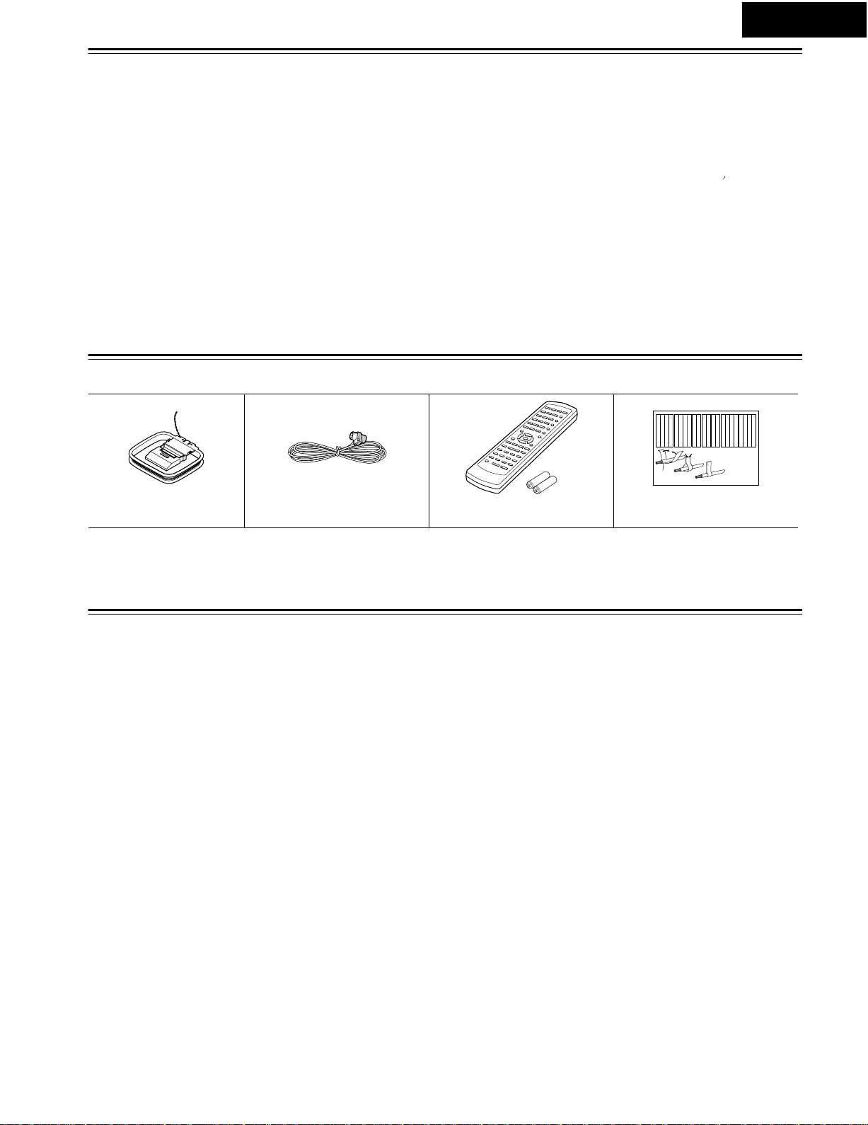
Supplied Accessories
Make sure you have the following accessories:
HT-R510
AC outlet voltages vary from country to country . Make sure that the
voltage in your area meets the voltage requirements printed on the
HT-R510’s rear panel (AC 120 V, 60 Hz).
Setting the [STANDBY/ON] switch to STANDBY does not fully
shutdown the HT -R510. If you do not intend to use the HT-R510 for
an extended period, remove the power cord from the AC outlet.
Memory backup
The HT -R510 uses a battery-less memory backup system in order to
retain radio presets and other settings when it’s unplugged or in the
case of a power failure. Although no batteries are required, the
HT-R510 must be plugged into an AC outlet in order to charge the
backup system.
Once it has been charged, the HT-R510 will retain the settings for several weeks, although this depends on the environment and will be shorter in humid climates.
Left
Left
Left
Left
Left
Left
Right
Right
Surround
Surround
Surround
Surround
Right
Left
Surround
Right
Surround
Left
3
Right
Right
Right
Right
Center
Center
Zone 2
Zone 2
Zone 2
Zone 2
Surround Back
Surround Back
Surround Back
Surround Back
Zone 2
Right
Zone 2
Left
Center
Zone 2
Right
Zone 2
Left
Surround Back
Right
Surround Back
Left
Center
Surround Back
Right
Surround Back
Left
AM loop antenna Indoor FM antenna
Remote controller &
two batteries (AA/R6)
Left
Left
Left
Left
Front
Front
Front
Front
Right
Right
Right
Right
Zone 2
Zone 2
Zone 2
Zone 2
/
/
/
/
Surround
SP-B
SP-B
SP-B
SP-B
Zone 2
Zone 2
Zone 2
Zone 2
/
/
/
/
Front
Left
Front
Right
SP-B
Left
SP-B
Right
Surround
Front
Left
Front
Right
SP-B
Left
SP-B
Right
1
2
Speaker Cable
Speaker cable labels
* In catalogs and on packaging, the letter added to the end of the product name indicates the color of the HT-R510. Specifications and operation are the same
regardless of color.
Features
Amp
• 6-channel amplifier
• 100 watts per channel min. RMS at 8 Ω, 2 channels driven
from 20 Hz to 20 kHz with no more than 0.08% total harmonic distortion
• WRAT (Wide Range Amplifier Technology)
• Optimum gain volume circuitry
Audio/Video
• Dolby*1 Digital EX and Dolby Pro Logic II
• DTS, DTS-ES Matrix/Discrete 6.1, and DTS Neo:6 pro-
*2
cessing
• Cinema Filter function
• Advanced 24-bit DSP chip (5 DSP soundfields)
• Linear PCM 96 kHz/24-bit D/A converters on all channels
• Adjustable crossover (60, 80, 100, 120, 150 Hz)
•2 component video inputs, 1 output
•4 S-Video inputs, 2 outputs
•3 assignable digital inputs (2 optical, 1 coaxial)
• Subwoofer pre out
• Color-coded multi-channel inputs
• Color-coded speaker terminal posts (SPEAKERS B use
push-type terminals)
FM/AM T uner
• 30 FM/AM presets
• FM auto tuning
*1. Manufactured under license from Dolby Laboratories. “Dolby”, “Pro Logic” and the double-D symbol are trademarks of Dolby Laboratories.
*2. “DTS,” “DTS-ES Extended Surround,” and “Neo:6” are trademarks of Digital Theater Systems, Inc.
Page 12
HT-R510
A
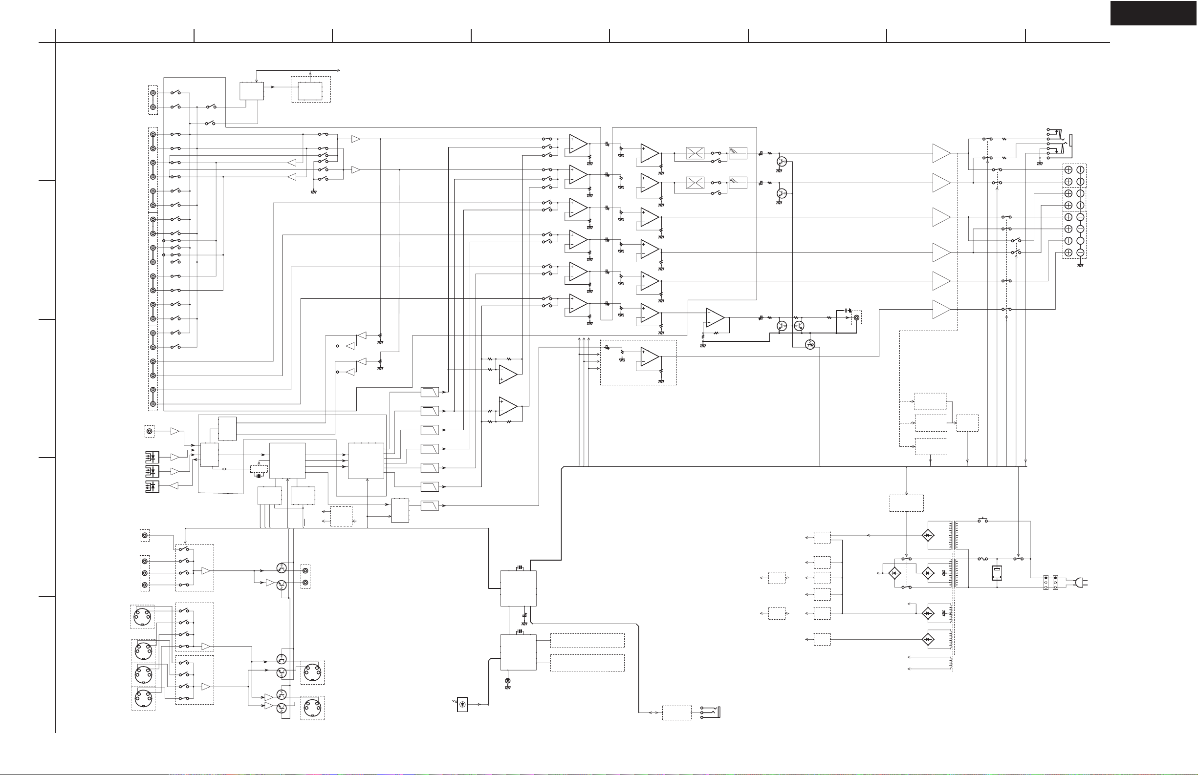
BLOCK DIAGRAM
VIDEO3
1
CD
TAPE OUT
TAPE IN
VIDEO3
2
3
4
5
VIDEO-2 IN
VIDEO-1 OUT
VIDEO-1 IN
DVD
MLS/MRS
C/SW
COAXIAL
OPTICAL 1
OPTICAL 2
OPTICAL OUT
COMPOSITE VIDEO INPUT
VIDEO3
VIDEO2
VIDEO1
DVD
VIDEO 3
C
S-VIDEO INPUT
DVD
C
C
C
VIDEO 2
VIDEO 1
BCDEFGH
BD3811K1
80
79
2
1
72
71
4
3
6
5
73
8
74
7
76
75
S
10
9
12
S
11
14
13
16
15
AK4586
DIR
CTLA/B
LA7956
6dB
VIDEO SW
Y
Y
Y
LA7956
6dB
LA7956
6dB
Y
78
77
(1/2)
AK4586
2CH A/D
96/24
FM/AM
TUNER
PACK
OSC
12.288MHZ
FLASH
ROM
A17
A16
A15
0dB
0dB
0dB
RDS
DECODER
BU1923F
MPP MODEL ONLY
1
1
CS493292
DSP
1M SRAM
(MJJ ONLY)
RST.CS.INTREQ/CL/DA/SCDO
ROM/RAM
VMUT1
VMUT2
COMPOSITE VIDEO OUT
MONITOR OUT
VIDEO 1
S-VIDEO OUTPUT
Y
C
Y
C
1
1
1
18
-1
NC
1
20
-1
NC
17
19
AK4586
96/24
6CH D/A
AK4586
+2.5V
DSP
+5V
+3.3V
MEMORY
MONITOR OUT
VIDEO 1
-6dB
INPUT ATT
SL
SR
SW
SB
2CH D/A
RST.CS/CL/DA/CDTO/INT1.2.
AK4384
L
R
C
50KLPF
50KLPF
50KLPF
50KLPF
50KLPF
50KLPF
50KLPF
2321262528
REMOTE
SENSOR
27
OPAMP
10.5dB
OPAMP
12.5MHZ
MAIN
MICROPROCESSOR
78K/4
5MHZ
SUB MICRO
PROCESSOR
78K/0
STANDBY
UPD780232GC-8BT
INPUT GAIN
24
22
UPD784225AGC
BACK UP
INPUT GAIN
0/6dB
INPUT GAIN
0/6dB
INPUT GAIN
0/6dB
INPUT GAIN
0/6dB
INPUT GAIN
0/6dB
INPUT GAIN
0/6dB
SELDA
KEY
FL DISPLAY
69
66
43
40
30 31
33
SELMUT
SELCL
MASTER
VOLUME
0~103dB
68
65
42
39
34
BD3812
OUTPUT GAIN
0~18dB
OPAMP
OUTPUT
GAIN
0~18dB
OPAMP
OUTPUT GAIN
0~18dB
OPAMP
OUTPUT GAIN
OPAMP
0~18dB
OUTPUT GAIN
0~18dB
OPAMP
OUTPUT GAIN
0~18dB
OPAMP
OUTPUT
GAIN
OPAMP
RI
INTERFACE
BASS/TREBLE
BASS/TREBLE
36
15dB
OPAMP
BASSBOOST
55
57
38
37
35
Q305
AUDIO
AUDIO
RI
STANDBY
+7V
AF/TU
-7V
DSP/TU
-VP
+12V
VIDEO
-12V
-12V
AMUT
+5.6V
-27V
+12V
+12V
AF
+5V
SWPO
SEC1H RELAY
+B1H
+B1
Power Amplifier
VOLTAGE
SENSOR
CURRENT
SENSOR
VOLTAGE
SENSOR
SEC1H
SEC1H
CONTROL
+B1L
RELAY
+B2
FLAC
FL TUBE
FLAC
+27dB
VOLH
SEC1
SEC2
SEC3
+27dB
+27dB
+27dB
+27dB
+27dB
T902
T901
PROTE
CTION
PRO
PRI
SPHP
SPF
SPCS
HPMUT
POWER SW
POWER
RELAY
FUSE
SPB
HPDET
POWER
AC OUTLET
HEADPHONE
L
R
SPBL
SPBR
SL
SR
C
SB
AC IN
Page 13
HT-R510
0
1SS352
C7502
L7504
A
BCD
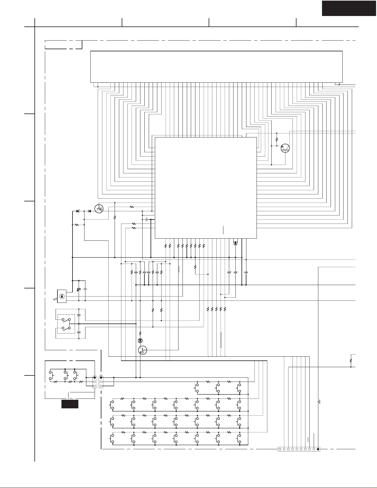
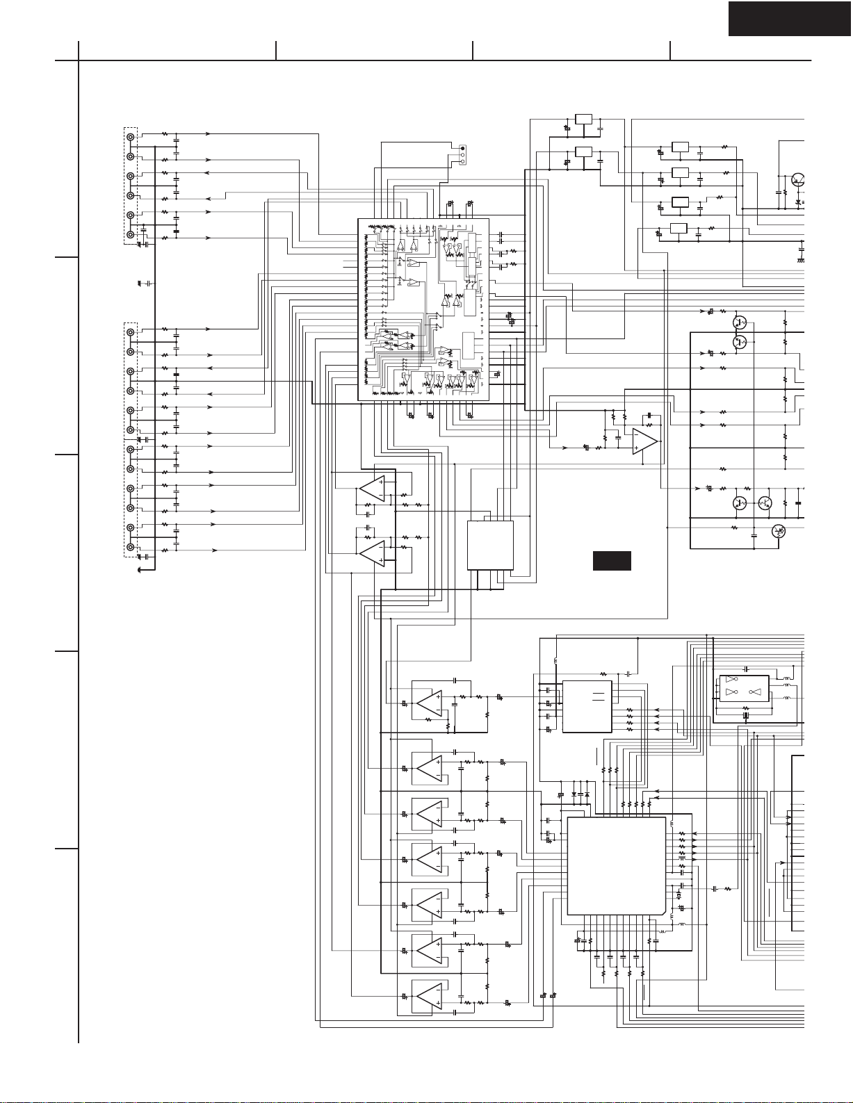
SCHEMATIC DIAGRAM 1-1 Display and video sections
NADIS-7403
Q7501 HNA-16MM39T
1
2
D7502
UDZ5.1B
R7505
220K
3
F2F2NPNPP35
59
Q7504
KRA103S
D7503
1SS352
P34
P33
P32
P31
P30
P29
P28
P27
P26
P25
P24
P23
P22
P21
P20
P19
P18
P17
P16
P15
P14
P13
P12
P11
P10P9P8P7P6P5P4P3P2P116G
30
31
32
33
34
35
36
37
38
39
40
41
42
43
44
45
46
47
48
49
50
51
52
53
54
55
56
57
58
41
42
43
P46/FIP3840
R7504
10K
R7532
SYSOUT
47K
R7506
4.7K
R7507
4.7K
C7507
104Z
22
21
P47/FIP3939
P50/FIP4038
P51/FIP4137
P52/FIP4236
P53/FIP4335
P54/FIP4434
P55/FIP4533
P56/FIP4632
P57/FIP4731
P60/FIP4830
P61/FIP4929
P62/FIP5028
P63/FIP5127
P64/FIP5226
VDD025
AVDD24
VSS023
ANI220
4.7K
R7508
22:ANI0
21:ANI1
ANI319
AVSS18
4.7K
R7509
P37/FIP3147
P40/FIP3246
P41/FIP3345
P42/FIP3444
41:P45/FIP37
42:P44/FIP36
43:P43/FIP35
P01/INTP116
P02/TI17
P20/SCK314
POO/INTP015
1K
1K
10K
10K
R7512
R7511
R7510
R7513
P36/FIP3048
UPD780232GC
-030-8BT
P21/SO313
10K
10K
R7514
R7515
P34/FIP2850
P35/FIP2949
Q7502
P2212
P2311
10K
R7516
P31/FIP2553
P32/FIP2652
P33/FIP2751
P24/BUSY10
P25SO19
P26/SI18
28
29
FIP23 55
61:FIP19
P27/SCK17 P30/FIP2454
RESET
6
26
27
FIP21 57
FIP22 56
IC5
X2
4
22
23
24
25
60
VLOAD
61
VDD259
FIP20 58
FIP18 62
FIP17 63
FIP16 64
FIP15 65
FIP14 66
FIP13 67
FIP12 68
FIP11 69
FIP10 70
FIP9 71
FIP8 72
FIP7 73
FIP6 74
FIP5 75
FIP4 76
FIP3 77
FIP2 78
FIP1 79
FIP0
80
VSS12
X13
1
VDD1
X7501
CST5.00MGW
15G
14G
13G
12G
11G
10G9G8G7G6G5G4G3G2G1GNPNPF1
10
11
12
13
14
15
16
17
18
19
20
21
10K
R7503
F1
123456789
2SC2712
Q7503
KTC3875
100K
2.7K
102J
2.7K
R7521
C7510 102J
C7509
220
R7531
D7505
STANDBY
Q7506
RN1402
KRC102S
S7625
VIDEO3
S7635
NG<
S7645
PRE
SET>
102J
C7511
R7522
10K
R7527
MEMO
PRE
2.7K
R7523
10K
R7526
K2
VIDEO2
RY
SET<
K3
S7624
S7634
S7644
102J
100/6.3
U7501
C7514
SPS4441E1
102J
C7517
104Z
C7516
4
S7501
104Z
C7515
SYSIN
S7615
SP B
R7614
820
S7614
STANDBY
R7613
560
JL7501B
JL7501A
S7616
SP A
R7615
1.2K
NASW-7404
U4
5
S7627
S7637
S7647
2.7K
R7520
C7508
K0
K1
GND
KEY0
2.2K R7621 330R7625 1.2K R7624820 R7623560 R7622470
R7626
S7626
FM
MODE
S7636
TUNI
NG<
S7646
ADJUST
TUNI
R7646 2.2K
AUDIO
IRF
STBYLED
VIDEO1
TAPE
DSP
S7643
R7518
VAJ
R7612
S7613
S7623
S7633
1K
560
VBJ
R7517
R7528
SBMDI
SBMLDY
470 R7611330
S7612
DIM
MER
DVD
S7622
S7632
TUNER
S7642
SURRO
UND
1K
1K
R7529 560
R7524
R7530
SBMDO
SBMCLK
SBMRST
SW
SEL
AUDIO
R7631
CD
R7641 330R7645 1.2K R7644 820 R7643 560 R7642 470
STE
102J
101J
C7522
MODE
330R7632 470R7633 560R7634 820R7635 1.2KR7636 2.2K
REO
C7523
S7611
S7621
S7631
S7641
C7513
INPUT
DIGITAL
DIS
PLAY
SP
DIRECT
104Z
K0K1K2
ADJUST
K3
SYSIN
HPDET
SBMDI
SBMDO
SBMLDY
TO NADG-7401
L7505
-VP
SBMCLK
SBMRST
220K
NCH1477
P7502A
100K
R7519
P75
D7507
Page 14
HT-R510
R7519
A
BCD
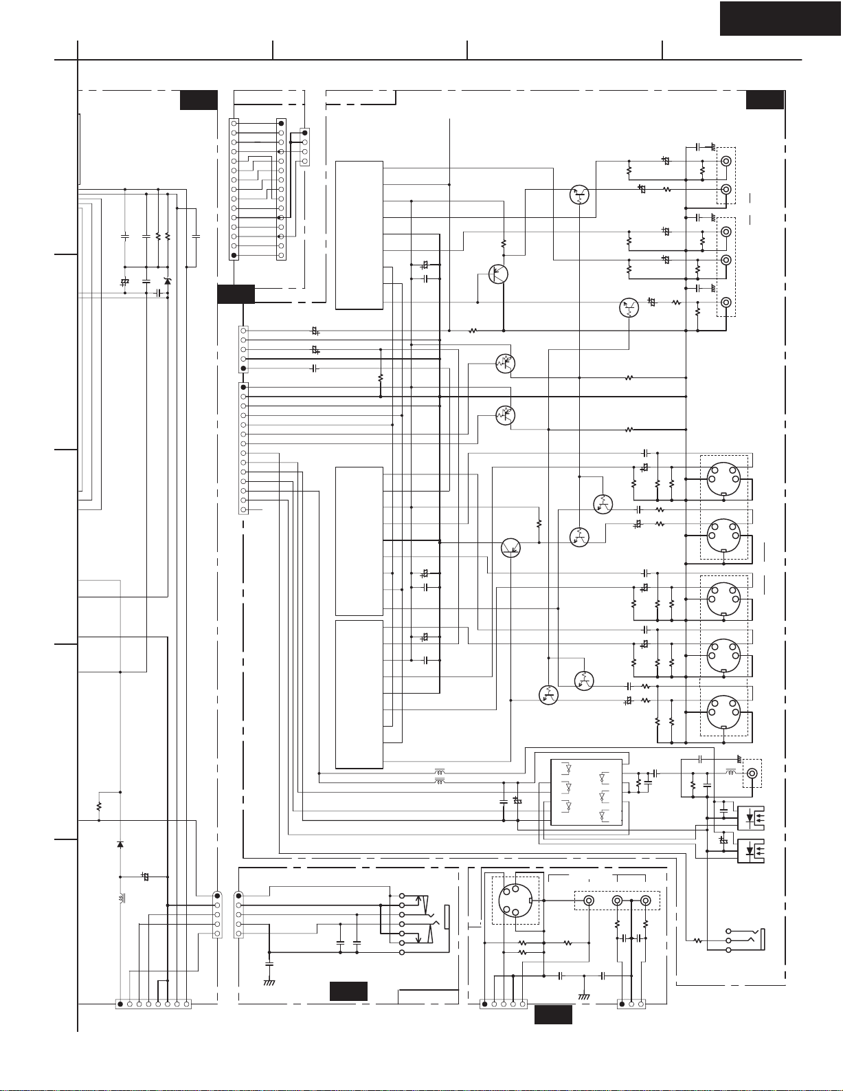
SCHEMATIC DIAGRAM 1-2 Display and video sections
U3
1
104Z
104Z
C7501
C7502
33/50
2
R7501
C7503
473Z
C7504
C7505
R7502
220
220
UDZ8.2B
D7501
473Z
NAETC-7838
RI
A
B
VMUT2
VMUT1
OPT2
DGND
TO NADG-7821
OPT1
+5V
COAX
104Z
C7506
OPTOUT
P801B
U17
P253A
P206B
OPTOUT
+12V
GND
GND
CNPT
V4
V4Y
V4C
+12V
GND
A
B
VMUT2
VMUT1
RI
OPT2
DGND
OPT1
+5V
COAX
P206A
3
4
100K
D7507
1SS352
C7521
220/6.3
HPDET
L7504
220K
NCH1477
5
+5.6S
P7503A
GND
HPL
HPR
HPE
GND
TO NAETC-7410
FAC2
FAC1
JL7502A
GND
HPL
HPE
HPR
JL7502B
E7501
C7518
102J
NAVD-7847
P243A
TO NAVD-7831
TO NAVD-7847
2.2/50
C217
C218
2.2/50
223Z
C219
C7519
102J
9
VIN4
VIN3
8
VCC
7
LA7956
VIN2
6
GND
5
VIN1
4
Q203
B
3
A
2
VIDEO OUT
1
R229
680K
VIN4
9
VIN3
8
VCC
7
LA7956
VIN2
6
GND
5
VIN1
4
Q212
B
3
A
2
VIDEO OUT
1
VIN4
9
8
VIN3
7
VCC
LA7956
6
VIN2
5
GND
4
VIN1
Q213
3
B
2
A
VIDEO OUT
1
C7520
102J
U5
C221
47/16
C222
223Z
C223
47/16
C224
223Z
C225
47/16
C226
223Z
L282
NCH-1452
L281
NCH-1452
P7501
HEADPHONE
NAETC-7405
R210
R230
680K
Q206
DTA114ES
KRA102M
KTA1267-GR
220K
220K
C286
223Z
C285
NAETC-7406
P253B
220
Q204
2SA933-S
KTA1267-GR
DTA114ES
KRA102M
Q205
Q209
2SA933-S
220
R228
Q209
Q211
RN1241
1
2
3
4
5
6
7 8
47/6.3
S
YC
R253
P251
R252 75R251 75
75
C253
104Z
P254
U6
Q201
RN1241
R208
680K
R209
680K
Q202
RN1241
C206
C207
Q207
RN1241
Q208
C208
C209
C212
C213
RN1241
Q210
223Z
Q281
74HCU04
VIDEO3 IN
V
R261
C263
104Z
P261B
680K
R207
470/16
R223
100K
R224
100K
223Z
2.2/50
C210
223Z
RN1241
223Z
2.2/50
223Z
2.2/50
R227
C214
C215
470/16
14
13
12
11
10
9
330
101J
C201
C203
C202
2.2/50
C204
2.2/50
C205
470/16
R225
680K
R219
R220 75
C211
470/16
680K
R226
680K
R221
R222
C283
R284
RL
C261
C262
2.2/50
R205
75
R212
75
R214
R218
223Z
C284
10K
R262
101J
75
C220
223Z
R202
R203
C216
223Z
R206
75
75R217
R211
75
75
R213
75
R216
75
75
100K
080D
330
C227
223Z
75
R201
75
75
100K
R204
YC
YC
75
R215
Y C
100K
C281
L283
223Z
022M
75
R281
C282
C287
223Z
R282
470
C288
47/6.3
U26
VIDEO-2
IN
P201
OUT
VIDEO-1
IN
P202
DVD IN
MONITOR
OUT
VIDEO-2
IN
P201
CY
OUT
VIDEO-1
IN
P202
CY
DVD IN
MONITOR
101J
U281
U282
P282
P281
Page 15
HT-R510
G
-
7
6
0
R
0
K
K
K
222J
5
3
Z
K
K
J
J
8
G
A
BCD
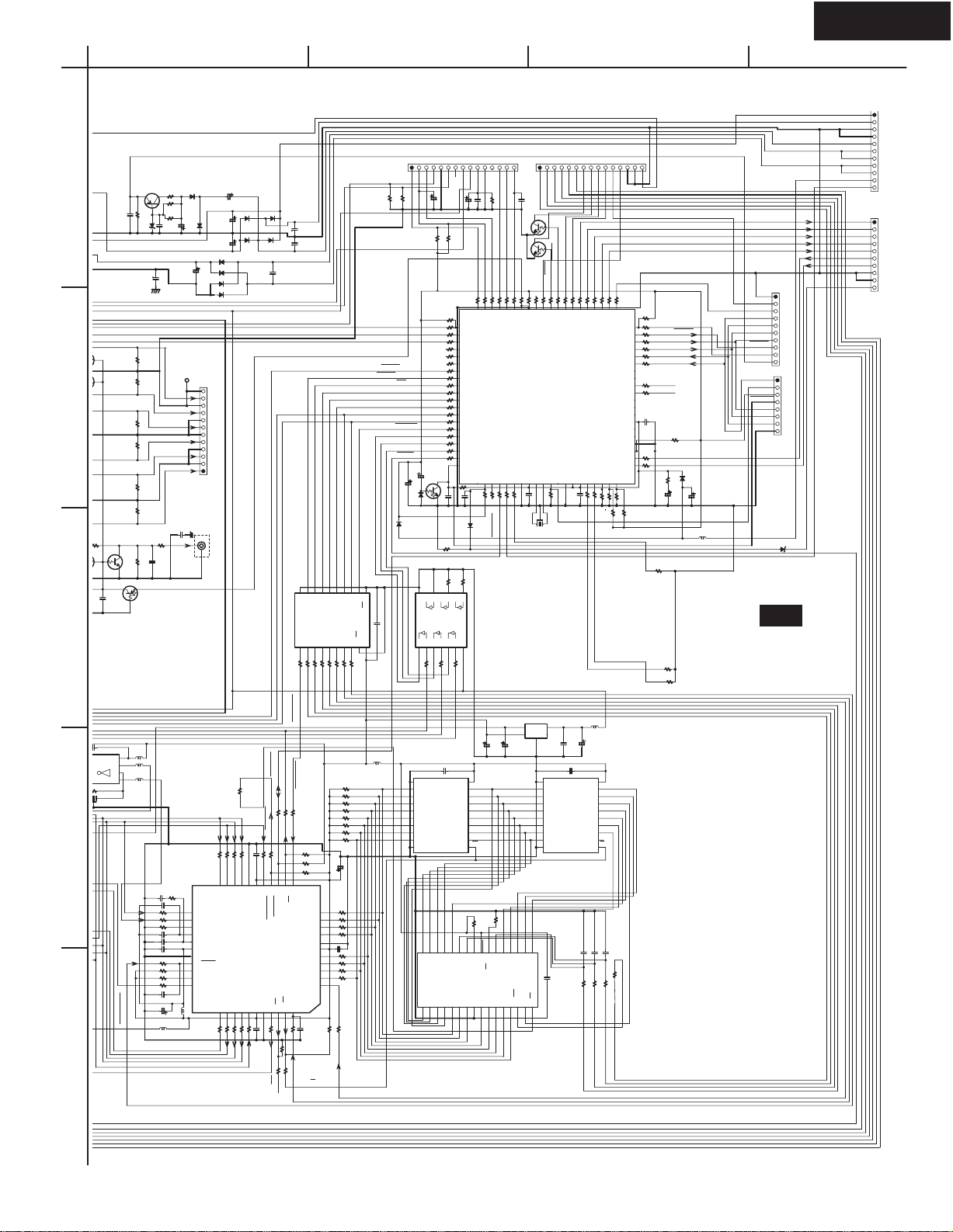
SCHEMATIC DIAGRAM 2-1 Digital and main microprocessor sections
78L07
Q321
1
2
3
CD
TAPE-1 OUT
TAPE-1 IN
VIDEO-2 IN
IDEO-1 OUT
VIDEO-1 IN
DVD
MLS/MRS
C/SW
P301
P304
P305
C322
104Z
C323
104Z
C325
104Z
C326
104Z
C308
R300
103Z
330
330
330
330
R310
330
330
R311
R312
330
330
R313
R314
330
330
R315
R316
330
330
R317
R318
330
R319
R320
330
330
R301
R302
R303
R304
R305
330
330
330
R321
+7V
CDR
101K
CDL
C301 C300C321 C320 C319 C318 C317 C316 C315 C314 C313
101K
TOR -12VAF
101J
C302
101J
TOL
C303
TIR
C305 C304
C311 C310
C312
101J
101J
101J
101J
101J
101J
101J
101J
101J 101J
101J
101J
101J
101J
TIL
V2IR
V2IL
V1OR
V1OL
V1IR
V1IL
DVDR
DVDL
MSW
MC
47k
CDR
1
47k
CDL
2
47k
TIR
3
47k
TIL
4
47k
V3IR
5
47k
V3IL
6
47k
V2IR
7
47k
V2IL
8
47k
V1IR
9
47k
V1IL
10
47k
DVDR
11
47k
DVDL
12
47k
MRS
13
47k
MLS
14
47k
MSW
15
47k
MC
16
47k
ADCL
17
18
ADCR SELDA
19
20
47k
DAC_R
21
47k
DMIXR
22
47k
DAC_L
23
47k
DMIXL
24
47k
NJM4565M
OR MPC4570
7
Q302
R36110K
C327
330J
C328
R362
10K
Q302
1
NJM4565M
4
OR MPC4570G2
V4R
80
47k
DAC_RS
8
330J
V4L
TUL
78
79
47k
47k
272625
DAC_LS
DAC_SW
5
6
2
3
TUR
77
47k
47k
28
DAC_C
DAC_R
V1OL
V1OR
47k
297032
30
C334
10/16
DAC_L
R347
10K
R387
2.2K
R386
2.2K
R348
10K
TUL
TUR
470
31
R359
470
R360
TOL
C333
10/16
DAC_SW
TOR
71
7273747576
BD3811K1
33
34
Q301
35
OUT_C
C329
10/16
69
68
363738
OUT_LS
OUT_SW
P261A
C330
10/16
67
66
65
64
63
62
TREBLE
61
60
59
58
57
56
55
54
53
BAAS
BOOST BASS
52
VCC
51
50
VEE
49
MUT
48
CL
47
DA
LOGIC
46
45
44
43
42
41
40
39
C332
10/16
OUT_RS
OUT_SW
OUT_C
OUT114
OUT213
Q323BD3812F
AGND12
IN1
1
C335
332J
C336
332J
R363
C338
10K
563J
R364
C340
10K
563J
C347
100/16
C348
100/16
SELCK
C331
10/16
CL 8
DA 9
SEL 12
MUTE10
DGND11
IN23
AGND24
AGND36
VCC7
VEE5
+7V
-7V
OUT_L
OUT_R
C359
10/16
-7V
C362
C366
104Z
O
I
G
10/16
Q322
G
SELMUT
C349
10/16
79L07
IO
C367
47K
R368
R367
1K
104Z
R369
C350
2.2K
R370
6
221J
Q305
5
NJM4565M
OR MPC4570
5.6K
+12VAF
C6404
10/16
C6406
10/16
C6410
10/16
C6412
10/16
C351
330J
R383
8
+12VAF
U1
NADG-7821
+12VVD
+5VDSP
10K
7
78M12
78M05
Q6402
O
Q6403
O
79M12
Q6405
Q6406
O
OUT_L
OUT_R
OUT_RS
I
G
78M12
I
G
IO
G
C6409
223Z
I
G
C6411
223Z
OUT_C
C6403
223Z
C6405
223Z
R6407 3.3
R6410
2.2
1/2W
C353
47/16
47/16
C354
C358
47/16
R6402
10
1/2W
R6403
33
1/2W
1W
R330
470
R331
470
R373
470
R374
R375
470
R389
470
R376
270
Q312
RN1441
R384
220K
470
-22V
GND
+22V
GND
Q307 RN1441
RN1441
Q308
R388
100
Q313
RN1441
C360
474K
C9512
223Z
R9509
100K
-VP
2SA1015-
KTA1266
D9508
UDZ27D
C6401
104J
R377
R378
R379
R380
R381
R390
R382
Q306
Q9501
C9
22
22K
22K
22K
22K
22K
22K
1
22K
C365
RN2402
OR KRA102S
-12VAF
+12VAF
DAC_SB
Q305
C861
NJM4565M
OR MPC4570G2
102J
4
1
R857
12K
7
Q802
NJM4565M
NJM4565M
Q802
1
7
Q803
NJM4565M
NJM4565M
Q803
1
7
Q804
NJM4565M
NJM4565M
Q804
1
3
2
R858
C848
4
5
6
2
3
8
C849
C850
4
5
6
2
3
8
C851
C852
4
5
6
2
3
8
C853
C860
10/16
4
5
DAC
_C
DAC_
SW
DAC_LS
DAC_RS
DAC_L
DAC_R
GND
C854
10/16
C855
47/16
C856
10/16
C857
10/16
C858
10/16
C859
10/16
R854
8.2K
152J
R848
153J
152J
152J
152J
152J
C862
15K
2.2K
R850
2.2K
R852
681J
2.2K
R849
2.2K
R851
2.2K
R853
2.2K
C840
C841
C842
C843
C844
C845
821J
822J
821J
821J
821J
821J
R855
2.2K
R840
2.2K
R841
2.2K
R842
2.2K
R843
2.2K
R844
2.2K
R845
2.2K
R856
R832
R833
R834
R835
R836
R837
C863
10/16
22K
100K
100K
C834
10/16
100K
100K
C835
100K
100K
ADCL
ADCR
C832
10/16
C833
10/16
10/16
C836
10/16
C837
10/16
C820
C819
104Z
10/16
C821
104Z
C822
220/6.3
C807
104Z
C808
104Z
C809
10/16
C364
10/16
L806
C806
022M
NCH-1471
P/S9
AOUTR10
11
AOUTL
VCOM12
13
VSS
VDD14
DZFR15
DZFL
16
220/6.3
23
24
25
26
27
28
29
30
31
32
33
RIN
C810
47/16
C363
10/16
D801
AVDD
VCOM
DFZ1
LOUT3
ROUT3
LOUT2
ROUT2
LOUT1
ROUT1
LIN
C811
R826
C818
10K
102J
8
CDTI
CCLK 7
CSN
6
5
PDN
47
R825
LRCK 4
AK4384
R824 47
SDTI 3
R823
DFZ2
PVSS
R815
330J
DIRCS
220
R814
CSN
RX4
18K
R816
DSPSCK
220
R813
C812
R822
DSPDO
CDTO/SCDO[L]
220
R812
220
R811
CCLK
CDTI
CDTO
Q801
AK4586
TST
RX3
SLAVE
330J
C813
330
330
R817
RX3
GND
INT1[L]
1K
R810
INT1
RX2
330J
R818
RX2
47
47
INT0[L]
1K
R809
INT0
I2C
C814
330
+5VDSP
BICK 2
Q805
MCLK 1
D802
C816 104Z
AVSS
23:VREFH
R
PVDD
3435363738394041424344
104Z
C800
47
R808
R819
SDTI3
RX1
330J
RX1
R807
1213141516171819202122
SDTI1
SDTO
BICK
LRCK
MCKO
TVDD
DVSS
DVDD
XTI
XTO
PDN
R820
330
DIRPD
1
TC7WU04FU
GND4
R739 1M
X701 CSTCV12.2MTJ0C4
+3.3V
CDA
SRDA
47
GND
L804
022M
SDTI2
R806
102J
R801
104Z
104Z
L803
022M
L802
47
47
47
47
47
022M
R805
R804
R803
L805
BK1608LM182
C817
150J
C801
47/16
+5VDSP
TX
LRDA
SDTO
LRCK
MCK2
X801
BCK
12.288M
R821
470
HC-49/U03C
11
10
9
8
7
TX
6
5
C805
4
C804
3
2
1
022M
L801
C815
10K
C715
Q707
VCC
104Z
8
72
63
5
NCH-1471
L704
022M
L706
L705
BK1608
LM182
103K
LRCK
DSPRST1[L]
+2.5V
C70
105
4.7
105
471
104
4.7
4.7
101
C71
33
47
1K
47
1
L
DSPMCK
Page 16
HT-R510
U
3
+
A
BCD
SCHEMATIC DIAGRAM 2-2 Digital and main microprocessor sections
+22V
SEC1-1
GND
P410B
SEC1-2
TO TUNER PACK
-VP
Q9501
2SA1015-GR
1
-22V
C9512
223Z
GND
22V
100K
GND
307 RN1441
RN1441
08
2
388
00
Q313
RN1441
C360
474K
3
104Z
715
8
VCC
07
7
04FU
6
5
1M
CSTCV12.2MTJ0C4
4
KTA1266-GR
R9509
D9508
UDZ27D
C6401
104J
22K
R377
22K
R378
22K
R379
22K
R380
22K
R381
R390
22K
R382
RN2402
Q306
NCH-1471
L704
022M
L706
L705
BK1608
LM182
LRCK
DSPRST1[L]
+2.5V
R9508
C9511
223Z
P6403
GND
GND
22K
R385
100
C365
222J
AMUT
OR KRA102S
BK1608LM182
DSPMCK
C708
R718
33K
103K
C709105K
R719330
R72047
R7214.7K
C710
105K
471J
C711
C712
104Z
R7221K
R7234.7K
R724
4.7K
47
R725
C713
101J
C716
100/6.3
L701
R9506
22
1SR154-400
1/2W
R9507
15K
15K
C9510
D9506
220/63
1SR154-400
C9508
4700/16
P406
LPO
RPO
RSPO
LSPO
CPO
SBO
C352
104Z
SWPO
DSPMCK
GND
CMPRE
Q/LRC
29 DATA017
LKN2
36
39
AUDA
TA2
NCH1471
L702
022M
NCH-1471
022M
5
C9507
D9507
220/35
C9505
2200/35
C9506
470/35
D9509
D9510
D9511
D9512
P306
P351
BCK
LRCK
SDTO
330
330
330
R717
R715
R716
28
27
CLKIN30
CLKSEL31
FILT232
CMPCLK/SCLKN2
FILT133
VDDA34
VSSA35
CMPDAT/RCV958/SDATAN2
RESET
DD37
AUDATA041
AUDATA1
40
47
47
R727
R726
R728
47
LRDA
D9502-9505:
RL1N4003
D9505
D9503
D9504
D9502
C9503
104J
10
R746
SDTO
BCK
330
C707
104Z
R714
VDD3 23
VSS3 24
SDTAN1 22
LRCKN1 26LRCLK42
Q701
CS493292-CL
VSS12
MCLK44
SCLK43 SCLKN1/STCCLK2 25
VDD11
47
47
R730
R729
104Z
C714
MCK2
INTREQ1
CDTO/SCDO[L]
R707220
R708220
EXTMEM
R709
47
47
10K
R712
R713
10K
20
21
CS 18
EXTMEM
DATA116
DATA215
DATA314
SCDIO/SCDOUT 19
ABOOT/_INTREQ
DATA411
DATA510
DATA6 9
DATA7 8DC38
A0/SCCLK 7
RD/R/_W5
XMT9583
WR/DA4
6
R701
R702
47
R703
4.7K
SBDA
R749
R750
10
10
WE
C9502
104J
C9501
104J
A5 6
A6 7
A7 8
A8 9
GND10
Q7002
TC74VHC541FT
Y415
Y514
Y613
Y712
Y811
220
220
220
220
220
220
R7070
R7072
R7069
R7073
R7067
R7068
A171[L]
A151[L]
A161[L]
DSPCS1[L]
FMEM/SRAM1[L]
+3.3V
R738
DSPCS1[L]
R737
R736
R706
R735
220
R734
R733
R732
R731
10K
R710
R711
100/6.3
R757 10
R756
R755 10
R754
C703
VSS213
VDD212
10
10
10
10
A1/S
CDIN
J
1
0
10K
1
C701
R704
330
DSPCL[3.3V]
RD
DSPDA[3.3V]
A4 5
Y316
A3 4
Y217
220
R7074
10K
10K
C706
10
10
R753
R752
R751
R748
R705
A2 3
Y118
220
R7075
10K
10K
10K
10K
10K
10K
104Z
330
P101
SD
TUR
TUL
GND
DET
+12VAF
R102
R103
22K
22K
STEREO
AMUT
SELMUT HPMUT
SELCK
SELDA
ADDR18
DIRCS
DSPCS
ROM/RAM 232TXD
A151 232RXD
A161
A171
DSPSCK
DSPDO
DSPRST
CDTO/SCDO
INT1
INT0
DIRPD
1/50
C7005
100/6.3
Q7001
D7004
D7002
R7033
A1 2
G1 1
VCC20
G219
L703
NCH-1479
470M
C7010
104Z
TC74HCT7007
CDTO/SCDO
A4A5A6
A3A2A1
+5VDSP
C101
TMUT
3.3/50
C103
22K
22K
R7839
R7138
R7141
10K
R7041
10K
41
R7042
220
42
R7043
220
43
R7044
44
R7045
45
R7046
46
R7047
47
R7048
220
48
R7049
1K
49
R7050
1K
50
R7051
1K
51
R7052
1K
52
R7053
220
53
R7054
220
54
R7055
220
55
R7056
1K
56
R7057
1K
57
R7058
1K
58
R7059
220
59
KRC104S
60
RN1404
C7004
R7060
47K
104Z
104Z
C7006
C7007
1SS352
47K
220
220
R7083
R7085
12345678
Q7003
9
14
101112
13
220
220
220
INT0
INT1
R7082
R7081
R7084
INT0[L]
INT1[L]
104Z
C720
20
OUTCTL1VCC
0D20Q19
1D31Q18
2D42Q17
3D53Q16
4D64Q15
5D75Q14
6D86Q13
7D97Q12
A317 A416
A0 A8
A1 A9
A2 A10
A3 A11
A4 A12
A5 A13
Q704
A6 A14
A7 A15
RD RD
TC74VHC574FT
CK 11GND10
10
R761
A7
A12
A515
A614
A713
A1212
A1511
A1610
Q702
A020
A119
A218
DQ021
DQ122
DQ223
A0
IO0
IO1
IO2
P801
TX
RX1
RX2
GND
GND
PLLCL
PLLDA
FMSIG
PLLSTB
100K
C106
101J
R104
C104
3.3/50
OR
RN1404
SD
PLLCL
PLLDA
TMUT
PLLSTB
KRC104S
STEREO
R7038
R7036
R7039
220
2.2K
2.2K
40
R7063
R7064
R7062
1K
1K
220K
INTREQ1
C7012
47/16
_WEF
7
A17 6
VCC 8
WE/A18
MX27L2000
DQ325
DQ426
DQ527
IO3
IO4
IO5
R7134
R7035
R7037
R7034
1K
470
220
220
Q7008
MPD784225GC222-8BT
R7065
R7066
1K
1K
104Z
C7008
CSTCV12.5MXJ
RDSSCK
Q7004
2.5V
5
3.3V
4
47/16
C7011
BA33C25
10
R747
A8
A9
A14
A13
A8 3
A9 2
A13 4
A14 5
CE
A1031
DQ628
DQ729
30
IO6
IO7
A10
R7040
220
61626364656667686970717273747576777879
POFF
D7003
A18/VPP9
VSS24
RX3
+5VDSP
101J
Q7006
Q7007
CTLA
POWER
CTLB
VMUT2
CNPT
VMUT1
R7026
R7031
R7029
R7027
R7028
R7032
R7030
220
220
220
220
220
220
220
104Z
4.7K
C7009
R7071
X7001
+5VDSP
VI
1
3NC2
G
104Z
C7015
C7014
C721
104Z
OUTCTL1VCC
0D20Q19
1D31Q18
2D42Q17
3D53Q16
4D64Q15
5D75Q14
Q705
6D86Q13
7D97Q12
TC74VHC574FT
A11
C728
A11 1
C729
104Z
OE32
VMUT1
VMUT2
SPF
SPCS
R7025
R7024
220
220
1K
1K
R7077
R7076
RDSSIG
RDSDATA
L7002
NCH-1471
47/16
20
CK 11GND10
101J
101J
C727
1K
1K
R744
R745
A171[L]
A161[L]
CTLB
R7023
220
R7179
33K
RI
CTLA
CNPT
SEC1H
SPB
HPIN
R7022
220
2.2K
R7021
21222324252627282930313233343536373839
20
19
18
17
16
15
14
13
12
11
10
BAND
INIT1
INIT3
INIT2
80
022M
101J
C726
R740
1K
R743
A151[L]
FMEM/SRAM1[L]
GND
9
8
7
6
5
4
3
2
1
R7078
R7180
33K
1K
R7019
0
R7120
R7020
R7018
R7017
R7016
R7015
R7012
R7011
C7003
104Z
R7079
4.7K
+12VVD
220
220
220
R7001
10K
R7080
R187
47K
1K
82
82
82
82
1K
R7004
R7002
C7001
R186
47K
R186
R7000
MCRST
MCCLK
MCMDA
MCSDA
MCRDY
10K
*
2.2K
2.2K
100
104F
47K
VOLH
PROTECT
D7001
100/6.3
C7002
L7001
NCH-1479
470K
NADG-7821
HPIN
MCRDY
MCSDA
MCMDA
MCCLK
MCRST
HPMUT
MCRDY
FVCC
MPURST
MCCLK
MCMDA
MCSDA
RI
-VP
IC
GND
D7702
P7502B
TO SUB MPU
P412B
FLASH
UDZ6.2B
U1
SEC3-1
SEC3-2
5.6S
PROTHERM
POWER
SPF
SPCS
SEC1H
SPB
VOLH
PROTECT
GND
+13V
TO NAETC-7833
P411B
TO NAETC-7833
Page 17
HT-R510
6
A
BCD
SCHEMATIC DIAGRAM 3-1 Driver amplifier section
NAAF-7830
1
SL
R5093
100K
C5013
R5003
1K
C5003
101K
22/16
R5013
56K
-0.1V
R5023
-52.5V
2
R5043
2.2K
R5103
100K
D5003
MTZJ5.6B
SR
R5094
100K
C5014
R5004
1K
3
C5004
101K
R5044
D5004
MTZJ5.6B
22/16
R5014
56K
2.2K
R5104
100K
-0.1V
R5024
330
C5023
10/50
330
C5024
10/50
-52.5V
R5113
R5063
1.2K
R5114
R5064
1.2K
1K
-0.7V
1K
C5034
-0.7V
R5053
4.7K
Q5053
-53.1V
R5073
560
R5054
4.7K
Q5054
-53.1V
R5074
560
Q5013Q5003
C5103
10/100
C5043
100/16
R5083
3.3K
Q5014Q5004
C5104
C5044
100/16
R5084
3.3K
10/100
0V
R5133
18K
C5113
10/63
10/100
R5134
18K
C5114
10/100
0V
56.6V
-56.6V
56.6V
-56.6V
C5093
101J
R5173
120
C5094
101J
R5174
120
1.1V
040D
(1/4W)
1.1V
C5084
040D
(1/4W)
R5163
120
(1/4W)
57.2V
Q5033
C5053
47/50
R5033
56K
-1V
Q5043
-57.2V
R5164
120(1/4W)
57.2V
Q5034
C5054
47/50
R5034
56K
-1.1V
Q5044
-57.2V
R5183
10
(1/4W)
R5184
10
(1/4W)
58.0V
NF
-B1
+B1
R5193
10
(1/4W)
-58.0V
58.0V
NF
-B1
+B1
R5194
10
(1/4W)
-58.0V
P6003A
B+
B-
P6004A
B+
B-
(PART-5)
TO NAAF-7842
(PART-5)
TO NAAF-7842
P40
SB
R5095
4
C5015
R5005
1K
C5005
101K
R5045
D5005
MTZJ5.6B
22/16
R5015
56K
2.2K
R5105
100K
-0.1V
R5025
-52.5V
100K
330
C5025
10/50
R5115
R5065
1.2K
1K
-0.7V
R5055
4.7K
Q5055
-53.1V
R5075
560
56.6V
Q5015Q5005
C5105
R5085
3.3K
10/100
C5045
100/16
0V
R5135
18K
C5115
10/100
-56.6V
C5095
101J
120
1.1V
C5085
040D
R5175
(1/4W)
R5165
120
57.2V
Q5035
C5055
47/50
R5035
56K
-1V
Q5045
-57.2V
(1/4W)
R5185
10
(1/4W)
58.0V
NF
-B1
+B1
R5195
10
(1/4W)
-58.0V
P6005A
B+
B-
(PART-5)
TO NAAF-7842
U9
5
TRANSISTORS
CIRCUIT NO.
Q5000-05,5010-15 KTC3200-BL OR 2SC1775A-E,F OR 2SC1845-E
Q5030-35 KTA1024-Y,O OR 2SA949-Y,O
Q5040-45 KTC3206-Y,O OR 2SC2229-Y,O
Q5050-55 KTC3200-BL,GR OR 2SC1775A-E,F OR 2SC1845-E,F
Page 18

HT-R510
A
BCD
SCHEMATIC DIAGRAM 3-2 Driver amplifier section
TO NADG-7821
1
P406A
E
ESBECESLESRERE
2
3
(PART-2)
E
E
E
E
E
E
(PART-5)
E
TO NAAF-7842
E
E
E
P6011A
P306A
L
L
R5000
1K
C5000
101K
R5040
D5000
MTZJ5.6B
R
R5001
1K
C5001
101K
R5041
D5001
MTZJ5.6B
C5010
22/16
2.2K
C5011
22/16
2.2K
R5010
56K
R5100
100K
R5011
56K
R5101
100K
R5090
100K
-0.1V
R5020
330
-52.5V
R5091
100K
R5021
330
-52.5V
C5020
10/50
-0.1V
C5021
10/50
R5060
1.2K
R5061
1.2K
R5110
1K
-0.7V
R5111
1K
-0.7V
R5050
4.7K
Q5050
-53.1V
R5070
560
R5051
4.7K
Q5051
-53.1V
R5071
560
Q5010Q5000
C5100
10/63
10/100
C5040
220/16
R5080
3.3K
Q5011Q5001
C5101
10/100
C5041
220/16
R5081
3.3K
R5130
18K
C5110
10/100
0V
R5131
18K
C5111
10/100
U9
R5160
120
1.1V
040D
1.1V
040D
(1/4W)
57.2V
Q5030
C5050
47/50
R5030
56K
-1V
Q5040
-57.2V
R5161
120(1/4W)
57.2V
Q5031
C5051
47/50
R5031
56K
-1V
Q5041
-57.2V
56.6V
C5080
0V
C5090
101J
-56.6V
R5170
120
(1/4W)
56.6V
C5081
C5091
101J
-56.6V
R5171
120
(1/4W)
R5180
10
(1/4W)
R5181
10
(1/4W)
58.0V
NF
-B1
+B1
R5190
10
(1/4W)
-58.0V
58.0V
NF
-B1
+B1
R5191
10
(1/4W)
-58.0V
P6000A
B+
B-
P6001A
B+
B-
(PART-5)
TO NAAF-7842
(PART-5)
TO NAAF-7842
C
R5092
100K
4
C5012
R5002
22/16
1K
C5002
101K
R5042
D5002
MTZJ5.6B
5
TRANSISTORS
CIRCUIT NO.
Q5000-05,5010-15 KTC3200-BL OR 2SC1775A-E,F OR 2SC1845-E
Q5030-35 KTA1024-Y,O OR 2SA949-Y,O
Q5040-45 KTC3206-Y,O OR 2SC2229-Y,O
Q5050-55 KTC3200-BL,GR OR 2SC1775A-E,F OR 2SC1845-E,F
2.2K
R5102
R5012
56K
100K
-0.1V
R5022
330
-52.5V
C5022
10/50
R5062
1.2K
R5112
1K
-0.7V
R5052
4.7K
Q5052
-53.1V
R5072
560
56.6V
Q5012Q5002
C5102
10/63
10/100
C5042
220/16
R5082
3.3K
0V
R5132
18K
C5112
10/100
C5072
-56.6V
C5092
101J
120
1.1V
C5082
040D
R5172
(1/4W)
R5162
120
(1/4W)
57.2V
Q5032
C5052
47/50
R5032
56K
-1V
Q5042
-57.2V
R5182
10
(1/4W)
58.0V
NF
-B1
+B1
R5192
10
(1/4W)
-58.0V
P6002A
B+
B-
(PART-5)
TO NAAF-7842
Page 19

HT-R510
OO
A
BCD
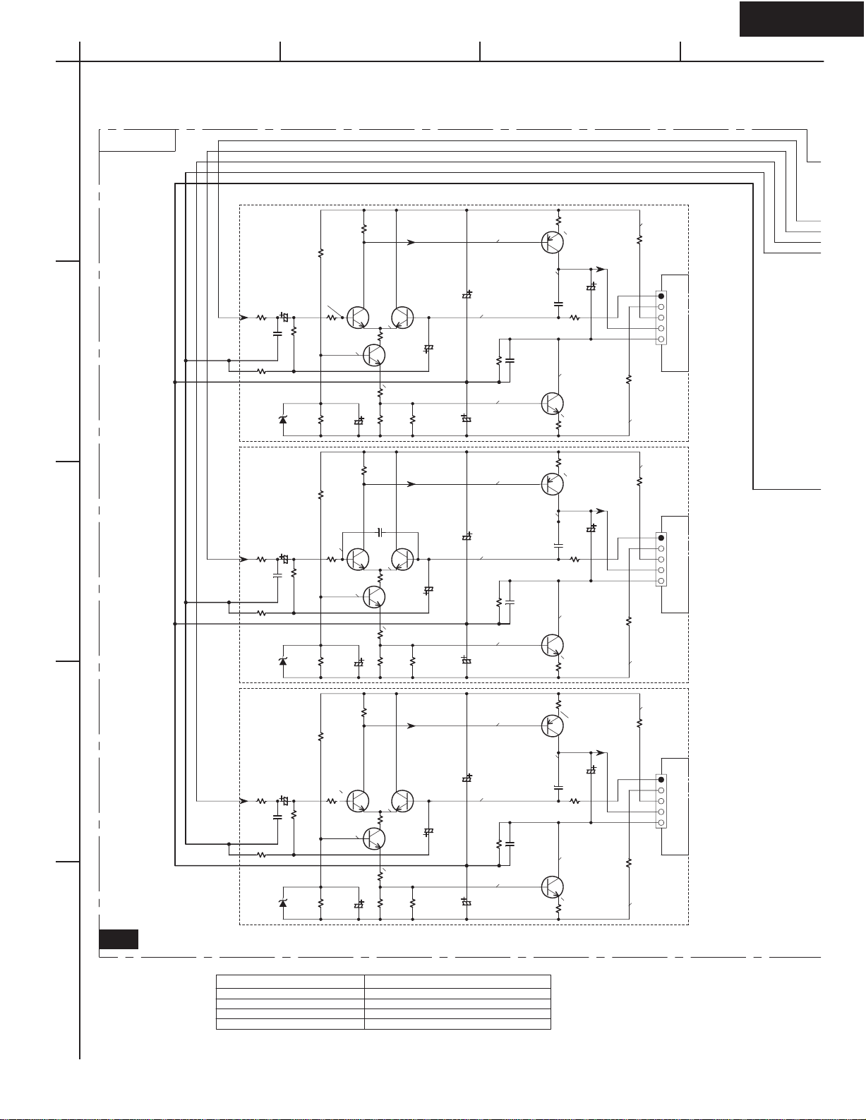
SCHEMATIC DIAGRAM 4-1 Power amplifier section
NAAF-7842
SL
1
(SCH-3)
TO NAAF-7830
SR
2
(SCH-3)
TO NAAF-7830
SB
3
(SCH-3)
TO NAAF-7830
R6033
390
5.6K
P6003
3.9K
NF
-B1 E
+B1
B+ E
R6043
B- E
1K
3.9K
390
5.6K
P6004
3.9K
NF
-B1
+B1
B+
B-
R6035
390
5.6K
P6005
3.9K
NF
-B1
+B1
B+
B-
R6003
[0.2V]
R6013
Q6013
[-0.3V]
R6053
R6034
R6004
[0.2V]
R6014
R6044
1K
[-0.3V]
R6054
3.9K
R6005
[0.2V]
R6015
Q6015
R6045
1K
[-0.3V]
R6055
3.9K
[1V]
[-0.3V]
[-58.2V]
[1V]
Q6014
[-0.3V]
[-58.2V]
[1V]
[-0.3V]
[-58.2V]
[1.1V]
Q6023
[-1.1V]
[1.1V]
Q6024
[-1.1V]
[1.1V]
Q6025
[-1.1V]
[0.5V]
R6073
110
(1/4W)
[-0.5V]
Q6043
[0.5V]
R6074
110
(1/4W)
[-0.5V]
Q6044
[0.5V]
R6075
110
(1/4W)
[-0.5V]
Q6045
Q6033
C6043
Q6034
C6044
Q6035
C6045
47/50
R6083
2.2
(1/4W)
P6083
ID+
ID-
47/50
P6084
ID+
ID-
47/50
R6085
(1/4W)
P6085
ID+
ID-
R6093
2.2
(1/4W)
C6233
473J
R6233
(1W)
8.2
R6084
2.2
(1/4W)
R6094
2.2
(1/4W)
C6234
473J
R6234
(1W)
8.2
2.2
R6095
2.2
(1/4W)
C6235
473J
R6235
(1W)
8.2
[-0.5V]
[-0.5V]
[-0.5V]
[0.5V]
[0V]
R6103
0.22X2
(2W)
[0.5V]
[0V]
R6104
0.22X2
(2W)
[0.5V]
[0V]
R6105
0.22X2
(2W)
[58.2V]
Q6053
R6143
22K
C6053
[0V]
Q6063
R6173
47K
D6003
[58.2V]
Q6054
R6144
22K
C6054
223J
R6154
[0V]
Q6064
R6174
47K
D6004
[58.2V]
Q6055
R6145
22K
C6055
223J
R6155
[0V]
Q6065
R6175
47K
D6005
R6163
Q6073
223J
R6153
12K
R6164
12K
R6165
Q6075
12K
33K
R6193
330K
D6013
R6183
47K
33K
Q6074
R6194
330K
D6014
R6184
47K
33K
R6195
330K
D6015
R6185
47K
E
E
E
(SCH-3)
TO NAAF-7830
E
E
E
P6011
4
5
10000/71
P6906
P931
+13VS
+13VS
MPUGND
MPUGND
(SCH-5)
POWER
TO NAPS-7845
C6901
10000/71
C6902
C6903
104J
C6708
223Z
D6903,6904:
D6903
D6904
R6905
R6904
RBV602
D5SBA20
RS603M
C6907
0
C6905
334J
/100
C6904
334J
/100
0
C6906
JL6951A
104J
104J
F6901
8A/125V
TO NAPS-7846
RL6902
D6906
RL6901
F6902
8A/125V
C6920
[0.1V]
JL6952A
TO NAPS-7846
[0.8V]
Q6901
R6605
8.2
(1/2W)
R6902
1K
SEMICONDUCTORS
NO.
Q6010-6015 2SC1740S-R,S
Q6020-6025 2SC1740S-R,S
Q6030-6035 KTD2061-Y OR 2SC5171
Q6040-6045 KTB1369-Y OR 2SA1930
Q6050-6055 KTC5242-O,R OR MN130S-Y,P,O OR 2SC5242-O,R
Q6060-6065 KTA1962-O,R OR MP130S-Y,P,O OR 2SA1962-O,R
Q6070-6075 2SC2631-R,S
Q6601-6603,Q6901 KTC3199-GR,2SC1740S-R,S,2SC2458-GR
Q6701,6702 KTC3200-BL,GR OR 2SC1775A-E,F OR 2SC1845-E,F
Q6703 KTA1268-GR,BL OR 2SA992-E,F
Q6303
KTA1267-GR OR 2SA933S-R,S
Page 20

HT-R510
A
BCD
SCHEMATIC DIAGRAM 4-2 Power amplifier section
1
2
3
4
L
P6000
NF
-B1
+B1
B+
(SCH-3)
R6040
B-
TO NAAF-7830
R6050
R
R6031
P6001
NF
-B1
+B1
B+
(SCH-3)
B-
TO NAAF-7830
C
P6002
NF
-B1
+B1
B+
(SCH-3)
B-
TO NAAF-7830
R6030
390
R6000
R6010
1K
3.9K
390
R6001
R6011
R6041
R6051
R6032
390
R6002
R6012
R6042
R6052
5.6K
3.9K
5.6K
3.9K
1K
3.9K
5.6K
3.9K
1K
3.9K
[1V]
[0.2V]
Q6010
[-0.3V]
[-58.2V]
[1V]
[0.2V]
Q6011
[-0.3V]
[-58.2V]
[1V]
[0.2V]
Q6012
[-0.3V]
[-58.2V]
[1.1V]
[-0.3V]
[1.1V]
[-0.3V]
[1.1V]
[-0.3V]
[0.5V]
R6070
110
(1/4W)
Q6020
[-0.5V]
[-1.1V]
Q6040
[0.5V]
R6071
(1/4W)
Q6021
[-0.5V]
[-1.1V]
Q6041
[0.5V]
R6072
110
(1/4W)
Q6022
[-0.5V]
[-1.1V]
Q6042
110
Q6030
47/50
C6040
Q6031
C6041
47/50
Q6032
47/50
C6042
R6080
2.2
(1/4W)
P6080
ID+
ID-
R6090
2.2
(1/4W)
C6230
R6230
8.2
R6081
2.2
(1/4W)
P6081
ID+
ID-
R6091
2.2
(1/4W)
C6231
R6231
8.2
R6082
2.2
(1/4W)
P6082
ID+
ID-
R6092
2.2
(1/4W)
C6232
473J
R6232
8.2
[0.5V]
[-0.5V]
473J
(1W)
[0.5V]
[-0.5V]
473J
(1W)
[0.5V]
[-0.5V]
(1W)
[0V]
R6100
0.22X2
(2W)
[0V]
R6101
0.22X2
(2W)
[0V]
R6102
0.22X2
(2W)
[58.2V]
Q6050
R6140
22K
C6050
R6150
[0V]
Q6060
R6170
D6000
48.6V
Q6051
R6141
22K
C6051
223J
[0V]
Q6061
R6171
47K
[58.2V]
Q6052
R6142
22K
C6052
[0V]
Q6062
R6172
47K
D6002
R6160
Q6070
223J
12K
47K
R6161
Q6071
R6151
12K
D6001
Q6072
223J
R6152
12K
33K
R6190
330K
D6010
R6180
47K
33K
R6191
330K
D6011
R6181
47K
R6162
33K
R6192
330K
D6012
R6182
47K
R6317
2.2K
R6306
P6301
10K
TH2
D6307
R6851
390
(1/2W)
COM
TH2
D6306
R6307
TH1
TH1
+24V
Q6303
2.2K
U21
[PTH9M04BF222TS2F333]
NAETC-7849
JL6402B
JL6402A
THERMISTOR
R6380
24V
0V
R6308
4.7K
JL6804A
LSPE
RSPE
CSPE
LSSPE
RSSPE
SBSPE
LSP
RSP
CSP
LSSP
RSSP
SBSP
R6850
390
(1/2W)
(SCH-5)
TO NAETC-7835
(SCH-5)
TO NAETC-7835
JL6803A
R6702
C6703
10K
R6708
33K
[0V]
Q6701 Q6702
D6701
C6701
220/6.3
223Z
R6701
22K
5
C6704
1/50
D6702
+B1
Q6703
[0V]
R6704
47K
D6703
MTZJ5.1B
C6706
100/6.3
R6706
220K
D6704
MTZJ5.1B
5.6K
R6709
0.05V
R66011KR6603
R6710
12K
+13VS
POWER
24V
0.8V
1K
24V
Q6602Q6603Q6601
0V 0V
R6602
1K
8.2
R6604
MPUGND
MPUGND
VOLH
SEC1H
SPB
SPCS
SPF
PRO
POWER
+13VS
RLGND
PROTHERM
BRLD
FRLD
CSRLD
+24V
(1/2W)
HPL
HPR
E
+24V
JL6805A
(SCH-5)
TO NAETC-7835
P6931NCETC-7833
(SCH-5)
Page 21

HT-R510
A
BCD
SCHEMATIC DIAGRAM 5-1 Power supply and Speaker terminal sections
RL6600
RL6601
D6601
C6601
RL6604
D6604
C6600
103J
D6600
103Z
C6604
103J
RL6603
L
R
FRONT SPEAKER
U10
SL
SR
CENTER
SB
SPEAKER-B
P6802
SURROUND
SPEAKER
NAETC-7835
1
JL6803B
LSP
RSP
CSP
LSSP
RSSP
(SCH-4)
TO NAAF-7842
SBSP
2
JL6805B
BRLD
FRLD
CSRLD
(SCH-4)
+24V
3
TO NAAF-7842
LSPE
RSPE
CSPE
JL6804B
LSSPE
RSSPE
SBSPE
TO NAAF-7842
(SCH-4)
C922
C921
220/35
223Z
R924
D921
D922
E921
4
P901
AC-H
AC-G
P901A
223Z
D923
C923
D921-D924
GP104003E OR
RL1N4003
T902
NPT-1358D
R901
3.3M
D924
U24
5
R926
4.7K
82
(1/2W)
2SC2458-GR
D925
2SC1740S-R,S
0.1V
RL901
P902
120W
NAPS-7845
+13VS
+13VS
MPUGND
MPUGND
POWER
Q921
1K
R923
C901
103M
/275VAC
P912
F901
8A/125V
AC OUTLET
1A MAX
P911
(SCH-4)
TO NNAF-7842
P931A
U23
P912A
3
NAPS-7844
7
P911A
T901
NPT-1465D
THERMAL FUSE
NAETC-7834
8
9
U13
10
11
12
13
14
15
16
17
18
19
JL6951B
TO NAAF-7842
(SCH-4)
(1/2W)
R9502
0.47(1/2W)
R9501
1
R9503
TO NAAF-7842
3.3
C9513
223Z
(1/2W)
(1/2W)
0.22
NAPS-7846
(SCH-4)
JL9501B
U25
JL6952B
Page 22

A
BCD
SCHEMATIC DIAGRAM 5-2 Power supply and Speaker terminal sections
NAETC-7833
1
Q6931
NJM78M56FA
17.8V
D6933
R6935
120
2
3
(2W)
PROTHERM
S3GND
+13VS
POWER
P6931A TO NAAF-7842
U12
5.6V
C6933
10/16
O
G
I
C6932
103Z
C6931
1000/25
D6932
D6932,6933:
GP104003E OR
RL1N4003
PRO
SPF
SPB
SPCS
SE1H
VOLH
(SCH-4)
MPUGND
MPUGND
+24V
AGND
HPR
HPL
PROTHERM
FLAC1
FLAC2
MPUGND
MPUGND
HPL
AGND
HPR
+5.6V
+24V
S3
S3GND
S3GND
+5.6V
POWER
SPF
SPCS
SE1H
SPB
VOLH
PRO
MPUGND
+13VS
S3
S2
S2
S2
S2
P7503B
(SCH-1)
TO NADIS-7403
P410A
(SCH-2)
TO NADG-7821
P411A
(SCH-2)
TO NADG-7821
JL9501A
4
THIS SYMBOL LOCATED NEAR THE FUSE INDICATES
THAT THE FUSE USED IS SLOW OPERATING TYPE
5
FOR CONTINUED PROTECTION AGAINST FIRE
HAZARD,REPLACE WITH SAME TYPE FUSE. FOR FUSE
RATING REFER TO THE MARKING ADJACENT TO THE SYMBOL
CE SYMBOLE INDIQUE QUE LE FUSIBLE UTLISE EST
E LENT. POUR UNE PROTECTION PERMANENTE,N'UTILISER
QUE DES FUSIBLES DE MEME TYPE. CE DARNIER EST
INDIQUE LA QU LE PRESENT SYMBOL EST APPOSE.
CAUTION
FOR CONTINUED PROTECTION
AGAINST FIRE HAZARD, REPLACE
ONLY WITH FUSE OF SAME TYPE
VA
AND RATING INDICATED.
ATTENTION
AFIN D'ASSURER UNE PROTECTION
PERMANENTE CONTRE LES RISQUES
D'INCENDIE, REMPLACER UNIQUEMENT
VA
PAR UN FUSIBLE DE MEME TYPE
ET CALIBRATION COMME INDIQUE.
Page 23

HT-R510
A
SCHEMATIC DIAGRAM 6
Video section
NAVD-7831
1
COMPONENT
COMPONENT
2
IN 2
IN1
CR(PR)
CB(PB)
Y
P241
CR(PR)
CB(PB)
Y
P241
BCD
U10
COMPONENT OUT
CR
R249
1K
D241
C241
103Z
RL242
RL241
Q241
2SC1740
P241
C242
103Z
CB
Y
+5V
DGND
DGND
P243B
CNPT
TO NAETC-7838
3
4
5
Page 24

HT-R510
1
3
A
PRINTED CIRCUIT BOARD VIEW 1
NADIS-7403,Display circuit PC board
U3
1
P7502A
SBMDI
SBMDO
SBMCLK
HPDET
SBMLDY
S7501
S7501
GND
SYSIN
J7548
J7544
12
15
J7549
J7538
J7526
-VP
HPMUT
SBMRST
2
NCDIS-7403
25137403B
1
Component side
BCD
P7503A
HPR
HPE
HPL
GND
GND
FLAC
FLAC
+5.6V
22
S7641
22
S7643
J7537
J7542
C7521
17
J7518
J7501
C7502
U7501
VCC
J7527
J7513
C7514
30
J7529
S7631
7
J7514
2
SP
ADJUST
J7530
S7632 S7633
CD
STEREO DIRECT
J7539
7
J7511
ADJUST
J7510
J7543
S7642
DSP SURROUND
S7644
PRESET
ADJUST
22
S7645
AUDIO
2
S7646
J7552
S7647
J7502
J7524
15
GND
VOUT
J7553
12
J7515
J7519
TUNER TAPE
S7637
TUNING TUNING FM
UP DOWN
30
17
J7523
S7634
R7580
J7525
27
J7528
S7636
22
J7512
2
MODE
15
J7554
S7635
J7540
Q750
7
J7522
J75
20
3
222
SYSIN
HPMUT
SBMLDY
SBMRST
SBMCLK
HPDET
SBMDO
SBMDI
GND
-VP
4
C7515
R7527
R7526
C7516
R7644
L7504
+5.6V
R7643
R7645
FLAC
FLAC
GND
GND
HPL
HPE
HPR
L7505
R7641
C7505
D7507
D7501
C7504
C7517
R7631
R7642
R7646
C7503
R7502
C7506
C7501
R7501
R7636
R7503
R7635
Q7503
61
R7634
Soldering side
5
R7632
R7633
Page 25

HT-R510
A
PRINTED CIRCUIT BOARD VIEW 1
1
C7512
S7626
VIDEO3
R7581
X7501
J7536
J7533
7
J7534
15
S7611 S7612
2
DIGITAL
INPUT
S7625
501
Q7501
2
S7627
2
7535
0
MEMORY
7
J7521
15
12
J7504
J7503
R7582
J7541
7
2
SW
MODE
17
3
BCD
7
J7509
J7520
22
J7517
J7516
20
22
S7613 S7621
DIMMER DISPLAY
J7508
22
J7532
15
J7531
S7623S7624
DVDVIDEO1VIDEO2
7
J7545
J7551
7
J7547
D7505
SELECTER
J7506
J7507
S7622
AUDIO
22222
RL7501
12
12
J7550
J7546
HPR
HPE
HPL
GND
HPDET
JL7501A
U5
JL7502A
NAETC-7405,Headphone
terminal PC board
E7501
J7573
J7572
J7571
R
L
P7501
P7501
J7574
JL7502B
0
NCETC-7405
25137405
Component side
C7518
L7503750
L7502
L750
L7501
C77519
R
C7520
C
L
Soldering side
Q7507
D7503
D7502
R7532
R7504
R7530
Q7504
R7512
R7529
R7528
R7517
R7518
R7505
R7516
R7611
R7515
R7511
R7510
C7511
R7509
R7523
R7508
R7522
R7612
R7507
C7510
R7521
C7509
R7506
C7508
R7520
R7531
R7621
41
4
Q750
R7626
2
C7513
Q7502
1
C7507
21
R7513
R7514
R7524
C7523
C7522
D7504
Q7506
R7519
5
U17
R7625
R7624
R7623
R7622
P243A
+5V
CNPT
DGND
DGND
P206A
GND
+12V
GND
CNPT
CTLA
7
0
CTLB
VMUT2
VMUT1
J301
NCETC-7838
25137838
P801B
RI
+5V
DGND
OPT1
OPT2
COAX
OPTOUT
NAETC-7838,Connector
PC board ass'y
Page 26

HT-R510
7
7
7
7
7
7
C
010
7
9
0
1
7
7
7
7
7
7
7
7
7
7
7
7
7
7
7
7
7
R7044
R7120
7
7
7
A
PRINTED CIRCUIT BOARD VIEW 2
1
U1
2
3
4
NADG-7821, DSP circuit PC board
D9510
D9512
D9509
D9511
C9505
C9505
C6401
P6403
C9502
D9504
D9505
D9502
D9503
R6408
R6407
Q6405
C9503
C9501
P410B P411B
1
BCD
Q7004
R730
R7051
R729
R715
R7050
R7012
R728
R716
R7015
R727
R717
R7049
R7016
R726
R7048
R7017
Q701
R7047
R7018
R7146
R7046
R7019
R72
R72
R71
R7045
R
R
R
R
R
R
R
R
R
R
R
R
R
R
R
R
R7020
R
R
R
R
C
C
C
C
R
C
C
7
C6410
C6409
C9507
C9507
C9506
C9506
D9506
D9507
R6402
C9510
R6403
C6404
C6403
R9508
R9507
D9508
C9511
Q6402
C9508
R6410
C9510
Q9501
C6406
Q6403
R9506
C9512
C6405
C9508
R760
R758
R9509
P802
R759
C733
Q706
R745
C728
C6412
R747
R742
C730
R744
P7502B
C727
C722
Q706
C729
R761
1
R743
C726
P412B
1
P7502B
C7015
1
Q703
R731
R732
C6411
R733
Q6406
R734
C184
R735
L181
Q702
R736
C185
C183
C182
R737
R738
R181
Q703
C181
X181
C186
Q181
L7002
R183
R186
R182
R7062
R7063
R7064
R7065
R7066
C7008
R185
1
Q181
Q702
C187
R746
R740
C7001
R184
Q705
1
1
Q704
C732
R187
L7001
C7005
Q705
Q704
C717
D7702
D7003
C7009
R7076
R7077
R7083
R7085
C7011
C7012
Q710
Q710
C7004
R748
R754
R755
R756
R757
1
R7033
R7000
R7071
C731
C720
1
R7080
C721
R751
R752
R753
C704
C7002
C701
R706
Q7003
Q7003
D7004
C7007
R7178
R7078
R7179
R7079
R7180
R702
C705
Q7008
R705
C702
R750
C703
L703
R707
R704
R709
C7006
X7001
C7003
R7003
D7002
R749
R703
R708
R7060
Q7001
D7001
R701
C714
R710
R7059
C7014
R7056
1
L701
R711
R7058
R7001
P7701
R712
R7057
R7055
R7002
Q701
R713
R7054
R7004
1
R7053
Q7008
C707
1
R714
Q7002
Q7002
R7052
R7011
5
Page 27

HT-R510
0
0
A
BCD
PRINTED CIRCUIT BOARD VIEW 2
1
U1
2
R751
R752
R753
C7002
C704
R706
Q7003
Q7003
D7004
C701
C7007
R7178
R7078
R7179
R7079
R7180
R702
C705
Q7008
R705
C702
R750
C703
L703
R707
R704
C7006
X7001
R709
R749
C7003
R7003
D7002
R703
R708
R7060
D7001
C714
Q7001
C7014
R701
R710
R7059
1
L701
R711
R7058
R7056
R7001
P7701
R712
R7057
R7055
R7002
Q701
R713
1
R7054
R7004
C707
R7053
Q7008
1
R714
Q7002
Q7002
R7052
R7011
R730
R7051
R7012
R715
R729
R7050
R728
R716
R7015
R727
R717
R7049
R7016
R726
R7048
R7017
C7011
C731
C721
R748
C720
R754
R755
R756
R757
3
1
83
85
1
004
R7033
3
R7000
R7071
9
76
77
4
R7080
NADG-7821, DSP circuit PC board
Q701
R7047
R7018
Q7004
R721
R720
R719
R7146
R7046
R7019
R7045
R7040
R7839
R7039
R7138
R7038
R7036
R7037
R7035
R7134
R7034
R7032
R7031
R7030
R7029
R7028
R7027
R7020
R725
R724
R723
R722
C713
C712
C711
C708
R718
C709
C710
C7010
R7044
R7120
R7075
R7043
L705
R7074
R7084
R7082
R7081
C706
R7042
R7073
R7072
R7041
L704
L706
R7070
R7141
L702
1
C106
R7025
R7024
R7023
R7022
R7021
R821
C716
C715
R7069
X701
Q707
R7068
R739
R7067
R7026
C817
C816
C101
L806
X801
R826
R105
R106
C105
P101
Q101
C802
C803
C804
C805
R801
L805
R803
R804
R805
R806
L804
C801
L803
Q321
C366
R807
R808
C188
C103
1
R809
R104
C359
R810
C104
R822
R823
R824
R825
R811
1
Q801
R812
Q322
P406
P306
C818
R813
R390
R814
Q314
Q307
R380R381
R377
C361
C821
Q805
C807
R379
R378
P261A
R815
Q801
C809
L801
C811
Q805
C808
C367
C363
C364
C810
Q311
Q310
Q309
Q308
C819
C820
C806
R389
R375
R397
R374
R396
R372
R331
R373
R344
R371
R330
C356
C353
C355
Q306
C357
C354
C360
L802
C362
R820
C815
C837
C834
C832
C374
C373
C371C372
C822
C836
R819
C814
C835
C833
R818
C813
C375
R364
C347
R365R366
R363
R817
C812
C348
R816
C800
R835
R832
C344
R836R837
R843
R840
R844R845
C848
C331
C851
C343
R848
C342
C340
C338
R851
C339
C337
C840
C341
R852R853
C332
C346
C345
C844C845
C843
P801
C335C336
R833R834
R841R842
Q804
Q803
Q802
C853
C849C850
R849R850
C330
C852
C841C842
C333
P305
R321
C321
R343
C320
R342
R320
R319
C319
R341
R340
C318
R318
C326
R317
C317
R339
R338
C316
D802
C358
Q313
R316
R315
C315
R337
R336
C314
R314
R313
C313
R335
R334
C312
R312
C325
R311
C311
R333
R332
C310
R310
C323
R307
C307
R329
R328
C306
R306
R305
C305
R327
R326
1
C304
R304
R303
C303
R325
R324
C302
R302
C322
R301
C301
R323
R322
C300
R388
E300
C334
C327
R359
R361
R856
R367
R855
C350
C861
R368
R854
R369
Q323
Q323
C862
R370
R858
R857
C860
1
Q305
1
R383
C351
C349
C376
R360
R386
R348
Q302
1
C328
R362
1
C863
1
C859
C858
C857
R387
1
R347
C856
C855
1
C854
NCDG-7821
25137821A
Q301
Q301
1
C329
R345
R102
R103
R346
Q7006
R384
Q7007
Q312
R376
D801
R300
C352
C365
R385
R382
P304
P302
P301
C308
P305
P304
P302
P301
P351
P351
5
Page 28

HT-R510
7
2
2
7
J
0
R
R
6
2
0
A
PRINTED CIRCUIT BOARD VIEW 4
Q6015
BCEBCE BCEBCEBCEBCEBCE
1
P6931
HPL
HPR
AGND
+24V
MPUGND
MPUGND
VOLH
SE1H
SPB
SPCS
SPF
PRO
15
J6191
POWER
+13VS
RLGND
THPRO
2
Q6065
R6095
12 17 20
J6190
D6015
17
R6850
R6851
Q6075
C6055
R6155
BE
R6145
D6005
R6185
R6175
R6165
P6005
J6189
15
R6105 R6104 R61
J6188
E
Q6025
E
J6187
Q6045
R6195
B
B
J6186
ID-ID+
R6055
NF
B+
B-
-B1
+B1
SB
27
Q6035
J6185
20
B
17
17
17
E
R6025
Q6055
J6179
J6183
J6180
J6181
R6075
R6035
R6085
R6015
R6005
P6072A
J6184
J6182
C6045
D6014
Q6074
D6004
BCD
Q6014
R6094
1227
J6175J6178
12
J6172 J6161
17
J6171
17
J6170
15
J6174
E
E
B
R6174
R6154
R6144
R6164
R6184
NF
C6054
-B1
Q6024
E
J6169
Q6044
R6194
B
B
P6084P6085 P6082
B+
+B1
Q6034
J6168
ID-ID+
R6054
P6004
B-
Q6054
J6159
J6160J6176
J6162
J6163
R6074
R6014
R6004
R6024
R6034
22
R6084
J6158
C6044
J6165
J6152
Q6073
D6003
D6013
EB
R6153
R6173
R6143
J6166
25
25
12
12
25
B
E
C6053
R6163
R6193
R6183
12
12
17
P6083
NF
J6146
-B1
2020
J6150
J6151
17
Q6063
17
17
15
E
Q6043
B
+B1
B+
LSRS
7
J6155
D6714
C6716
J6167
R6719
J6157
J6156
J6154
J6142
Q6013
EEEBBBB
15221525
25
25
B
E
R6023
0
20
15
15
12
12
R6073
R6013
R6003
R6033
J6141
J6130
J6131
J6138J6149J6164J6173
J6136
R6083
Q6053
J6132
J6135
J6139
J6137
J6133
J6134
C6043
Q6072
BE
R6172
D6002
B+
-B1
+B1
NF
C
NCAF-7842
22
D6012
12
J6125
27
J6115
R6152
R6192
C6052
R6142 J6116
R6162
R6182
B-
25
R6318
R6093
J6153J6177
J6148
J6143
J6144
ID-ID+
R6103
J6147
J6140
Q6023
E
Q6033
B
J6145
R6053
R6043R6044R6045 R6042
B-
P6003
25137842
J6128
J6129
17
25
J6126
20
J6127
E
Q6042
B
J6124
Q601
Q6062Q6064
R6092
J6123
15
J6121
17
J6119
17
J6120
J6114
25
B
Q6022
E
Q6032
B
E
R6072
ID-ID+
R6052
P6002
P6073A
R6022
J6111
R
J6109
J6110
U21
NAAF-7842,Power amplifier PC board
3
J61
7
R6380
ETC7849
25137849
4
JL6402B
0
U28
NAETC-7849,Thermal det. PC board
R6381
NCETC-7850
25137850
0
J6501
TH1
+24V
TH2
J6502
C6904C6905
P6909
5
Page 29

HT-R510
Q6033
A
BCD
PRINTED CIRCUIT BOARD VIEW 4
R6091
J6080
J6078
J6075
J6076
J6077
J6072
E
B
25
22
P995A
30
JL6952
POWER
Q6031
P6903
27
25
J6070
MPUGND
P931
Q6011
22
B
E
R6021
J6066
30
30
J6063
J6062
J6102
J6082
MPUGND
+13VS
+13VS
15
R6071
R6011
R6001
R6031
J6071
J6046
J6067
J6068
J6069
P6922
RL6902
25
25
30
27
27
J6058
J6050
R6081
P6011A
J6061
J6064
J6065
RL6902
J6037
20
30
Q6051
J6060
J6053
J6054
J6055
12
J6057
20
17
J6056
17
J6049
J6051
Q6070
BE
R6170
D6000
B
Q6701
JL6804A
LSSPE
RSSPE
SBSPE
20
17
D6904
27
J6036
J6035
J6052
R6140
R6160
7
RSPE
CSPE
C6901
C6901
30
30
J6034
R6150
R6180
J6047
D6702
B
EE
LSPE
25
J6059
15
J6025
J6022
C6050
R6701
7
J6042
J6043
12
D6010
P6080
NF
Q6702
7
J6045
J6039
22
22
25
R6190
-B1
P6000
D6701
J6044
J6038
J6048
+B1
27
J6033
E
Q6040
B
ID-ID+
B+
R6708
C6701
22
J6041
C6906
17
17
15
J6031
J6032
R6709
Q6013
1
25
25
15
20
R6103
15
15
12
12
R6073
EB
R6013
R6003
R6023
2
R6033
43 R6042 R6041 R6040
J6141
J6130
J6131
J6138
R6083
J6135
J6136
J6139
J6137
J6133
J6134
C6043
J6132
D6012
12
R6152
Q6072
R6142 J6116
BE
R6172
D6002
R6162
B+
B-
-B1
+B1
NF
25
C
0
NCAF-7842
Q6062
20
J6128
J6129
22
J6127 J6117
17
17
17
25
J6125
27
J6115 J6113
E
J6126
Q6042
R6192
C6052
B
ID-ID+
R6182
P6082
R6318
R6052
P6002
J6124
25137842
Q6012
BCEBCEBCEBCEBCEBCEBCE
R6092
R6102 R6101 R6100
J6119
J6120
J6114
25
B
Q6022
E
Q6032
B
E
P6073A
J6111
Q6052
J6098
17
17
R6306
R6706
J6094
J6095
J6097J6121
D6001
R6317
C6704
R6704
J6096
J6091
Q6071
R6171
P6001
R6307
EB
J6099
R6141
R6161
D6703
D6307
J6089
R6181 R6151
NF
D6306
J6088
D6011
12
J6073
C6051
P6081
-B1
Q6303
J6122J6123
27
27
15
20
12
J6118
J6112
C6042 C6041 C6040
R6072
R6082
R6012
R6002
R6022
R6032
Q6313
EB
J6109
7
J6110
J6108
22
25
R6191
+B1
BE
J6090
B+
J6092
J6093
J6079
17
E
Q6041
B
ID-ID+
B-
COM
P6301
20
20
R
TH1
TH2
20
17
R6051
R6308
Q6061
17
Q6021
J6074
U21
NAAF-7842,Power
3
amplifier PC board
4
5
C6904C6905
P6909
J6107
7
J011
7
J6106
J6105
R6905
J6100
P996A
D6706
C6708
D6705
15
J6104
R6904
J6101
RL6901
1A
5
69
L
J
C6902
C6902
15
J6087
27
J6103
D6903
RL6901
7
7
C6908
15
P997A
J6086
15
P6907
J6085
J6084
P995B
7
J6083
A
J6081
J6029
J6023
R6050
B-
Q6703
E
25
J6018
J6016
J6015
20
17
17
Q6020
E
B
J6024
B
R6710
J6040
J6017
C6907
Q6060
J6027
R6702
C6706
20
R6090
J6026
Q6030
L
D6704
C6703
J010
P6923
R6235
D6901
Q6010
EEEEBBBB
Q6050Q6053
J6014
-B1
J011A
27
B
R6070
E
R6010
R6000
R6020
R6030
J6021
JL6402A
30
J6020
C6920
17
F6902
15
E
R6080
R6233
30
J6019
D6906
J6001
C6909
F6902B
F6902A
17
17
17
R6605
E
R6603
E
E
2017
15
15
J6012
J6005
J6006
TH1
TH2
R6234
J6002
J6003
Q6603
Q6602
Q6601
F6901A F6901B
R6902
J6007
+24V
R6604
J6013J6030
J6009J6028
J6010
J6011
R6232
R6602
B
B
B
R6601
E
B
J6004
R6231
R6230
Q6901
JL6805A
F6901
+B1
J010A
JL6803A
30
P6802
8A/125V
P6910
C6903
D6902
C6235
C6234
C6233
C6232
C6231
C6230
+24V
CSRLD
FRLD
BRLD
25
RSSP
SBSP
P6801
LSP
RSP
CSP
LSSP
J6008
P6906
Page 30

HT-R510
A
PRINTED CIRCUIT BOARD VIEW 5
1
C6604
D6604
C6855
SB-
C6842
C6852
RL6603
FRLD
BRLD
CSRLD
JL6805B
+24V
SB+
C-
RL6603
J5301
R6812
J5304
L6802
L6802
R6802
C6845
R6815
L6805
J5305
R6805
L6805
2
U14
3
25
J5202
J5201
S3
+24V
SPF
SPCS
POWER
SE1H
SPB
PRO
VOLH
+13VS
MPUGND
MPUGND
S3GND
P410AP411A
RS-
P6802
C+
P6802
J5302
RSSPE
SBSPE
J5303
D6600
LSSPE
RL6604
C6600
J5307
15
RL6604
J5306
C6854
15
27
RSPE
CSPE
LSPE
LS-
25
JL6804B
NAETC-7835,Speaker terminal PC board
C6932
OI
C6933
252525
25
17
J5204
S2
J5205
S2
J5207
J5206
S2
S2
+5.6V
PROTHERM
S3GND
J5203
S3
BCD
J5323
P6801
R6803
L6803
J5322
RL6601
L6803
P6801
R-
C6846
L6804
J5324
15
R6813
C6601
D6601
L+L-R+
J5326
R6814
L6804
J5325
R6804
22
LSSP
RSSP
SBSP
CSP
RSP
RL6601
LSP
30
J5213
12
J5212
C6853
Q6931
R6932
J5208
RS+
HPR
+5.6V
C6844
J5313
AGND
HPL
MPUGND
R6935
LS+
C6843
J5314
RL6600
J5309
J5308
J5310
J5311
FLAC1
FLAC2
MPUGND
D6933
C6851
30
12
15
7
P7503B
C6931
C6931
D6932
R-
17
1
P7503B
C6850
P6800
NCETC-7835
25137835
R6933
J5209
L-
RL6600
30
15
J5210
P6800
L6801
J5312
20
J5211
R6811
J5316
J5317
R+
C6841
L6801
25
J5315
20
J5318
R6801
C6840
15
JL6803B
L+
R6810
L6800
J5320
R6800
J5319
L6800
7
J5321
U12
NAETC-7833,Const. Voltage circuit PC board
4
5
P913A
J6202
P912A
NCPS-7844
25137844
0
J6203
5
U23
NAPS-7844,Transformer terminal PC board
731
J6201
P911A
Page 31

HT-R510
12
A
PRINTED CIRCUIT
BO ARD VIEW 5
1
2
NCETC-7833
25137833
0
30
30
30
3
J5213
J5214
J5215
S3E
BCD
NCPS-7845
0
25137845
P901A
AC-H
J6310
30
T2.5AL250V
F903
22
J6319
J6318
15
C901
C901
RL901
MPUGND
MPUGND
POWER
+13VS
+13VS
R923
C923
R926
C922
S4
S4
S3
JL9501
S3
12
S2
S2
J5218
RL901
R922
D922
D924
R924
B
Q921
E
D921
D923
P931A
U24
J6320
D925
C921
R921
15
F903B
J6312
15
J6311
J6315
7
J6316
7
P921
F901B
J6317
7
F902B
578
56789
NAPS-7845,Primary circuit PC board
F903A
6.3A/125V
P922
F901
J6313
F902
P923
T902
7
P909 P908
P912
F901A
F902A
P913
1234
AC-G
AC-GAC-H
J6305
25
J6304
25
J6314
C902
30
C902
T3.15AL250V
P917
J6308
7
T902
P918
12
J6306
7
J6307
J6302
17
P911
P902
J6303
J6309
7
15
P921A
17
R901
P926
J6301
P925
P922A
120V 220V
P923A
E921
NNLL
P902
S902
S902
J5212
NCPS-7846
25137846
J6405
J6402
17
J6401
15
J6407
12
12
J6403
JL6952B
15
0
J6404
P996
J6410
20
HPL
HPR
AGND
+24V
MPUGND
J5216
J5217
VOLH
MPUGND
NCETC-7834
25137834
SE1H
SPB
7
SPCS
SPF
PRO
F9501
POWER
+13VS
RLGND
PROTHERM
141312111098
0
U25
NAPS-7846,Secondary terminal PC board
P6931A
4
J6408
P995
J6406
J6409
JL6951B
1918171615
J6411
J6412
P997
J6413
1.6A/125V
F9501A
R9501
C9513
R9502
JL9501B
R9521
5
U13
NAPS-7834,Secondary circuit PC board
F9501B
R9503
Page 32

HT-R510
A
PRINTED CIRCUIT BOARD VIEW 3
Video section
1
A
B
7
RI
GND
GND
VM2
+12V
CNPT
P253A
P253A
C218
C221
J209
J210
J211
J240
12
C223
J206 J207 J208
C225
J204 J205
12
J203
15 15
J202
2
3
VM1
J237
12
OPT2
J230
J238
C219
Q205 Q206
C217
J229
17
20
C224
J232
J231
Q212
R209
R230
C222
R207
R208
15
Q204
Q203
R227
R229
C226
R225
J219
J222
R228
Q209
Q213
OPT1
DGND
R223
7
J227
R210
7
J226
12
R226
4
U26
NAVD-7847,Video circuit PC board
5
+5V
J228
20
COAX
J223
J241
J213
Q210
Q211
P299
OPTOUT
L281
R224
J242
Q201
Q207
Q208
17
J212
7
15
J215
Q202
L282
J233
P206B
7
J220
J225
C214
C205
J243
12
J221
C202
J236
7
C203
C204
15
J216
C285
C286
J217
12
17
0
L283
J239
NCVD-7847
25137847
J224
C206
R212
C201
R201
C207
C210
C211
C208
C209
C212
C213
R221
R206
C215
BCD
E
D5000
R5100
R5090
C5070
J5010
J5012
D5001
R5101
R5091
C5071
D5002
R5102
R5092
C5072
D5003
R5103
R5093
C5073
D5004
R5104
R5094
C5074
D5005
R5105
R5095
C5075
C5020
Q5030
BBE
J5005
J5007
J5011
C5021
Q5031
BBE
C5022
Q5032
BBE
C5023
Q5033
BBE
C5024
Q5034
BBE
C5025
Q5035
B
R5060
C5100
R5061
C5101
R5062
C5102
R5063
C5103
R5064
C5104
R5065
C5105
E
R5170
R5070
R5080
C5090
R5130
30
30
R5171
R5071
R5081
C5091
R5131
R5172
R5072
R5082
C5092
R5132
R5173
R5073
R5083
C5093
R5133
R5174
R5074
R5084
C5094
R5134
R5175
R5075
R5085
C5095
R5135
J5002
C5110
30
J5021
C5111
J5028
C5112
J5036
C5113
J5044
C5114
J5049
C5115
Q5040
R5180
R5160
R5190
30
30
P5001
J5009
27
27
E
Q5041
J5019
R5181
R5161
R5191
E
Q5042
J5026
R5182
R5162
R5192
E
Q5043
R5183
R5163
R5193
E
Q5044
R5184
R5164
R5194
P6073
EB
Q5045
R5185
R5165
R5195
C5050
20
C5051
B+
+B1
-B1
NF
B+
+B1
-B1
NF
C5052
B+
+B1
C5053
-B1
NF
C5054
B-
B+
-B1
+B1
NF
C5055
+B1
B-
B+
+B1
-B1
NF
J5001
B-
30
J5020
B-
J5027
7
B-
2225 15
J5035
J5039
15
J5043
B-
B+
-B1
NF
P6000A
P6011A
P6001A
J5023
P6002A
J5031
P6003A
P6004A
J5046
P6005A
7
7
1
12
Q281
C284
R284
C283
R211
U9
J244
J245
J218
C288
J246J248
C282
R281
C287
R282
C281
R219
D201
D202
C227
R205
P201
R220
R214
R202
R213
R216
C220
R203
P203
R215
R218
P202
R222
R204
R217
C216
P204
NAAF-7830,
Driver circuit
PC board
C289
J247
12
P281
P202
U283
U282
U281
P282
P281
P201
P203
P204
U283
U282
U281
P282
E
E
E
Q5000
Q5010
R5050
R5020
R5010
C5010
R5000
C5000
E
B
C5011
R5001
C5001
E
B
C5012
R5002
C5002
E
B
C5013
R5003
C5003
E
B
C5014
R5004
C5004
E
B
C5015
R5005
C5005
J5003
J5014
J5006
J5016
J5018
Q5011
E
J5022
R5021
R5011
E
B
J5030
R5022
R5012
E
B
J5038
R5023
R5013
E
B
J5045
R5024
R5014
J5050
R5025
R5015
B
B
Q5012
Q5013
Q5014
Q5015
E
B
Q5050
C5040
C5030
C5080
7
7
7
R5051
Q5051
C5041
C5031
C5081
R5052
Q5052
C5042
C5032
C5082
R5053
Q5053
C5043
C5033
C5083
R5054
Q5054
C5044
C5034
C5084
R5055
Q5055
C5045
C5035
C5085
B
R5110
R5030
E
B
R5111
R5031
E
B
R5112
R5032
E
B
R5113
R5033
E
B
R5114
R5034
E
B
R5115
R5035
B
R5040
L
P407A
P306A
E
L
E
R
E
RS
E
LS
E
C
E
SB
NCAF-7830
J5004
7
J5013
J5017
12
Q5001
22
J5015
P306A
R5041
R
7
J5024
J5025
J5029
15
Q5002
R5042
CLS
30
J5033
J5032
20
J5037
J5034
Q5003
7
R5043
30
J5040 J5048
1
25137830A
J5042
J5041
Q5004
7
R5044
30
RS
J5047
Q5005
25
R5045
SB
J5008
Page 33

K
K
IC BLOCK DIAGRAMS AND DESCRIPTIONS
AK4384(106dB 192kHz 24-Bit 2ch DAC )
HT-R510
SMUTE/CSN
ACKS/CCLK
DIF0/CDTI
LRC
BIC
SDTI
P/S
µP
Interface
Audio
ATT
De-emphasis
Control
8X
Interpolator
MCLK
Clock
Divider
Modulator
SCF
LPF
Data
Interface
PDN
ATT
8X
Interpolator
Modulator
SCF
LPF
No. Pin Name I/O Function
1 MCLK I Master Clock Input Pin
An external TTL clock should be input on this pin.
2 BICK I Audio Serial Data Clock Pin
3 SDTI I Audio Serial Data Input Pin
4 LRCK I L/R Clock Pin
5 PDN I Power -Down Mode Pin
When at “L”, the AK4384 is in the power-down mode and is held in reset.
The AK4384 should always be reset upon power-up.
SMUTE I Soft Mute Pin in parallel mode
6
“H”: Enable, “L ”: Disable
CSN I Chip Select Pin in serial mode
ACKS I Auto Setting Mode Pin in parallel mode
7
“L ”: Manual Setting Mode, “H”: Auto Setting Mode
CCLK I Control Data Clock Pin in serial mode
DIF0 I Audio Data Interface Format Pin in parallel mode 8
CDTI I Control Data Input Pin in serial mode
9 P/S I
Parallel/Serial Select Pin (Internal pull-up pin)
“L”: Serial control mode, “H”: Parallel control mode
10 AOUT R O Rch Analog Output Pin
11 AOUTL O Lch Analog Output Pin
12 VCOM O Common Voltage Pin, VDD/2
Normally connected to VSS with a 0.1mF c
a 10m F electrolytic cap.
13 VSS - Ground Pin
14 VDD - Power Supply Pin
15 DZFR O Rch Data Zero Input Detect Pin
16 DZFL O Lch Data Zero Input Detect Pin
VDD
VSS
VCOM
DZFL
DZFR
AOUTL
AOUTR
MCLK
BICK
SDTI
LRCK
PDN
SMUTE/CSN
ACKS/CCLK
DIF0/CDTI
m
F c
1
2
3
4
Top
View
5
6
7
8
16
15
14
13
12
11
10
DZFL
DZFR
VDD
VSS
VCOM
AOUTL
AOUTR
P/S
9
eramic capacitor in parallel with
Page 34

y
y
p
pply p
g
pply p
p
p
p
p
p
p
p
p
p
p
p
)
)
)
)
)
)
)
)
p
g g
pply p
g
g
p
g
g
g
g
g
g
g
g
p
p
g
p
p
p
p
p
p
p
p
IC BLOCK DIAGRAMS AND DESCRIPTIONS
AK4586VQ(96kHz 6ch CODEC)
PDN
RX1
I2C
RX2
TST
RX3
SLAVE
RX4
PVSSRPVDD
4443424140393837363534
XTO
XTI/EXTCLK
DVDD
DVSS
TVDD
TX
MCKO
LRCK
BICK
SDTO
SDTI1
LI
N
RIN
LOUT1
UT1
RO
LOUT
2
RO
UT2
3
LOUT
UT3
RO
1
2
3
4
5
6
7
8
9
10
11
AK4586VQ
Top View
1213141516171819202122
SDTI2
SDTI3
INT0
INT1
CAD1/CDTO
SDA/CDT1
Pin Layout
ADC
HP
F
C
LP
F
LP
F
F
LP
F
LP
LP
FDAC
FDAC
LP
AK4586VQ
AD
DAC
DA
DA
DA
F
HP
DATT
C
TT
DA
C
TT
DA
C
TT
DA
TT
DA
TT
DA
SCL/CCLK
CAD0/CSN
Audio
F
I/
MCLK
SDOUT
SDIN1
SDIN2
N3
SDI
DZF2/OVF
AVSS
CSN
uP I/F
Clock
Recovery
Decoder
33
32
31
30
29
28
27
26
25
24
23
AVDD
CCLK
DAIF
DEM
CDTI
RIN
LIN
ROUT1
LOUT1
ROUT2
LOUT2
ROUT3
LOUT3
DZF1
VCOM
VREFH
CDTO
X'tal
Oscillator
Clock
Generator
Input
Selector
XTI
XTO
CKO
M
TX
RX1
RX2
RX3
RX4
SDTO
BICK
LRCK
SDTI1
SDTI2
SDTI
No. Name I/O Description
1XTO O Cr
XTI I Cr
2
EXTCLK I Master clock in
3 TVDD - Power su
4 DVSS - Di
5 DVDD - Power su
6 TX O Transmitt er channel out
7 MCKO O Master clock out
8 LRCK I/O In
9 BICK I/O Audio serial data clock
10 S DTO O Audio serial data out
11 S DTI1 I A udi o serial data in
12 S DTI2 I A udi o serial data in
13 S DTI3 I A udi o serial data in
14 INT0 O Interru
15 INT1 O Interru
CDTO O Control data out
16
CADI I Chip address pin 1 (Bus mode
CDTI I Control data i nput pin (Serial mode
17
SDA I/O Control data input/output pin (Bus mode
CCLK I Control data clock pin (Serial mode
18
SCL I Control data c l ock pin (Bus mode
CSN I Chip select pin (Serial mode
19
CAD0 I Chip address pin 0 (Bus mode
DZF2 O Zero input detection pin 2
20
OVF O Overflow detection
21 AVSS - Analo
22 AVDD - Power su
23 VREFH I Reference volta
24 V COM O Com m on volta
25 DZF1 O Zero in
26 LOUT3 O DAC 3 left c hannel anal o
27 ROUT 3 O DAC 3 ri
28 LOUT2 O DAC 2 left c hannel anal o
29 ROUT 2 O DAC 2 ri
30 LOUT1 O DAC 1 left c hannel anal o
31 ROUT 1 O DAC 1 ri
32 LIN I Left channel analo
33 RIN I Ri
34 PVDD - PLL
35 R - External res i stor connection
36 PVSS - PLL
37 RX4 I Receiver channel in
38 SLAVE I Slave mode
39 RX3 I Receiver channel in
40 TST I Test
41 RX2 I Receiver channel in
42 I2C I S eri al control mode select
43 RX1 I Receiver channel in
44 PDN I Power down and reset
3
stal oscillator output pin
stal oscillator input pin
ital ground pin
ut/Output channel clock pin
ht channel analog input pin
ut pin
in for output buffer. 2.7V to 5.5V
in for digital section. 4.5V to 5. 5V
ut pin
ut pin
in
ut pin
ut pin for DAC1
ut pin for DAC2
ter pin 0
ter pin 1
round pin
ut detection pin 1
ower supply pin. 4.5V to 5.5V
round pin
in
ut pin for DAC3
ut pin (Serial mode
in for analog input
in for analog section. 4.5V to 5.5V
e input pin, AVDD
e output pin, AVDD/2
ht channel analog output pin
ht channel analog output pin
ht channel analog output pin
output pin
output pin
output pin
input pin
in
ut pin 4
in
ut pin 3
ut pin 2
in. Serial at H.
ut pin 1
in
HT-R510
Block diagram
LA7956(Video Switch)
6dB
amp.
driver
control
123456789
VIDEO OUT A B VIN1 GND VIN2 VCC VIN3 VIN4
video switch
(4 input 1 output)
S2
(2 pin)
H
L
H
L
S3
(3 pin)
H
H
L
L
VIN1
(4 pin)
ON
OFF
OFF
OFF
VIN2
(6 pin)
OFF
ON
OFF
OFF
VIN3
(8 pin)
OFF
OFF
ON
OFF
VIN4
(9 pin)
OFF
OFF
OFF
ON
Page 35

IC BLOCK DIAGRAMS AND DESCRIPTIONS
BD3811K1(6ch Volume with 8ch input selector)
IN22
IN21
IN12
IN11
ROUT32
ROUT31
ROUT22
ROUT21
ROUT12
ROUT11
AGND10
GOUT2
VIN2
AGND9
GOUT1
VIN1
70
71
72
73
74
75
IN31
IN32
IN41
IN42
IN51
IN52
IN61
IN62
IN71
IN72
IN81
IN82
INDVDSR
INDVDSL
INDVDC
INDVDSW
OUT2+
OUT2-
OUT1+
OUT1-
IN1DSP
IN1MIX
IN2DSP
IN2MIX
76
77
78
79
10
11
12
13
14
15
16
17
80
47k
47k
47k
47k
1
47k
2
47k
3
47k
4
47k
5
47k
6
47k
7
47k
8
47k
9
47k
Input mute Sw
47k
47k
47k
47k
5.1ch Mode SW2 DVD
47k
47k
47k
REC
SW3
REC
2
W
S
REC
SW1
REC
INSW
18
47k
47k
262528
INDSPC
INDSPSL
5.1ch Mode SW2 DSP
47k
47k
27
AGND1
INDSPSW
29
30
GOUTSW
32
31
VINSW
AGND2
33
GOUTC
19
20
47k
21
47k
22
47k
23
47k
24
INDSPSR
No. Terminal Description
1 IN31 1ch input terminal 3
2 IN32 2ch input terminal 3
3 IN41 1ch input terminal 4
4 IN42 2ch input terminal 4
5 IN51 1ch input terminal 5
6 IN52 2ch input terminal 5
7 IN61 1ch input terminal 6
8 IN62 2ch input terminal 6
9 IN71 1ch input terminal 7
10 IN72 2ch input terminal 7
11 IN81 1ch input terminal 8
12 IN82 2ch input terminal 8
13 INDVDSR DVD surround Rch input terminal
14 INDVDSL DVD surround Lch input terminal
15 INDVDC DVD center input terminal
16 INDVDSW DVD sub woofer input terminal
17 OUT2(+) 2ch (+) A/D output terminal
18 OUT2(-) 2ch (-) A/D output terminal
19 OUT1(+) 1ch (+) A/D output terminal
20 OUT1(-) 1ch (-) A/D output terminal
21 IN1DSP 1ch DSP input terminal
22 IN1MIX 1ch DSP MIX input terminal
23 IN2DSP 2ch DSP input terminal
24 IN2MIX 2ch DSP MIX input terminal
25 INDSPSR DSP surround Rch input terminal
5.1ch Mode SW1
35
34
VINC
OUTSW
69
68
363738
OUTC
OUTSL
67
66
BAAS
LOGIC
39
VINSL
OUTSR
65
64
63
62
TREBLE
61
60
59
BASS
58
57
56
55
54
53
BOOST
52
VCC
51
50
VEE
49
MUT
48
CL
47
DA
46
45
44
43
42
41
40
GOUTSL
TNF2
TNF1
BNF11
BNF21
BNF12
BNF22
BBNF2
OUT2
BBNF1
OUT1
AGND8
AGND7
VCC
AGND6
VEE
AGND5
MUTE
CL
DA
DGND
AGND4
GOUTSR
VINSR
AGND3
HT-R510
No. Terminal Description
26 INDSPSL DSP surround Lch input terminal
27 INDSPC DSP center input terminal
28 INDSPSW DSP sub woofer input terminal
29 AGND1 Analog ground terminal
30 GOUTSW Sub woofer input gain output terminal
31 VINSW Sub woofer volume input terminal
32 AGND2 Analog ground terminal
33 GOUTC Center input gain out put terminal
34 VINC Center volume input terminal
35 OUTSW Sub woofer output terminal
36 OUTC Center output terminal
37 OUTSL Surround Lch output terminal
38 OUTSR Surround Rch output terminal
39 VINSL Surround Lch volume input terminal
40 GOUTSL Surround Lch input gain output terminal
41 AGND3 Analog ground terminal
42 VINSR Surround Rch volume input terminal
43 GOUTSR Surround Rch input gain output terminal
44 AGND4 Analog ground terminal
45 DGND Ground terminal for comparator
46 DA Serial data and latch input terminal
47 CL Serial clock input terminal
48 MUTE Mute terminal
49 AGND5 Analog ground terminal
50 VEE (-) Power supply terminal
51 AGND6 Analog ground terminal
52 VCC (+) Power supply terminal
53 AGND7 Analog ground terminal
54 AGND8 Analog ground terminal
55 OUT1 1ch output terminal
56 BBNF1 1ch bass boost filter terminal
57 OUT2 2ch output terminal
58 BBNF2 2ch bass boost filter terminal
59 BNF22 2ch bass filter terminal 2
60 BNF12 2ch bass filter terminal 1
61 BNF21 1ch bass filter terminal 2
62 BNF11 1ch bass filter terminal 1
63 TNF1 1ch treble filter terminal 1
64 TNF2 2ch treble filter terminal 1
65 VIN1 1ch(Lch) volume input terminal
66 GOUT1 1ch(Lch) input gain output terminal
67 AGND9 Analog ground terminal
68 VIN2 2ch(Rch) volume input terminal
69 GOUT2 2ch(Rch) input gain output terminal
70 AGND10 Analog ground terminal
71 ROUT11 1ch recording input/output terminal 1
72 ROUT12 2ch recording input/output terminal 1
73 ROUT21 1ch recording output terminal 2
74 ROUT22 2ch recording output terminal 2
75 ROUT31 1ch recording output terminal 3
76 ROUT32 2ch recording output terminal 3
77 IN11 1ch input terminal 1
78 IN12 2ch input terminal 1
79 IN21 1ch input terminal 2
80 IN22 2ch input terminal 2
Page 36

IC BLOCK DIAGRAMS AND DESCRIPTIONS
BD3812F(Audio Sound Processor)
HT-R510
IN1
1
1ch input
AGND1
2
Analog ground
IN2
3
2ch input
AGND2
4
Analog ground
VEE
5
(-)Power supply
AGND3
6
Analog ground
VCC
7
(+)Power supply
MX27L2000TC-12(2M-Bit CMOS EPROM)
LOGIC
14
OUT1
1ch output
13
OUT2
2ch output
12
SEL
Serial data select
11
DGND
Comparator ground
10
MUTE
Mute
9
DA
Serial data
8
CL
Serial clock
A11
A9
A8
A13
A14
A17
PGM
VCC
VPP
A16
A15
A12
A7
A6
A5
A4
A0~A17
ADDRESS
INPUTS
32
1
2
3
4
5
6
7
8
9
10
11
12
13
14
15
16
CE
PGM
OE
CONTROL
LOGIC
Y-DECODER
OE
31
A10
30
CE
29
Q7
28
Q6
27
Q5
26
Q4
25
Q3
24
GND
23
Q2
22
Q1
21
Q0
20
A0
19
A1
18
A2
17
A3
OUTPUT
PIN DESCRIPTION
SYMBOL
A0~A17
Q0~Q7
CE
OE
PGM
VPP
NC
VCC
GND
PIN NAME
Address Input
Data Input/Output
Chip Enable Input
Output Enable Input
Programmable Enable Input
Program Supply Voltage
No Internal Connection
Power Supply Pin (+5V)
Ground Pin
Q0~Q7
BUFFERS
Y-SELECT
2M BIT
X-DECODER
CELL
MATRIX
VCC
VSS
Page 37

I
t
I
t
IC BLOCK DIAGRAMS AND DESCRIPTIONS
CS
RD,
R/W,
EMOE,
GPIO11
GPIO10
CS493264(DSP IC)
RESET
DATA7:0,
EMAD7:0,
GPIO7:0
WR,
DS,
EMWR,
SCDIO,
SCDOUT,
PSEL,
GPIO9
A0,
SCCLK
A1,
SCDIN
ABOOT,
INTREQ
HT-R510
EXTMEM,
GPIO8
CMPDAT,
SDATAN2
CMPCLK,
SCLKN2
CMPREQ,
LRCLKN2
SCLKN1,
STCCLK2
LRCLKN1
SDATAN1
CLKIN
CLKSEL
COMPRESSED
DATA INPUT
INTERFACE
DIGITAL
AUDIO
INPUT
INTERFACE
CLOCK MANAGER
PLL
FRAMER
SHIFTER
INPUT
BUFFER
CONTROLLER
RAM INPUT
BUFFER
PARALLEL or SERIAL HOST INTERFACE
FLT2 FLT1 VA AGND DGND(3:1) VD(3:1)
No. Symbol
1 VD1 Digital positive supply
2 DGMD1 Digital supply ground
3 AUDATA3,XMT958 SPDIF transmitter output. Digital audio output.
4 WR,DS,EMWR,GPIO10
5 RD,R/W,EMOE,GPIO11
6 A1,SCDIN Host address bit one or SPI serial control data input.
7 A0,SCCLK Host parallel address bit zero or serial control port clock.
8 DATA7
9 DATA6
10 DATA5
11 DATA4
12 VD2 Digital positive supply
13 DGND2 Digital supply ground
14 DATA3
15 DATA2
16 DATA1
17 DATA0
18 CS Host parallel chip select, host serial SPI chip select pin.
SCDIO,SCDOUT,PSEL
19
,GPIO8
20 INREQ,ABOOT Control port interrupt request, automatic boot enable
21 EXTMEM, External memory chip select or general purpose input & output number pin
22 SDATAN1 PCM audio data input number one
23 VD3 Digital positive supply
24 DGND3 Digital supply ground
25 SCLK1,STCLK2 PCM audio data input bit clock
26 LRCLKN1 PCM audio input sample rate clock
CMPDAT,ECV958
27
SDATAN2
CMPCLK,
28
SCLKN2
CMPREQ
29
LRCLKN2
30 CLKIN Master clock input pin
31 CLKSEL DSP clock select pin
32 FILT2 Connect to an external filter for phase-locked loop.
33 FILT1 Connect to an external filter for phase-locked loop.
34 VA Analog positive supply.
35 AGND Analog supply ground/
36 RESET Master reset input
37 DD
38 DC
39 AUDATA2 Digital audio output 2.
40 AUDATA1 Digital audio output 1.
41 AUDATA0 Digital audio output 0.
42 LRCLK Audio output sample rate clock
43 SCLK audio output bit clock
44 MCLK Audio master clock
Description
Host write strobe or host data strobe or external memory write enable or general
purpose input & output number 10.
Host parallel output enable or host parallel R/W or external memory output
enable or general purpose input & output number 11.
n parallel host mode these pins provide a bi-directional data bus. If a serial hos
mode is selected, these pins can provide a multiplexed address and data bus for
connecting an 8-bit external memory. Otherwise, in serial data host mode, these
pins can act as general-purpose input or output pins that can be individually
Serial control port data input and output, parallel port type
select pin.
PCM audio data input number two.
PCM audio input bit clock
PCM audio input sample rate clock
These pins are reserved and should be pulled up with an external 4.7k resistors.
24-BIT
DSP PROCESSING
RAM
PROGRAM
MEMORY
MEMORY
ROM
PROGRAM
MEMORY
MEMORY
STC
DATA7,EMAD7,GPIO7
DATA6,EMAD6,GPIO6
DATA5,EMAD5,GPIO5
DATA4,EMAD4,GPIO4
DATA3,EMAD3,GPIO3
DATA2,EMAD2,GPIO2
DATA1,EMAD1,GPIO1
DATA0,EMAD0,GPIO0
RAM
DATA
ROM
DATA
A0,SCCLK
VD2
DGND2
RAM
OUTPUT
OUTPUT
FORMATTER
BUFFER
A1,SCDIN
RD,R/W,EMOE,GPIO11
WR,DS,EMWR,GPIO10
AUDATA3,XMT958
DGND1
VD1
65432
7
8
9
10
11
12
13
14
15
16
17
1819202122232425262728
CS
INTREQ,ABOOT
EXTMEM,GPIO8
SCDIO,SCDOUT,PSEL,GPIO9
1
VD3
SDATAN1
MCLK
4443424140
DGND3
SCLK
LRCLK
AUDATA0
LRCLKN1
SCLKN1,STCCLK2
CMPDAT,SDATAN2,RCV958
DD
DC
MCLK
SCLK
LRCLK
AUDATA<2.0>
XMT958/AUDATA3
AUDATA1
39
AUDATA2
38
DC
37
DD
36
RESET
35
AGND
34
VA
33
FILT1
32
FILT2
31
CLKSEL
30
CLKIN
29
CMPREQ,LRCLKN2
CMPCLK,SCLKN2
Page 38

IC BLOCK DIAGRAMS AND DESCRIPTIONS
HT-R510
TC74VHC541FT(Octal bus buffer)
20
19
18
17
16
15
14
13
12
11
Vcc
G2
Y1
Y2
Y3
Y4
Y5
Y6
Y7
Y8
G1
A1
A2
A3
A4
A5
A6
A7
A8
GND
1
2
3
4
5
6
7
8
9
10
TC7WU04FU(Triple inverter)
8
1A
3Y
2A
GND
1
2
3
4
Vcc
7
1Y
6
3A
5
2Y
INPUTS
OUTPUT
G2
G1
H
X
L
L
An
X
X
H
X
L
H
L
L
Z
Z
H
L
X :Don't care
Z :High impedance
74HCU04F(Hex Inverter)
1
1A
2
1Y
3
2A
4
2Y
5
3A
TC7HTC7007AF(Hex buffer)
1
2
3
4
5
6
7
Truth tabl
A
L
H
e
Y
H
L
14
13
12
11
10
1A
1Y
2A
2Y
3A
3Y
GND
Vcc
6A
6Y
5A
5Y
14
Vcc
13
6A
12
6Y
11
5A
10
5Y
4A
9
4Y
8
6
3Y
7
GND
(TOP V IEW)
TC74VHC574FT(Octal D-FF with 3-state output)
OE
D0
D1
D2
D3
D4
D5
D6
D7
GND
1
2
3
4
5
6
7
8
9
10
20
19
18
17
16
15
14
13
12
11
Vcc
Q0
Q1
Q2
Q3
Q4
Q5
Q6
Q7
CK
INPUTS
CK
OE
H
L
L
L
D
X
X
X
L
H
X :Don't care
Z :High impedance
Qn :No change
OUTPUT
Z
Qn
L
H
4A
9
4Y
8
D0
D1
D2
D3
D4
2
3
4
5
6
D
D
D
D
Q
Q
CK
11
CK
1
OE
CK
19
Q0
Q
CK
18
17
Q1
Q2
D
Q
CK
Q
CK
16
15
Q3
D6
D5
7
D
Q
CK
14
Q4
D7
8
9
D
D
Q
CK
Q5
Q
CK
13
12
Q6
Q7
Page 39

HT-R510
A
BCDE
MAIN MICROPROCESSOR-CONNECTION DIAGRAM
Q201,Q207,Q208
VIDEO 1
MUTE SW
1
2
Q703
RAM
Japanese model only
3
Q702
BOOT ROM
Japanese model only
4
Q701
DSP
CS493264
Q801
DIR,
2CH A/D
6CH D/A
CONVERTER
AK4586
Q202,Q210,Q211
VIDEO 2
MUTE SW
Q307~Q313
AUDIO MUTE
SW
Q203
COMPOSITE
VIDEO SW
Q212
C SIGNAL
SW
Q213
Y SIGNAL
SW
Q323
VOLUME
FOR SURROUND
BACK
BD3812F
Q301
ANALOG SW
VOLUME
TONE
BD3811K1
SELMUT
SELCK
SELDA MCCLK
SNONE MCMDA
SWNONE
ADDR18
DIRCS
DSPCS
ROM/RAM 232TXD
A151 232RXD
A161
A171
DSPSCK
DSPDO
DSPRST
CDTO/SCDO
INT1
INT0
DIRPD
Q7001
RESET
R6380
THERMAL
DETECTOR
Except 120V model
Q7006,Q205
VIDEO 2
MUTE DRIVE
CIRCUIT
Q7007,Q206
VIDEO 1
MUTE DRIVE
CIRCUIT
Q306
AUDIO MUTE
GATE CIRCUIT
TUNER
UNIT
SD
STEREO
39
40
41
42
43
44
45
46
47
48
49
50
51
52
53
54
55
56
57
58
59
60
616263646566676869
POFF
POWER
FAILURE
DET.
TMUT
PLLCL
37
38
INTREQ1
PROTHERM
PLLSTB
PLLDA
35
36
AMUT
33
34
VMUT1
CNPI
31
32
Q7008
MPD784225
7071727374
X7001
12.5MHz
VMUT2
29
30
CTLA
CTLB
28
POWER
SPF
26
27
757677
SPCS
25
SEC1H
23
24
78
Q241
COMPONENT
VIDEO
RELAY SW
HPIN
SPB
21
22
HPMUT
20
MCRST
19
18
17
MCSDA
16
MCRDY
15
14
13
12
11
10
9
8
7
6
5
4
BAND
3
VOLH
2
PROTECT
1
79
80
Q6601
FRONT SP
RELAY SW
Q6901
+B SELECT
RELAY SW
INITIALIZING
Q6703
GATE
CIRCUIT
Q6070~75
CURRENT
DET.
RL241,2
RL6600
RL6901,
RL6902
P7501
HP JACK
DET. SW
6
7
Q7502
8
SUB-MICRORPOCESSOR
9
MPD70232GC
10
R6380,Q6303
THERMAL
DETECTION
CIRCUIT
VOLT AGE
SENSOR
Q6701,2
DC DET.
Q921
POWER
RELAY
SW
Q6602
CENTER/
SURROUND
SP RELAY SW
Q6603
SP B
RELAY SW
RL901
RL6603,
RL6604
RL6601
HT-R510
Page 40

HT-R510
A
SUB-MICROPROCESSOR
CONNECTION DIAGRAM
1
2
P282
S7616
SP-A
S7615
SP-B
S7614
STANDBY
BCDE
Q7501
FL TUBE
HNA-16MM39T
41
42
S7613
Q7504
BUFFER
DIMMER
S7612
3301.2K 820 560 470
SW MODE
S7611
DIGITAL
INPUT
P46/FIP38
P47/FIP39
P50/FIP40
P51/FIP41
P52/FIP42
P53/FIP43
P54/FIP44
P55/FIP45
P56/FIP46
P57/FIP47
P60/FIP48
P61/FIP49
P62/FIP50
SYSOUT
SYSIN
VDD0
AVDD
VSS0
K0
K1
40
39
38
37
36
35
34
33
32
31
30
29
28
27
26
25
24
23
22
21
43
P45/FIP37
P44/FIP36
P43/FIP35
46
45
44
P40/FIP32
P41/FIP33
P42/FIP34
50
49
48
47
P34/FIP28
P35/FIP29
P36/FIP30
P37/FIP31
51
P33/FIP27
Q7502
SUB-MICROPROCESSOR
UPD70232GC
ANI220
ANI319
AVSS18
P01/INTP116
P02/TI17
P20/SCK314
P21/SO313
P2212
P2311
POO/INTP015
P24/BUSY10
54
53
52
FIP23 55
P30/FIP24
P31/FIP25
P32/FIP26
P25SO19
P26/SI18
P27/SCK17
RESET
6
56
FIP21 57
FIP22
IC5
X2
4
FIP19
61
FIP18
62
FIP20 58
VDD2 59
FIP17
VLOAD 60
63
FIP16
64
FIP15
65
FIP14
66
FIP13
67
FIP12
68
FIP11
69
FIP10
70
FIP9
71
FIP8
72
FIP7
73
FIP6
74
FIP5
75
FIP4
76
FIP3
77
FIP2
78
FIP1
79
FIP0
80
VDD11
VSS12
X13
3
S7627
S7637
S7647
4
2.2K 3301.2K 820 560 470
VIDEO3
TUNING<
PRESET>
S7625
S7635
S7645
S7626
FM MODE
S7636
TUNING<
2.2K 3301.2K 820 560 470
AUDIO
S7646
ADJUST
VIDEO2
MEMORY
PRESET<
S7624
S7634
S7644
VIDEO1
TAPE
DSP
S7623
S7633
S7643
DVD
TUNER
SURRO
UND
S7622
S7632
S7642
SEL
AUDIO
CD
STEREO
S7621
DISPLAY
3304705608201.2K2.2K
SP
S7631
S7641
DIRECT
U7501
SPS4441E1
K2
ADJUST
K3
D7505
STANDBY IND.
Q7506
IRF
K2
X7501
5MHZ
S7501
MAIN
VOLUME
OSC
Q7008
MAIN
HT-R510
MICROPROCESSOR
Page 41

TERMINAL DESCRIPTION
MAIN MICROPROCESSOR
No. Terminal I/O Description
1 PROTECT I Protection circuit detection input terminal
2 VOLH I Power amplifier voltage detection terminal.
3 BAND I Region setting input terminal.
11 232TXD Not used.
15 MCRDY I Data ready detection input terminal from the sub microprocessor.
16 MCSDa I Data input terminal from the sub microprocessor.
17 MCMDA O Data output terminal to the sub microprocessor.
18 MCCLK O Serial clock output terminal to the sub microprocessor
19 ~MCRST O Reset signal output terminal to the sub microprocessor
20 HPMUT O Muting control output terminal for headphone amplifier.
21 HPIN I Input terminal to detect the connection of headphone
22 SPBRL O Speaker B relay control output terminal.
23 SEC1H O Voltage +/-B control output terminal.
24 SPACSRL O Speaker relay control output terminal for center and surround channels
25 SPAFRL O Speaker relay A control output terminal for front channels
26 POWERRL O Power source relay control output terminal
27 VCTRLA O Control signal A output terminal for the video selector switch
28 VCTRLB O Control signal B output terminal for the video selector switch
29 VMUT2 O Muting control output terminal for the video section 2
30 VMUT1 O
31 CNPI
34 AMUT O Audio muting control output terminal
35 PLLSTB O Strobe signal output terminal to PLL IC
36 PLLSDO O Serial data output terminal to PLL IC
37 PLLCLK O Serial clock output terminal to PLL IC
38 TUMUT O Muting control output terminal for the tuner section
39 ~SD I Broadcast detection input terminal more than a muting level.
40 ~STEREO I FM stereo broadcast detection input terminal
41 SELMUT O Muting control output terminal for selector, volume and tone IC BD3811.
42 SELCLK O Serial clock output terminal of IC BD3811.
43 SELSDO O Serial data and latch signal output terminal for IC BD3811
44 SNONE O Not used.
45 SWNONE O Not used.
46 ADDR181 O
47 ~DIRCS O Chip select signal output terminal to DIR IC AK4586
48 ~DSPCS O Chip select signal output terminal to DSP IC.
49 ~ROM/RAM O ROM/RAM select terminal. Not used.
50 ADDR151 O DSP boot ROM address 15 select terminal. Not used.
51 ADDR161 O DSP boot ROM address 16 select terminal.Not used.
52 ADDR171 O DSP boot ROM address 17 select terminal.Not used.
53 DSPCLK O Serial clock output terminal for DIR and DSP ICs.
54 DSPSDO O Serial data output terminal for DIR and DSP ICs.
55 ~DSPRST O Reset signal output terminal to DSP IC.
56 CDTO/SCDO I Serial data input terminal from DIR and DSP ICs.
57 INT1 I Input terminal to detect the status of DIR IC.
58 INT0 I Input terminal to detect the unlock of DIR IC.
59 ~DIRPD O Power down terminal to DIR and CODEC ICs.
60 RESET I Reset input terminal
62 POFF I Power failure detection input terminal
~INTREQ
64
PROTHERM
65
66 ~RDSCLK I RDS clock input terminal (European model only)
69 X2 Connect the ceramic oscillator 12.5MHz.
70 X1 Connect the ceramic oscillator 12.5MHz.
71 TEST/VPP Test terminal.
XT2,XT1 Not used.
72,3
76 RDSDATA I Data input terminal of RDS broadcast (European model only)
77 RDSSIG I Input terminal to check the signal of RDS broadcast (European model only)
Muting control output terminal for the video section 1
O
Componet video relay control output
DSP boot ROM address 18 select terminal. Not used.
I/O Interrupter input terminal from DSP IC.
I
Theraml detector input
HT-R510
Page 42

g
TERMINAL DESCRIPTION
SUB MICROPROCESSOR
Pin No. Symbol I/O Description Pin No. Symbol I/O Description
1 VDD Power supply terminal. Connect to 5V. 41 P22 O Segment output terminal of P22.
2 VSS Ground terminal. 42 P21 O Segment output terminal of P21.
3 X1 Ceramic oscillator connection terminals for main system. 43 P20 O Segment output terminal of P20.
4 X2 Connect the 5MHz ceramic oscillator between #3 and #4. 44 P19 O Segment output terminal of P19.
5 IC/VPP Internal connection terminal 45 P18 O Segment output terminal of P18.
6 ~RESET I System reset signal input terminal. 46 P17 O Segment output terminal of P17.
7 SUBCL/SCK I Clock input terminal to transmit the signal from main microprocessor. 47 P16 O Segment output terminal of P16.
8 SUBDO/SDI I Data input terminal to transmit the signal from main microprocessor. 48 P15 O Segment output terminal of P15.
9 SUBDI/SDD O Data output terminal to transmit the signal to main microprocessor. 49 P14 O Segment output terminal of P14.
10 SUBLDY O Data ready output terminal to transmit to the main microprocessor. 50 P13 O Segment output terminal of P13.
11 VBJ I Pulse input terminal from the rotary encoder of volume. 51 P12 O Segment output terminal of P12.
12 VAJ I Pulse input terminal from the rotary encoder of volume. 52 P11 O Segment output terminal of P11.
13 SSCBJ I Not used. 53 P10 O Segment output terminal of P10.
14 SSCAJ I Not used. 54 P9 O Segment output terminal of P9.
15 ~IRIN I Not used. 55 P8 O Segment output terminal of P8.
16 ~IRF I Signal input terminal from the remote controller. 56 P7 O Segment output terminal of P7.
17 STBYLED O Standby LED control output terminal. 57 P6 O Segment output terminal of P6.
18 AVSS Ground terminal for A/D converter. 58 P5 O Segment output terminal of P5.
19 K3 I Operation key connection terminal. 59 VDD2 Power supply terminal. Apply +5V.
20 K2 I Operation key connection terminal. 60 VLOAD Negative power supply terminal of FL controller.
21 K1 I Operation key connection terminal. 61 P4 O Segment output terminal of P4.
22 K0 I Operation key connection terminal. 62 P3 O Segment output terminal of P3.
23 VSS0 Ground terminal 63 P2 O Segment output terminal of P2.
24 AVDD Power supply terminal for A/D converter. 64 P1 O Segment output terminal of P1.
25 VDDD Power supply terminal. Apply +5V. 65 16G O Grid output terminal of 16G.
26 ~SYSIN I System code input terminal. 66 15G O Grid output terminal of 15G.
27 ~SYSOUT O System code output terminal. 67 14G O Grid output terminal of 14G.
28 P35 O Segment output terminal of P35. 68 13G O Grid output terminal of 13G.
29 P34 O Segment output terminal of P34. 69 12G O Grid output terminal of 12G.
30 P33 O Segment output terminal of P33. 70 11G O Grid output terminal of 11G.
31 P32 O Segment output terminal of P32. 71 10G O Grid output terminal of 10G.
32 P31 O Segment output terminal of P31. 72 9G O Grid output terminal of 9G.
33 P30 O Segment output terminal of P30. 73 8G O Grid output terminal of 8G.
34 P29 O Segment output terminal of P29. 74 7G O Grid output terminal of 7G.
35 P28 O Segment output terminal of P28. 75 6G O Grid output terminal of 6G.
36 P27 O Segment output terminal of P27. 76 5G O Grid output terminal of 5G.
37 P26 O Segment output terminal of P26. 77 4G O Grid output terminal of 4G.
38 P25 O Segment output terminal of P25. 78 3G O Grid output terminal of 3G.
39 P24 O Segment output terminal of P24. 79 2G O Grid output terminal of 2G.
40 P23 O Se
ment output terminal of P23. 80 1G O Grid output terminal of 1G.
HT-R510
HT-R510
Page 43

REF. NO. PART NO. DESCRIPTION
pping
(BC)
g
(CU),Sp
p
(BC)
p
g
pping
p
p
(BC)
p
g
(BC)
p
A
ybag
p
p
ybag
g
(
p
y
A
1 27111268
2 838130088
5 27100416A
6 27190503A
7 27190813
8 27190428A
9 830440089
10 880009
11 27300750 !
12 27160527
13 801606
16 28184831
17 838430088
18 29363194
21 27175319B
22 28141494
23 838130088
24 28325641
25 28191957
31 27123075A
33 838430088
51 27212502
52 28135244
53 838430088
54 29110083
55 223024
56 260208
61 29363378
62 29363377
71 29092044
72 29100034-1A
73 29110149
74 29110148
75 29100201
76 29054020
77 29363326
81 29363059A
83 29343479
86 29343480
87 24140518
88 3010054
89 232140
90 292191
93 29365090A
F6901,F6902 252198 or !
252261 !
F901 252198 or !
252261 !
P101 2047151512
P7502 2045102012
P7503 2047081012
P901 253332HIT or !
Front bracket
3TTB+8B,Self-ta
Chassis
KGLS-8RT,Holder
KGPS-10RF,Holder
KGLS-10RT,Holder
4TTC+8C
NRP-345,Plastic rivet
Cord, bushin
Heatsink
3SMH10W.SW+15B
cover
To
3TTB+8B
Label,hooku
Le
Cushion
3TTB+8B,Self-ta
Knob volume
Clear
Rear
3TTB+8B
Front
e
Bad
3TTB+8B
e, cloth
Ta
C238,Isolated sheet
Wire tie
Label POP
Label C
Pad
850*650,Pol
e, cellophane
Ta
PP ta
350*200*W250,Pol
Carton box
Label UPC
Label,cable
Instruction manual E
Instruction manual, di
RC-518M,Remote controller
R6/AA
NMA-3057,AM loo
FM antenna
Warrant
8A-UL or
8A-T/UL-ST2,Fuse
8A-UL or
8A-T/UL-ST2,Fuse
NCFC7-151512,Flexible cable
NCFC5-102012,Flexible cable
NCFC7-081012,Flexible cable
S-UC-2 or
late
anel
anel
e
UM-3),Two batteries
card
screw
,Self-tapping screw
ecial screw
,Self-tapping screw
screw
,Self-tapping screw
,Self-tapping screw
est
antenna
Page 44

253333VOL !
A
y
play
y
p
y
y
p
g
y
p
y
y
p
y
y
y
y
y
Q6050~Q6055 2203563, *
2203562, *
2203664, *
2203666, *
2203663, *
2202843 or *
2202842 *
Q6060~Q6065 2203553, *
2203552, *
2203674, *
2203676, *
2203673, *
2202833 or *
2202832 *
T901 2301682 *
U1 1A970521-1F
U3 1A970503-2C
U4 1A970504-2C
U5 1A970505-2C
U6 1A970506-2C
U9 1A970530-1D
U10 1A970531-1D
U12 1A970533-1D
U13 1A970534-1D
U14 1A970535-1D
U15 1A970536-1D
U17 1A970538-1D
U21 1A970542-1H
U23 1A970544-1H
U24 1A970545-1H
U25 1A970546-1H
U26 1A970547-1H
U28 1A970549-1H
U27 1A970548-1H
U31 240146,
240134A or
240138A
S-UC-2,Power supply cord
KTC5242-O,
KTC5242-R,
MN130S-Y,
MN130S-P,
MN130S-O,
2SC5242-O or
2SC5242-R
KTA1962-O,
KTA1962-R,
MP130S-Y,
MP130S-P,
MP130S-O,
2SA1962-O or
2SA1962-R
NPT-1465D,Power transformer
NADG-7821-1F,DSP circuit PC board ass'
NADIS-7403-2C,Dis
NASW-7404-2C,Standb
NAETC-7405-2C,Head
circuit PC board ass'y
switch PC board ass'y
hone terminal PC board ass'y
NAETC-7406-2C,Front video PC board ass'
NAAF-7830-1D,Driver circuit PC board ass'
NAVD-7831-1D,Com
NAETC-7833-1D,Const. Volta
NAPS-7834-1D,Secondar
NAETC-7835-1D,S
onent video PC board ass'y
e circuit PC board ass'y
circuit PC board ass'y
eaker terminal PC board ass'y
NAETC-7836-1D,Ground terminal PC board ass'
NAETC-7838-1D,Connector PC board ass'
NAAF-7842-1H,Power am
lifier PC board ass'y
NAPS-7844-1H,Transformer terminal PC board ass'
NAPS-7845-1H,Primar
NAPS-7846-1H,Secondar
NAVD-7847-1H,Video circuit PC board ass'
NAETC-7849-1H,Thermal det. PC board ass'
circuit PC board ass'y
terminal PC board ass'y
NAETC-7848-1H,PC board for holder
FAE385-A02F,
TFCE1U114B or
ENG06501QR,Tuner unit
Page 45

Display circuit PC board (NADIS-7403-2C)
r
r
(VR)
(SC)
(FL)
CIRCUIT NO. PART NO.
DESCRIPTION
FL tube
Q7501 212229
HNA-16MM39T
Sensor
U7501 241341
SPS-444-1-E1,Remote control
IC
Q7502 22241571R3
MPD780232GC-030-8BT
Transistors
Q7503 2216175R2 or
2213145R2
Q7504 2216230R2 or
2214540R2
Q7506 2216190R2 or
2214470R2
KTC3875-GR or
2SC2712-GR
KRA103S o
RN2403
KRC102S or
RN1402
Diodes
D7501 224550820R2,
224490820R2 or
224660824R2
D7502 224550510R2,
224490510R2 or
224660514R2
D7503,D7507 223269R2 or
223234R2
D7505 225290
UDZS8.2B,
UDZ8.2B or
HZU8.2B,Zener
UDZS5.1B,
UDZ5.1B or
HZU5.1B,Zener
1SS355 o
1SS352
SEL4110R,LED
Choke coils
L7504,L7505 231237K220R2
NCH-1477
Oscillator
X7501 3010242 CST5.00MGW,Ceramic
Capacitors
C7502 355783309
C7514 394621017 or
394721017
C7521 355722219
CE04W50V-33M,Elect.
CE04W6.3V-100M
CE04W6.3V100M
CE04W6.3V-220M,Elect.
Rotary encoder
S7501 25065627
EC12E2425
Push switches
S7611~S7613 25035718,
S7621~S7627 25035699 or
S7631~S7637 25035714
S7641~S7647 25035718,
25035699 or
NPS-111-S681,
NPS-111-S662 or
NPS-111-S677
NPS-111-S681,
NPS-111-S662 or
25035714 NPS-111-S677
Sockets
JL7501A 25051107
JL7502A 25051109
P7502A 25051892 or
25052477
P7503A 25052054 or
25051852
NSCT-3P894
NSCT-5P896
NSCT-10P1679 or
NSCT-10P2374
NSCT-8P1841 or
NSCT-8P1639
Holder
Q7501A 27190989A
or
,Elect.
Page 46

Standby switch PC board (NASW-7404-2C)
p
(
(
)
(
)
o
(
)
(
o
A
(
A
CIRCUIT NO. PART NO.
DESCRIPTION
Push switches
S7614~S7616 25035718,
25035699 or
25035714
NPS-111-S681,
NPS-111-S662 or
NPS-111-S677
Socket
JL7501B 25051107
NSCT-3P894
Headphone terminal PC board (NAETC-7405-2C)
CIRCUIT NO. PART NO.
P7501 25045724
JL7502B 25051109
DESCRIPTION
YKB21-5005,Head
NSCT-5P896,Socket
Front video PC board (NAETC-7406-2C)
CIRCUIT NO. PART NO.
P251 25045680
P253B 2009990578UL
P261B 2009990513UL
DESCRIPTION
NPJ-7PDB477,Terminal
NSAS-10P0787,Socket
NSAS-6P0675,Socket
DSP circuit PC board (NADG-7821-1F)
CIRCUIT NO. PART NO.
DESCRIPTION
ICs
Q301 22241761R3
Q302,Q305 22241383R2,
22240489R1NE or
22240581R2
Q321 222780073R2
Q322 222790073R2
Q323 22241785R2
Q6402,Q6405 222780125
Q6403 222790125
Q6406 222780055
Q7002 22274541ER2TO
22274541IR2TI
Q7003 222740077R2TO
Q7004 22241778R2
Q7008 22241970R3,
22241968R3 or
22241969R3
Q701 22241788R2
Q702 22241795R3
Q704,Q705 22274574ER2TO
22274574IR2TI
Q707 22240935R2
Q801 22241620R3
Q802~Q804 22241383R2,
22240489R1NE or
22240581R2
Q805 22241929R2
BD3811K1
NJM4565M-D,
MPC4570G2-T1
NJM4565M
78L07
79L07
SMT
SMT
BD3812F
78M12HF
79M12HF
78M05HF
TC74VHC541FT or
SN74AHC541PWR
TC74HCT7007AF
BA33C25FP
MPD784225GC-222-8BT,
MPD784225GC-220-8BT or
MPD784225GC-221-8BT
CS493292-CLR
MX27L2000
TC74VHC574FT or
SN74AHC574PWR
TC7WU04FU
K4586
NJM4565M-D,
MPC4570G2-T1
NJM4565M
K4384
Transistors
Q306 2214530R2 or
2216220R2
RN2402 or
KRA102S
hone
MST) or
6.1ch
TX-SR600)
MST) or
Page 47

Q307,Q308 2215410R2
r
r
(SC)
(VR)
(VX)
p
p
(SC)
(VR)
(VX)
(VX)
(VX)
(SC)
(VR)
(VX)
(SC)
(VR)
p
(SC)
Q312,Q313 2215410R2
Q7001 2214490R2 or
2216210R2
Q7006,Q7007 2214490R2 or
2216210R2
Q9501 2211455
Diodes
D7001~D7004 223234R2 or
D801,D802 223269R2
D7702 224660624R2,
224490620R2 or
224550620R2
D9502~D9507 22380260,
D9509~D9512 22380032 or
22380035
D9508 224662704R2,
224492700R2 or
224552700R2
Choke coils
L7001,L703 231237K470R2 or
233533K470R2
L7002,L701 231237M022R2 or
L702,L704 233533K022R2
L705,L706 230958R1
L801~L804 231237M022R2 or
L806 233533K022R2
L805 230958R1
Oscillators
X7001 3010361R2
X701 3010324R2
Capacitors
C101,C103 394780337 or
394680337
C300,C301 374721015
C329~C334 393341007
C335,C336 373043324R2
C338,C340 373045634R2
C347,C348 394741017 or
394641017
C349 393341007
C353,C354 393344707
C358 393344707
C359,C362 394741007 or
394641007
C363,C364 393341007
C6401 374721044
C6404,C6406 394741007 or
C6410,C6412 394641007
C7001 3000078,
3000120 or
3000121
C7002,C7005 394721017 or
RN1441
RN1441
RN1404 or
KRC104S
RN1404 or
KRC104S
2SA1015-GR
1SS352 o
1SS355
HZU6.2B,
UDZ6.2B or
UDZS6.2B,Zene
RL1N4003,
1SR139-100 or
GP104003E
HZU27B,
UDZ27B or
UDZS27B,Zener
NCH-1479 or
NCH-1587-470K
NCH-1471 or
NCH-1587-022K
BK1608LM182-T
NCH-1471 or
NCH-1587-022K
BK1608LM182-T
CSTCE12M5G52-R0,Ceramic
CSTCV12.2MTJ0C4,Ceramic
CE04W50V3.3M
CE04W50V-3.3M
or
,Elect.
ECQ-B50V-101K,Plastic film <HTR>
CE04W16V-10M
ECHU16V-332J,Chi
ECHU16V-563J,Chi
CE04W16V100M
CE04W16V-100M
CE04W16V-10M
CE04W16V-47M
CE04W16V-47M
CE04W16V10M
CE04W16V-10M
CE04W16V-10M
,Elect.
film
film
or
,Elect.
,Elect.
,Elect.
,Elect.
or
,Elect.
,Elect.
ECQ-B50V-104J,Plastic film
CE04W16V10M
CE04W16V-10M
or
,Elect.
DX-5R5L104,
FMC0H104Z or
SCDA5R5104A,Su
CE04W6.3V100M
er
or
Page 48

394621017
(VR)
(SC)
(VR)
(SC)
(VR)
(SC)
(VR)
(SC)
(VR)
(SC)
(VR)
(SC)
(VR)
(SC)
(VR)
(SC)
(VR)
(VX)
p
p
(VX)
(VX)
(VX)
(VX)
(SC)
(VR)
(SC)
(VR)
(SC)
(VR)
(SC)
(VR)
(VR)
C7004 394780107 or
394680107
C7011,C7012 394744707 or
C7015 394644707
C706,C716 394721017 or
394621017
C801,C810 394744707 or
394644707
C806 394724717 or
394624717
C809,C820 394741007 or
394641007
C810 394744707 or
394644707
C822 394722217 or
394622217
C832~C837 393341007
C841 373048224R2
C849 373041534R2
C852,C853 374721524
C854 393341007
C855 393344707
C856~C860 393341007
C863 393341007
C9501~C9503 374721044
C9505 394762227 or
394662227
C9506 394764717 or
394664717
C9507 394762217 or
394662217
C9508 394744727 or
394644727
C9510 394672217
Resistors
R6402 442521004
R6403 442523304
R6407 452630334
R6410 453530224
R9506 443522204
Terminals
P301,P304 25045571 or
25045300
P305 25045697
P351 25045720
Sockets
P101 25052211 or
25052024
P306 2009990825UL
P7502B 25052576R2
Plugs
P261A 25055133
CE04W6.3V-100M
CE04W50V1.0M
CE04W50V-1M
CE04W16V47M
CE04W16V-47M
CE04W6.3V100M
CE04W6.3V-100M
CE04W16V47M
CE04W16V-47M
CE04W6.3V470M
CE04W6.3V-470M
CE04W16V10M
CE04W16V-10M
CE04W16V47M
CE04W16V-47M
CE04W6.3V220M
CE04W6.3V-220M
CE04W16V-10M
ECHU16V-822J,Chi
ECHU16V-153J,Chi
ECQ-B50V-152J,Plastic film
CE04W16V-10M
CE04W16V-47M
CE04W16V-10M
CE04W16V-10M
ECQ-B50V-104J,Plastic film
CE04W35V2200M
CE04W35V-2200M
CE04W35V470M
CE04W35V-470M
CE04W35V220M
CE04W35V-220M
CE04W16V4700M
CE04W16V-4700M
CE04W63V-220M
RS1/2WBJ-10,Metal oxide
RS1/2WBJ-33,Metal oxide
RNU1WCJ-3.3,Metal
RNU1/2WCJ-2.2,Metal
RS1/2WBJ-22,Metal oxide
NPJ-6PDRW386 or
NPJ-6PDBL159
NPJ-6PWRLGGP493
NPJ-1PDP510
NSCT-15P2108 or
NSCT-15P1811
NSAS-26P1207
NSCT-10P2473
NPLG-3P117
,Elect.
or
,Elect.
or
,Elect.
or
,Elect.
or
,Elect.
or
,Elect.
or
,Elect.
or
,Elect.
or
,Elect.
,Elect.
film
film
,Elect.
,Elect.
,Elect.
,Elect.
or
,Elect.
or
,Elect.
or
,Elect.
or
,Elect.
,Elect.
Page 49

P410B 25055707
(BC)
(BC)
r
(VX)
(VR)
(VX)
(VX)
(VR)
(VR)
(VR)
P411B 25055706
P412B 25055704
P801 25055711
NPLG-11P663
NPLG-10P662
NPLG-8P660
NPLG-15P667
Heat sink
Q6402B 27160526
RAD-183
Screws
Q6402A,Q6405A 82143010
Q6406A 82143010
3P+10FN
3P+10FN
Driver circuit PC board (NAAF-7830-1D)
CIRCUIT NO. PART NO.
DESCRIPTION
Transistors
Q5000~Q5005 2215896, *
Q5010~Q5015 2210755, *
2210756 or *
2211733 *
Q5030~Q5035 2215844,
2211353,
2211354 or
2215843
Q5040~Q5045 2215854,
2211633,
2211634 or
2215853
Q5050~Q5055 2215896,
2210755,
2210756,
2211732,
2211733 or
2215895
KTC3200-BL,
2SC1775A-E,
2SC1775A-F or
2SC1845-E
KTA1024-Y,
2SA949-O,
2SA949-Y o
KTA1024-O
KTC3206-Y,
2SC2229-O,
2SC2229-Y or
KTC3206-O
KTC3200-BL,
2SC1775A-E,
2SC1775A-F,
2SC1845-F,
2SC1845-E or
KTC3200-GR <HTR>
Diodes
D5000~D5005 224470562
MTZJ5.6B
Capacitors
C5000~C5005 374721015
C5010~C5015 393342207
C5020~C5025 394681007
C5040,C5041 393342217
C5042~C5045 393341017
C5050~C5055 394684707
C5100~C5105 394691007
C5110~C5115 394691007
ECQ-B50V-101K,Plastic film
CE04W16V-22M
CE04W50V-10M
CE04W16V-220M
CE04W16V-100M
CE04W50V-47M
CE04W100V-10M
CE04W100V-10M
Resistors
R5160~R5165 415471214
R5170~R5175 415471214
R5180~R5185 415471004
R5190~R5195 415471004
R25J-120,NF carbon
R25J-120,NF carbon
R25J-10,NF carbon
R25J-10,NF carbon
Sockets
P6000A~P6005A 25052288
P6011A 25052293
NSCT-5P2185
NSCT-10P2190
Plug
P306A 25055376
NPLG-12P359
Bus bar
,Pan head
,Pan head
,Elect.
,Elect.
,Elect.
,Elect.<htr>
,Elect.
,Elect.<htr>
,Elect. <HTR>
Page 50

P5001 27141867
r
A
(
)
(VR)
(SC)
(VR)
(SC)
BBL40
Component video PC board (NAVD-7831-1D)
CIRCUIT NO. PART NO.
DESCRIPTION
Transistor
Q241 2215864,
2212115,
2213284 or
2213285
KTC3199-GR,
2SC2458-GR,
2SC1740S-R or
2SC1740S-S
Diode
D241 223163 or
223205
1SS133 o
1SS270
Relays
RL241,RL242 25065610
NRL-2P1A-DC4.5-156
Terminal
P241 25045731
NPJ-9PDGLR519
Sockets
P242A 25052216
P243B 25051526
NSCT-20P2113
NSCT-4P1313
Constant voltage circuit PC board (NAETC-7833-1D)
CIRCUIT NO. PART NO.
DESCRIPTION
IC
Q6931 222780565JRC
78M56
NJM78M56FA
Diodes
D6932,D6933 22380260 or
22380035
RL1N4003 or
GP104003E
Capacitors
C6931 394651027 or
394751027S
C6933 394641007 or
394741007
CE04W25V-1000M
CE04W25V1000M
CE04W16V-10M
CE04W16V10M
Resistor
R6935 441721214
RS2WBJ-120,Metal oxide
Sockets
JL9501A 25051111
P410A 25051236
P411A 25051235
P6931A 25051527
P7503B 25052241,
25051312,
25051852 or
25052054
NSCT-7P898
NSCT-11P1026
NSCT-10P1025
NSCT-16P1314
NSCT-8P2138,
NSCT-8P1101,
NSCT-8P1639 or
NSCT-8P1841
or
,Elect.
or
,Elect.
Secondary circuit PC board (NAPS-7834-1D)
CIRCUIT NO. PART NO.
Resistors
R9501 453530104
R9502 453534794
R9503 453532294
R9521 453530334
Socket
JL9501B 25051111
DESCRIPTION
RNU1/2WCJ-1,Metal
RNU1/2WCJ-0.47,Metal
RNU1/2WCJ-0.22,Metal
RNU1/2WCJ-3.3,Metal <HTR>
NSCT-7P898
Page 51

Speaker terminal PC board ass'y (NAETC-7835-1D)
r
B
g
g
r
r
CIRCUIT NO. PART NO.
DESCRIPTION
Diodes
D6600,D6601 223163,
D6604 223205 or
223222
1SS133,
1SS270A o
WG713A
Capacitors
C6600,C6604 374721034
ECQ-B50V-103J,Plastic film
Relays
RL6600,RL6601 25065563,
RL6603,RL6604 25065517 or
25065586
NRL-2P5A-DC24-129,
NRL-2P5A-DC24-098 or
NRL-2P5A-DC24-142
Terminals
P6800 25060347
P6801 25060317
P6802 25060348
NTM-4PDMN278 <htr>
NTM-4PDML248
NTM-8PDMN279 <HTR>
Sockets
JL6803B~JL6805
25050270
NSCT-6P98
Connector PC board (NAETC-7838-1D)
CIRCUIT NO. PART NO.
P206A 25055711
P243A 25055804
P801B 25051240
DESCRIPTION
NPLG-15P667,Plu
NPLG-4P760,Plu
NSCT-15P1030,Socket
Power amplifier PC board (NAAF-7842-1H)
CIRCUIT NO. PART NO.
DESCRIPTION
Transistors
Q6010~Q6015 2213284 or
2213285
Q6020~Q6025 2213284 or
2213285
Q6030~Q6035 2203434 or
2203010
Q6040~Q6045 2203424 or
2203000
Q6070~Q6075 2214984 or
2214985
Q6303 2215995,
2213354 or
2213355
Q6601~Q6603 2215864,
2212115,
2213284 or
2213285
Q6701,Q6702 2215896,
2210755,
2210756,
2211732,
2211733 or
2215895
Q6703 2215885,
2SC1740S-R or
2SC1740S-S
2SC1740S-R or
2SC1740S-S
KTD2061-Y or
2SC5171
KTB1369-Y o
2SA1930
2SC2631-R or
2SC2631-S <htr>
KTA1267-GR,
2SA933S-R o
2SA933S-S
KTC3199-GR,
2SC2458-GR,
2SC1740S-R or
2SC1740S-S
KTC3200-BL,
2SC1775A-E,
2SC1775A-F,
2SC1845-F,
2SC1845-E or
KTC3200-GR
KTA1268-GR,
Page 52

2211792,
r
r
r
r
(VR)
(VR)
(SC)
(VR)
(SC)
(VR)
(SC)
g
p
2211793 or
2215886
Q6901 2215864,
2212115,
2213284 or
2213285
Q921 2215864,
2212115,
2213284 or
2213285
Diodes
D6000~D6005 223163,
D6010~D6015 223205 or
D6306,D6307 223222
D6701,D6702 223163,
D6906 223205 or
223222
D6703,D6704 224470512
D6903,D6904 22380130,
22380038 or
22380274
Capacitors
C6040~C6045 394684707
C6050~C6055 374722234
C6230~C6235 374724734
C6701 394622217 or
394722217
C6704 394680107 or
394780107
C6706 394621017 or
394721017
C6708 374722234
C6901,C6902 3504384
C6903 374721044
C6904,C6905 374733344
C6906,C6907 374721044
Resistors
R6040~R6045 5210258
R6070~R6075 415471114
R6080~R6085 415470224
R6090~R6095 415470224
R6100~R6105 4800071,
4000131 or
4500027
R6230~R6235 453630824
R6604,R6605 453530824
R6850,R6851 443523914
Relays
RL6901,RL6902 25065561,
25065508,
25065515 or
25065526
2SA992-F,
2SA992-E o
KTA1268-BL
KTC3199-GR,
2SC2458-GR,
2SC1740S-R or
2SC1740S-S
KTC3199-GR,
2SC2458-GR,
2SC1740S-R or
2SC1740S-S
1SS133,
1SS270A o
WG713A
1SS133,
1SS270A o
WG713A
MTZJ5.1B
D5SBA20,
RBV602 o
RS603M-B42
CE04W50V-47M
,Elect.
ECQ-B50V-223J,Plastic film
ECQ-V50V-473J,Plastic film
CE04W6.3V-220M
CE04W6.3V220M
CE04W50V-1M
CE04W50V1.0M
CE04W6.3V-100M
CE04W6.3V100M
or
,Elect. <HTR>
or
,Elect.
or
,Elect.
ECQ-B50V-223J,Plastic film
CE69W71V10000M,Elect. <HTR>
ECQ-B50V-104J,Plastic film
ECQ-V100-334J,Plastic film <HTR>
ECQ-B50V-104J,Plastic film
N06HR1KBC,Trimmin
R25J-110,NF carbon <HTR>
R25J-2.2,NF carbon
R25J-2.2,NF carbon
RSS2WK-0.22,
RGC22-0.22 OHMK or
MPC708-2WK-0.22,Metal
late
RNU1WCJ-8.2,Metal
RNU1/2WCJ-8.2,Metal
RS1/2WBJ-390,Metal oxide
NRL-1P5A-DC12-127,
NRL-1P10A-DC12-093,
NRL-1P5A-DC12-096 or
NRL-1P5A-DC12-102
Page 53

Fuse holders
A
A
(
)
r
(VR)
F6901A,F6901B 25052133
F6902A,F6902B 25052133
NSCT-1P2031
NSCT-1P2031
Sockets
JL6402A 25051087
JL6803A,JL6804
25051110
JL6805A 25051108
JL6951A,JL6952
25051109
NSCT-3P874
NSCT-6P897
NSCT-4P895
NSCT-5P896
Plugs
P6000~P6005 25056010
P6011 25056015
P6080~P6085 25055038
P6301 25055042
P6931 25055805
P931 25055701
NPLG-5P0960
NPLG-10P0965
NPLG-2P29
NPLG-3P32
NPLG-16P761
NPLG-5P657
Bar
C6901A 27141817
BUS
Primary circuit PC board (NAPS-7845-1H)
CIRCUIT NO. PART NO.
DESCRIPTION
Power transformer
T902 2301381 !
NPT-1358D
Diodes
D921~D924 22380260 or
22380035
D925 223163,
223205 or
223222
RL1N4003 or
GP104003E
1SS133,
1SS270A o
WG713A
Capacitors
C901 3500196 !
C922 394662217
RE275V-103M,IS
CE04W35V-220M
Resistors
R901 4000206 or !
431533355 !
R924 443528204
RD1/2SPH-3.3M or
RC1/2GFKUL-3.3M, Solid
RS1/2WBJ-82,Metal oxide
Relay
RL901 25065561, !
25065508, !
25065515 or !
25065526 !
NRL-1P5A-DC12-127,
NRL-1P10A-DC12-093,
NRL-1P5A-DC12-096 or
NRL-1P5A-DC12-102
Fuse holders
F901A,F901B 25052133
NSCT-1P2031
Sockets
P902 25051571 !
P931A 25051230
NSCT-2P1358 <htr>
NSCT-5P1020
Plug
P901A 25055675 or !
25056028 !
NPLG-2P631 or
NPLG-2P0978
Label
F901C 29360842
Fuse
,Elect.
Secondary terminal PC board (NAPS-7846-1H)
CIRCUIT NO. PART NO.
DESCRIPTION
Page 54

JL6951B,JL6952B25051109
r
(VR)
(SC)
(VR)
(SC)
(VR)
(SC)
(VR)
(SC)
(VR)
(VR)
NSCT-5P896,Wire holder
Video circuit PC board (NAVD-7847-1H)
CIRCUIT NO. PART NO.
DESCRIPTION
ICs
Q203 22241759
Q212,Q213 22241759
Q281 222740046R2
LA7956
LA7956
74HCU04F
Photo couplers
U281,U282 24120101
TORX179L
Transistors
Q201,Q202 2213631 or
Q207,Q208 2213632
Q204,Q209 2215995 or
2213354
Q205,Q206 2215770 or
2213510
Q210,Q211 2213631 or
2213632
RN1241-A or
RN1241-B
KTA1267-GR or
2SA933S-R
KRA102M o
DTA114ES
RN1241-A or
RN1241-B
Coils
L281,L282 233454K220 or
233526K220
L283 233454M022 or
233526K022
NCH-1452 220K or
NCH-1561 220K
NCH-1452 022M or
NCH-1561 022K
Capacitors
C201,C202 394680227 or
C204,C207 394780227
C203,C205 394644717 or
C211,C215 394744717
C209,C213 394680227 or
C217,C218 394780227
C221,C223 394644707 or
C225 394744707
C285 394624707 or
394624707
CE04W50V-2.2M
CE04W50V2.2M
CE04W16V-470M
CE04W16V470M
CE04W50V-2.2M
CE04W50V2.2M
CE04W16V-47M
CE04W16V47M
CE04W6.3V-47M
CE04W6.3V-47M
Terminals
P201 25045729
P202 25045727
P281 25045473
P282 25045696
NPJ-10PDBY517
NPJ-15PDBY515
NPJ-1PDBL291
LGY2502-0200C
Socket
P206B 25051240
NSCT-15P1030
Plug
P253A 25055236
NPLG-5P220
or
,Elect.
or
,Elect.
or
,Elect.
or
,Elect.
or
,Elect.
Thermal detector PC board (NAETC-7849-1H)
CIRCUIT NO. PART NO.
R6380 4000153
JL6402B 25051087
DESCRIPTION
PTH9M04BF222TS2F333,Thermistor
NSCT-3P874,Socket
Page 55

PACKING PROCEDURES
HT-R510
72
Accessary bag
90
Top
71
74
Bottom
73
87
76
71
Top
74
77
73
89
88
93
83
86
Put the label 81 between
page 2 and page 3 of
instruction manual E.
81
Left
Left
Left
Left
Left
Left
Left
Front
Front
Zone 2
Zone 2
/
/
SP-B
SP-B
Zone 2
Zone 2
/
/
Front
Left
SP-B
Left
Front
Left
SP-B
Left
1
Speaker Cable
Left
Left
Front
Front
Right
Right
Right
Right
Right
Right
Zone 2
Zone 2
/
/
Center
Center
Zone 2
Surround
Surround
Surround
Surround
SP-B
SP-B
Surround Back
Surround Back
Zone 2
Zone 2
/
/
Front
Right
SP-B
Right
Surround
Right
Center
Surround
Left
Zone 2
Left
Surround
Right
Center
Surround
Left
Surround Back
Left
Front
Right
SP-B
Right
Surround Back
Left
2
3
75
Left
Right
Right
Right
Right
Zone 2
Zone 2
Zone 2
Surround Back
Surround Back
Left
Zone 2
Right
Zone 2
Zone 2
Right
Surround Back
Right
Surround Back
Right
 Loading...