

Page 1
SERVICE MANUAL
SERVICE MANUAL
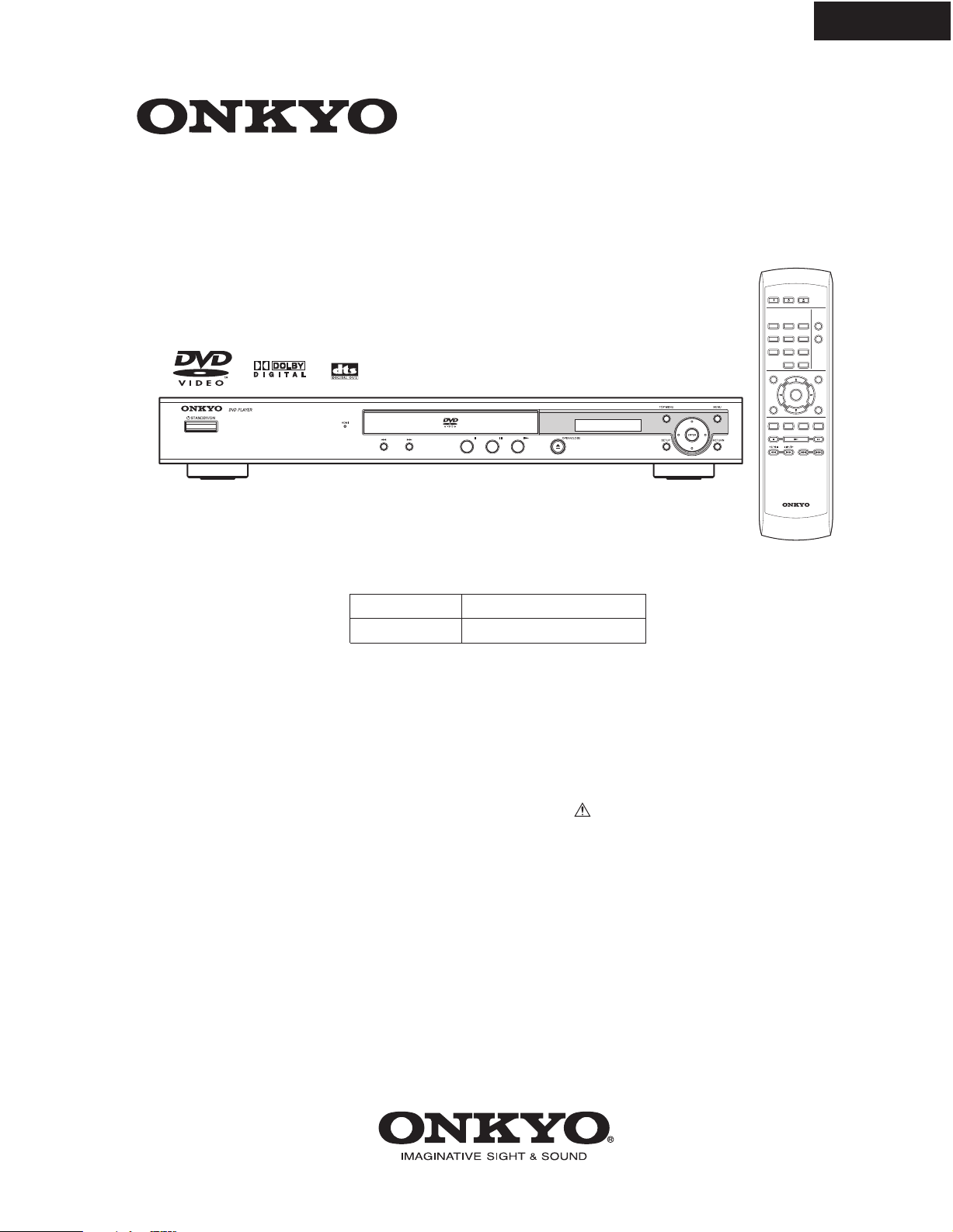
DVD PLAYER
MODEL DV-SP404
(For USA/Canada, Black/ Silver)
DV-SP404
Ref. No. 3947
072006
ON STANDBY
OPEN/
CLOSE
PLAY
MODE
123
DISPLAY
6
45
789
CLEAR
0
ENTER
AUDIO ANGLE SUBTITLE ZOOM
MENU
SETUP
TOP MENU
RETURN
Black and Silver models
BTUA, STUA
BTDD, STDD
110-240V AC, 50/60Hz
120V AC, 60Hz
SAFETY-RELATED COMPONENT
WARNING!!
COMPONENTS IDENTIFIED BY MARK ON THE
SCHEMATIC DIAGRAM AND IN THE PARTS LIST ARE
CRITICAL FOR RISK OF FIRE AND ELECTRIC SHOCK.
REPLACE THESE COMPONENTS WITH ONKYO
PARTS WHOSE PART NUMBERS APPEAR AS SHOWN
IN THIS MANUAL.
MAKE LEAKAGE-CURRENT OR RESISTANCE
MEASUREMENTS TO DETERMINE THAT EXPOSED
PARTS ARE ACCEPTABLY INSULATED FROM THE
SUPPLY CIRCUIT BEFORE RETURNING THE
APPLIANCE TO THE CUSTOMER.
RC-616DV
RC-616DV
Page 2

CAUTION
THIS DIGITAL VIDEO PLAYER EMPLOYS A LASER SYSTEM.
TO ENSURE PROPER USE OF THIS PRODUCT, PLEASE READ THIS SERVICE MANUAL CARE-
FULLY AND RETAIN FOR FUTURE REFERENCE. SHOULD THE UNIT REQUIRE MAINTENANCE,
CONTACT AN AUTHORIZED SERVICE LOCATION-SEE SERVICE PROCEDURE.
USE OF CONTROLS, ADJUSTMENTS OR THE PERFORMANCE OF PROCEDURES OTHER THAN
THOSE SPECIFIED HEREIN MAY RESULT IN HAZARDOUS RADIATION EXPOSURE.
TO PREVENT DIRECT EXPOSURE TO LASER BEAM, DO NOT TRY TO OPEN THE ENCLOSURE.
VISIBLE LASER RADIATION MAY BE PRESENT WHEN THE ENCLOSURE IS OPENED. DO NOT
STARE INTO BEAM.
PREPARATION OF SERVICING
The laser diode used for a pickup head may be destroyed with external static electricity.
Moreover, even if it is operating normally after repair, when static electricity discharge is received at the
time of repair, the life of the product may be shortened.
Please perform the following measure against static electricity, be careful of destruction of a laser diode
at the time of repair.
• Place the unit on a workstation equipped to protect against static electricity, such as conductive mat.
• Soldering iron with ground wire or ceramic type is used.
• A worker needs to use a ground conductive wrist strap for body.
A1-1
Page 3
IMPORTANT SERVICE SAFETY INFORMATION
Safety precautions to be followed during servicing:
1.
Parts marked with an are critical parts for safety. Replace only with the one described in the parts
list.
2.
Before returning the DVD product to the customer, make the appropriate leakage current check or
resistance measurements to ensure that exposed parts are properly insulated from the supply circuit.
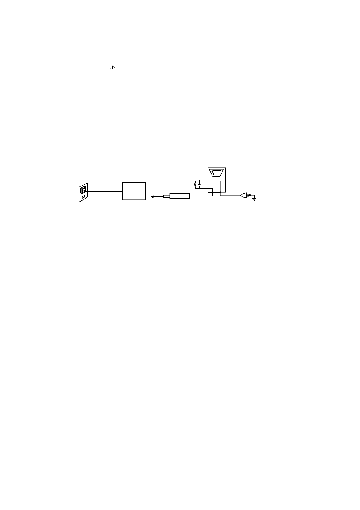
A leakage current check is recommended for this unit. Plug the AC line cord directly into a 120V 60Hz AC
outlet (do not use an isolation transformer for this check). Use a leakage current tester (Fig. 1) or a
metering system which complies with Underwriters Laboratories (UL 1492). Measure for current from all
exposed metal parts of the cabinet to a known earth ground: particularly, any exposed metal part having a
return path to the chassis. Any current measured must not exceed 0.5mA. Any measurement not within
the limits outlined above are indicative of a potential shock hazard and corrective action must be taken
before returning the unit to the customer.
(Reading should not be above 0.5mA)
Leakage Current Tester
PRODUCT UNDER TEST
1.5K ohm
0.15 µF
2-Blade polarized
type cord set
Test all exposed
metal surfaces
TEST PROBE
Fig. 1 AC Leakage Test
KNOWN EARTH
GROUND
A1-2
Page 4

IMPORTANT SAFEGUARDS
1.
READ INSTRUCTIONS
All the safety and operating instructions should be read before the unit is operated.
2.
RET AIN INSTRUCTIONS
The safety and operating instructions should be retained for future reference.
3.
HEED WARNINGS
All warnings on the unit and in the operating instructions should be adhered to.
4.
FOLLOW INSTRUCTIONS
All operating and use instructions should be followed.
5.
CLEANING
Unplug this unit from the wall outlet before cleaning. Do not use liquid cleaners or aerosol cleaners. Use a damp
cloth for cleaning.
6.
A TTACHMENTS
Do not use attachments not recommended by the unit’s manufacturer as they may cause hazards.
7.
WATER AND MOISTURE
Do not use this unit near water. For example, near a bathtub, washbowl, kitchen sink, or laundry tub, in a wet
basement, or near a swimming pool.
8.
ACCESSORIES
Do not place this unit on an unstable cart, stand, tripod, bracket, or table. The
unit may fall, causing serious injury, and serious damage to the unit. Use only
with a cart, stand, tripod, bracket, or table recommended by the manufacturer.
8A.
An appliance and cart combination should be moved with care. Quick stops,
excessive force, and uneven surfaces may cause the appliance and cart
combination to overturn.
9.
VENTILATION
Slots and openings in the cabinet and in the back or bottom are provided for ventilation, to ensure reliable
operation of the unit, and to protect it from overheating. These openings must not be blocked or covered. The
openings should never be blocked by placing the unit on a bed, sofa, rug, or other similar surface. This unit
should never be placed near or over a radiator or heat source. This unit should not be placed in a built-in
installation such as a bookcase or rack unless proper ventilation is provided or the manufacturer’s instructions
have been adhered to.
10.
POWER SOURCES
This unit should be operated only from the type of power source indicated on the rating plate. If you are not sure
of the type of power supply to your home, consult your appliance dealer or local power company . For units
intended to operate from battery power, or other sources, refer to the operating instructions.
11.
GROUNDING OR POLARIZA TION
This unit is equipped with a polarized alternating-current line plug (a plug having one blade wider than the other).
This plug will fit into the power outlet only one way . This is a safety feature. If you are unable to insert the plug
fully into the outlet, try reversing the plug. If the plug should still fail to fit, contact your electrician to replace your
obsolete outlet. Do not defeat the safety purpose of the polarized plug. If your unit is equipped with a 3-wire
grounding-type plug, a plug having a third (grounding) pin, this plug will only fit into a grounding-type power
outlet. This too, is a safety feature. If you are unable to insert the plug into the outlet, contact your electrician to
replace your obsolete outlet. Do not defeat the safety purpose of the grounding-type plug.
12.
POWER-CORD PROTECTION
Power-supply cords should be routed so that they are not likely to be walked on or pinched by items placed upon
or against them, paying particular attention to cords at plugs, convenience receptacles, and the point where they
exit from the appliance.
13.
LIGHTNING
To protect your unit from a lightning storm, or when it is left unattended and unused for long periods of time,
unplug it from the wall outlet and disconnect the antenna or cable system. This will prevent damage to the unit
due to lightning and power line surges.
14.
POWER LINES
An outside antenna system should not be located in the vicinity of overhead power lines or other electric light or
power circuits, or where it can fall into such power lines or circuits. When installing an outside antenna system,
extreme care should be taken to keep from touching such power lines or circuits, as contact with them might be
fatal.
15.
OVERLOADING
Do not overload wall outlets and extension cords, as this can result in a risk of fire or electric shock.
16.
OBJECT AND LIQUID ENTRY
Do not push objects through any openings in this unit, as they may touch dangerous voltage points or short out
parts that could result in fire or electric shock. Never spill or spray any type of liquid into the unit.
PORT ABLE CAR T WARNING
(symbol provided by RETAC)
S3125A
A1-3
Page 5

IMPORTANT SAFEGUARDS (CONTINUED)
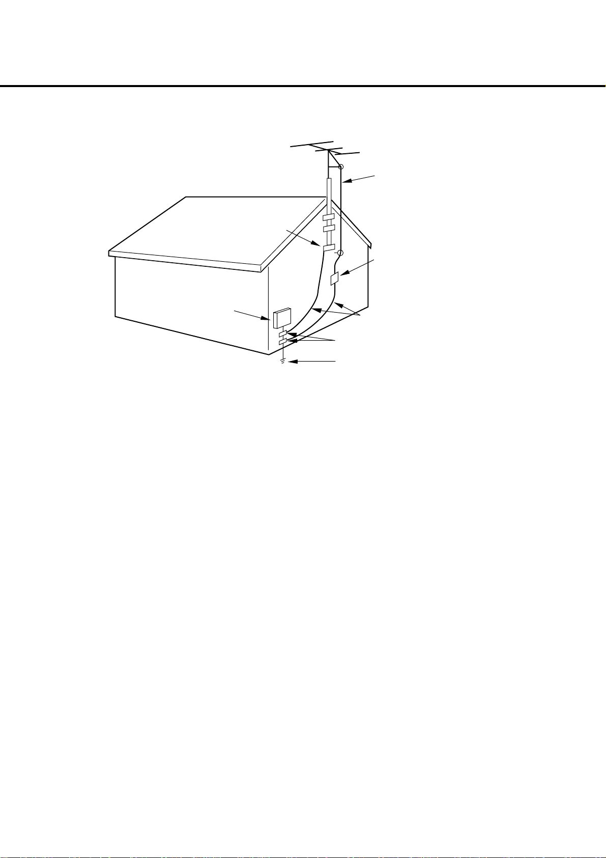
OUTDOOR ANTENNA GROUNDING
17.
If an outside antenna or cable system is connected to the unit, be sure the antenna or cable system is grounded
so as to provide some protection against voltage surges and built-up static charges. Section 810 of the National
Electrical Code, ANSI/NFPA 70, provides information with respect to proper grounding of the mast and supporting
structure, grounding of the lead-in wire to an antenna discharge unit, size of grounding conductors, location of
antenna discharge unit, connection to grounding electrodes, and requirements for the grounding electrode.
SERVICING
18.
Do not attempt to service this unit yourself as opening or removing covers may expose you to dangerous voltage
or other hazards. Refer all servicing to qualified service personnel.
DAMAGE REQUIRING SERVICE
19.
Unplug this unit from the wall outlet and refer servicing to qualified service personnel under the following
conditions:
a.
When the power-supply cord or plug is damaged.
b.
If liquid has been spilled, or objects have fallen into the unit.
c.
If the unit has been exposed to rain or water.
d.
If the unit does not operate normally by following the operating instructions. Adjust only those controls that
are covered by the operating instructions, as an improper adjustment of other controls may result in
damage and will often require extensive work by a qualified technician to restore the unit to its normal
operation.
e.
If the unit has been dropped or the cabinet has been damaged.
f.
When the unit exhibits a distinct change in performance, this indicates a need for service.
REPLACEMENT PARTS
20.
When replacement parts are required, be sure the service technician uses replacement parts specified by the
manufacturer or those that have the same characteristics as the original parts.
Unauthorized substitutions may result in fire, electric shock or other hazards.
SAFETY CHECK
21.
Upon completion of any service or repairs to this unit, ask the service technician to perform safety checks to
determine that the unit is in proper operating condition.
WALL OR CEILING MOUNTING
22.
The product should be mounted to a wall or ceiling only as recommended by the manufacturer.
HEAT
23.
The product should be situated away from heat sources such as radiators, heat registers, stoves, or other
products (including amplifiers) that produce heat.
DISC TRAY
24.
Keep your fingers well clear of the disc tray as it is closing. It may cause serious personal injury.
CONNECTING
25.
When you connect the product to other equipment, turn off the power and unplug all of the equipment from the
wall outlet. Failure to do so may cause an electric shock and serious personal injury. Read the owner's manual of
the other equipment carefully and follow the instructions when making any connections.
SOUND VOLUME
26.
Reduce the volume to the minimum level before you turn on the product. Otherwise, sudden high volume sound
may cause hearing or speaker damage.
SOUND DISTORTION
27.
Do not allow the product output distorted sound for a longtime. It may cause speaker overheating and fire.
HEADPHONES
28.
When you use the headphones, keep the volume at a moderate level. If you use the headphones continuously
with high volume sound, it may cause hearing damage.
LASER BEAM
29.
Do not look into the opening of the disc tray or ventilation opening of the product to see the source of the laser
beam. It may cause sight damage.
DISC
30.
Do not use a cracked, deformed, or repaired disc. These discs are easily broken and may cause serious
personal injury and product malfunction.
NOTE TO CATV SYSTEM INSTALLER
31.
This reminder is provided to call the CATV system installer’s attention to Article 820-40 of the NEC that provides
guidelines for proper grounding and, in particular, specifies that the cable ground shall be connected to the
grounding system of the building, as close to the point of cable entry as practical.
A1-4
Page 6
IMPORTANT SAFEGUARDS (CONTINUED)
EXAMPLE OF ANTENNA GROUNDING AS PER THE NATIONAL ELECTRICAL CODE
ANTENNA LEAD
IN WIRE
GROUND
CLAMP
ANTENNA
DISCHARGE UNIT
(NEC SECTION 810-20)
ELECTRIC SERVICE
EQUIPMENT
GROUNDING CONDUCTORS
(NEC SECTION 810-21)
GROUND CLAMPS
NEC-NATIONAL ELECTRICAL CODE
S2898A
POWER SERVICE GROUNDING
ELECTRODE SYSTEM
(NEC ART 250, PART H)
A1-5
Page 7

DV-SP404 (For USA/CANADA, SILVER)
SERVICE MANUAL
DVD VIDEO PLAYER
This SUPPLEMENT must be used together SERVICE MANUAL for DV-SP404 (For USA/CANADA,
BLACK).
All other test and repair procedures are as shown in the ORIGINAL MANUAL.
Please file this SUPPLEMENT with the ORIGINAL VERSIONS.
SUPPLEMENT
MFR'S VERSION A
Design and specifications are subject to change without notice.
Page 8

MECHANICAL REPLACEMENT PARTS LIST
DV-SP404 (For USA/CANADA, BLACK) DV-SP404 (For USA/CANADA, SILVER)
REF. NO.
101 7A701A785A FRONT CABI ASS'Y 7A701A798A FRONT CABI ASS'Y
101A 701WPBA069 CABINET FRONT 701WPBA073 CABINET FRONT
101B 701WADA004 PANEL FRONT 701WADA005 PANEL FRONT
101C 711WPAA143 PLATE DISPLAY 711WPAA146 PLATE DISPLAY
101D 712WPJC280 FLAP DVD 712WPJC283 FLAP DVD
101F 723656A002 BADGE BRAND 723656A003 BADGE BRAND
101H 737WPAA018 BUTTON CAP 737WPEA020 BUTTON CAP
101I 737WPA0027 BUTTON CAP EJECT 737WPE0033 BUTTON CAP EJECT
101L 738WPJA030 BUTTON FRAME 1 738WPJA035 BUTTON FRAME 1
101N 724000A009 SHEET PC
110 702WSBA071 CABINET TOP 702WSBA070 CABINET TOP
206 8109K3060S SCREW TAP TITE(B) BIND(3D) 3x6 8109K3060U SCREW TAP TITE(B) BIND(3D) 3x6
208 811022680S SCREW TAP TITE(P)BIND 2.6x8 811022680U SCREW TAP TITE(P)BIND 2.6x8
--- 723000D382 CARTON LABEL 723000D388 CARTON LABEL
--- 793WCDD254 GIFT BOX 793WCDD275 GIFT BOX
PART NO. DESCRIPTION PART NO. DESCRIPTION
Page 9
MECHANICAL EXPLODED VIEW
DV-SP404 (For USA/CANADA, SILVER)
101M
101F
208
208
101B
101G
101E
101A
208
101C
101D
101I
101N
101J
101H
101K
101L
101
ADD: 101N
Page 10
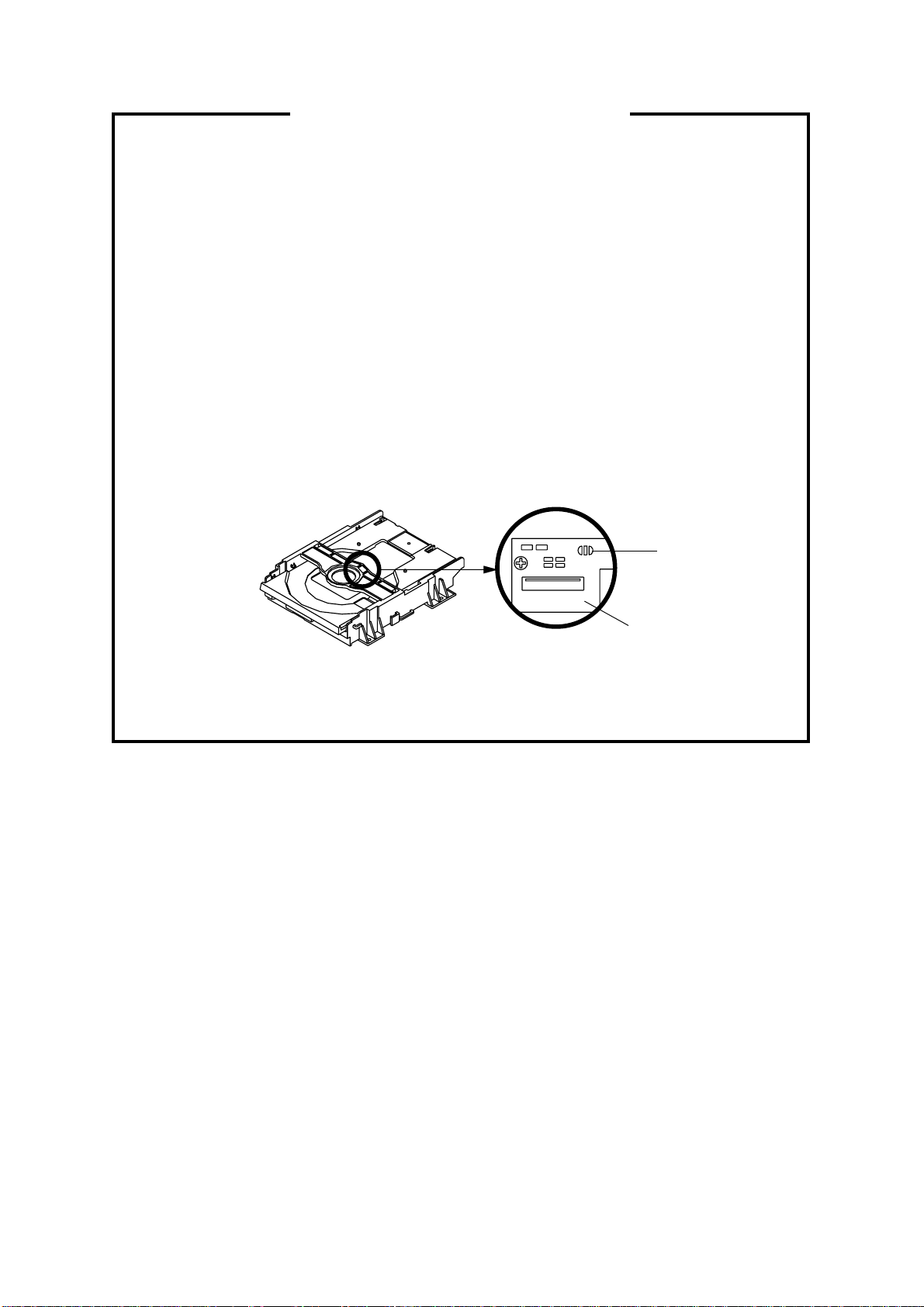
WHEN REPLACING DVD DECK
[ When removing the DVD Deck ]
Before removing Pick Up PCB and DVD PCB connector, the short circuit the position shown in Fig. 1
using a soldering iron. If you remove the DVD Deck with no soldering, the Laser may be damaged.
[ When installing the DVD Deck ]
Remove all the soldering on the short circuit position after the connection of Pick Up PCB and DVD
PCB connector.
NOTE
Before your operation, please read “PREPARATION OF SERVICING”.
•
Use the Lead Free solder.
•
Manual soldering conditions
•
• Soldering temperature: 320 ± 20˚C
• Soldering time: Within 3 seconds
• Soldering combination: Sn-3.0Ag-0.5Cu
When Soldering/Removing of solder, use the draw in equipment over the Pick Up Unit to keep the
•
Flux smoke away from it.
Short circuit using a
soldering iron.
Fig. 1
Pick Up PCB
A1-6
Page 11
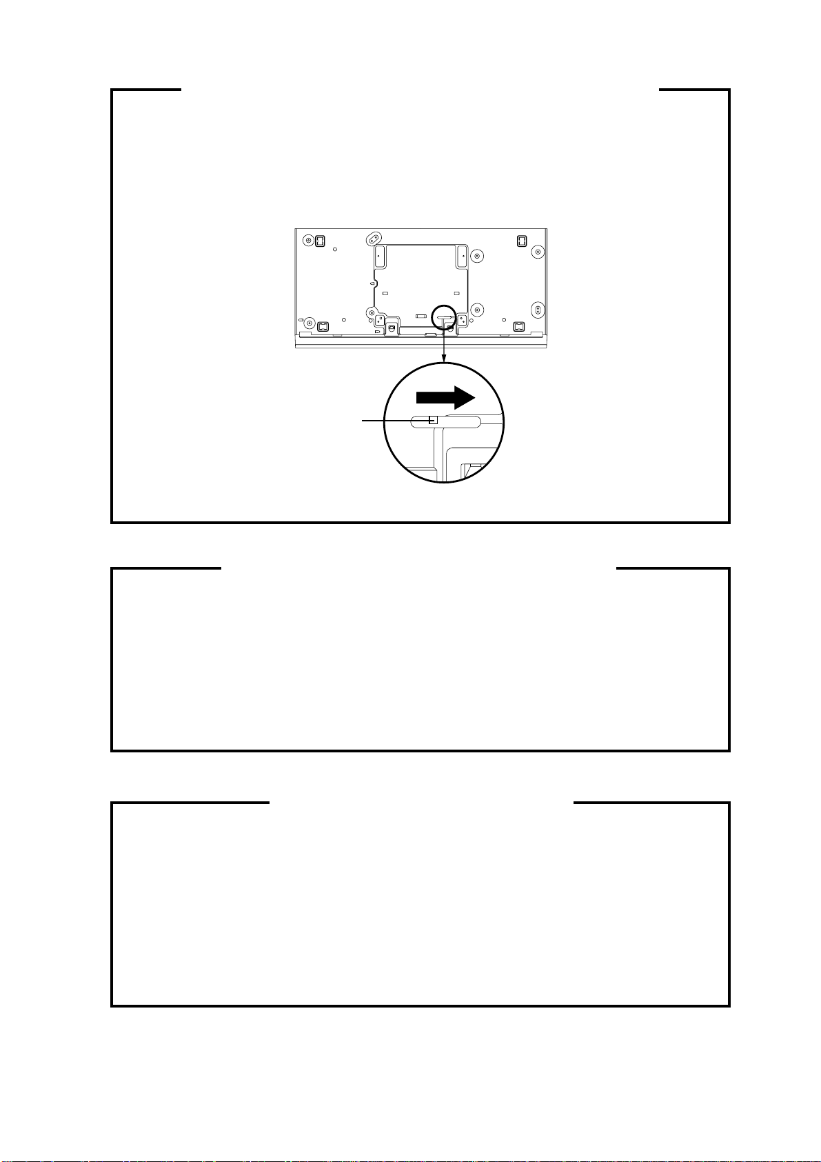
DISC REMOVAL METHOD AT NO POWER SUPPLY
1.
Slide the Rack Loading (White) toward the arrow direction by using a minus driver to release the lock.
(Refer to Fig. 1)
2.
Manually open the Tray.
NOTE:
Please strongly pushing Rack Loading (White) to release the lock because the tray doesn't go out
easily.
DVD Player (Bottom Side)
Rack Loading (White)
Fig. 1
PARENTAL CONTROL - RATING LEVEL
4 DIGIT PASSWORD CANCELLATION
If the stored 4 digit password in the Rating Level menu needs to be cancelled, please follow the steps
below.
Set the DVD to the Stand-by Mode.
1.
Press and hold the 'STOP' key on the front panel.
2.
Simultaneously press and hold the POWER key on the front panel.
3.
The 4 digit password has now been cleared.
4.
NOTE: The above procedure will reset ALL of the player's settings to the default factory state.
PREPARATION OF SERVICING
The laser diode used for a pickup head may be destroyed with external static electricity.
Moreover, even if it is operating normally after repair, when static electricity discharge is
received at the time of repair, the life of the product may be shortened.
Please perform the following measure against static electricity, be careful of destruction of a
laser diode at the time of repair.
• Place the unit on a workstation equipped to protect against static electricity, such as
conductive mat.
• Soldering iron with ground wire or ceramic type is used.
• A worker needs to use a ground conductive wrist strap for body.
A1-7
Page 12

ABOUT LEAD FREE SOLDER (PbF)
Distinction of PbF PCB:
PCBs (manufactured) using lead free solder will have a PbF printing on the PCB.
(Please refer to figures.)
Caution:
Pb free solder has a higher melting point than standard solder;
•
Typically the melting point is 86°F~104°F(30°C~40°C) higher.
Please use a soldering iron with temperature control and adjust it to 650°F ± 20°F (350°C ± 10°C).
In case of using high temperature soldering iron, please be careful not to heat too long.
Pb free solder will tend to splash when heated too high (about 1100°F/ 600°C).
•
All products with the printed circuit board with PbF printing must be serviced with lead free solder.
•
When soldering or unsoldering, completely remove all of the solder from the pins or solder area,
and be sure to heat the soldering points with the lead free solder until it melts sufficiently.
Recommendations
Recommended lead free solder composition is Sn-3.0Ag-0.5Cu.
A1-8
Page 13

TABLE OF CONTENTS
CAUTION .............................................................................................................................................................
IMPORTANT SERVICE SAFETY INFORMATION .............................................................................................
IMPORTANT SAFEGUARDS..............................................................................................................................
WHEN REPLACING DVD DECK ........................................................................................................................
DISC REMOVAL METHOD AT NO POWER SUPPLY........................................................................................
PARENTAL CONTROL- RATING LEVEL ..........................................................................................................
PREPARATION OF SERVICING ........................................................................................................................
ABOUT LEAD FREE SOLDER (PbF).................................................................................................................
TABLE OF CONTENTS.......................................................................................................................................
GENERAL SPECIFICATIONS ............................................................................................................................
DISASSEMBLY INSTRUCTIONS
1.REMOVAL OF MECHANICAL PARTS AND P.C. BOARDS .........................................................................
2.REMOVAL OF DVD DECK PARTS ...............................................................................................................
3.REMOVAL AND INSTALLATION OF FLAT PACKAGE IC ...........................................................................
SERVICING FIXTURES AND TOOLS ................................................................................................................
RE-WRITE FOR DVD FIRMWARE .....................................................................................................................
TROUBLESHOOTING GUIDE ............................................................................................................................
BLOCK DIAGRAMS
DVD LOADER/MPEG .......................................................................................................................................
POWER ............................................................................................................................................................
OVERALL BLOCK DIAGRAM .............................................................................................................................
PRINTED CIRCUIT BOARDS
DVD MT ............................................................................................................................................................
POWER/OPERATION/OPERATION 2/OPERATION 3/OPERATION 4 ...........................................................
LOADING MOTOR/SW .....................................................................................................................................
SCHEMATIC DIAGRAMS
MPEG/MICON/DSP ..........................................................................................................................................
MEMORY ..........................................................................................................................................................
LOADER/MOTOR DRIVE .................................................................................................................................
AUDIO JACK.....................................................................................................................................................
VIDEO JACK .....................................................................................................................................................
HDMI .................................................................................................................................................................
POWER PORT..................................................................................................................................................
POWER.............................................................................................................................................................
DISPLAY ...........................................................................................................................................................
LOADING MOTOR/SW .....................................................................................................................................
INTERCONNECTION DIAGRAM .........................................................................................................................
WAVEFORMS ......................................................................................................................................................
MECHANICAL EXPLODED VIEW .......................................................................................................................
DVD DECK EXPLODED VIEW ............................................................................................................................
MECHANICAL REPLACEMENT PARTS LIST ...................................................................................................
DVD DECK REPLACEMENT PARTS LIST .........................................................................................................
ELECTRICAL REPLACEMENT PARTS LIST .....................................................................................................
A1-1
A1-2
A1-3~A1-5
A1-6
A1-7
A1-7
A1-7
A1-8
A2-1
A3-1~A3-5
B1-1
B2-1~ B2-4
B3-1, B3-2
C-1
C-1
D-1~D-6
E-1, E-2
E-3, E-4
E-5, E-6
F-1, F-2
F-3, F-4
F-5, F-6
G-1, G-2
G-3, G-4
G-5, G-6
G-7, G-8
G-9, G-10
G-11, G-12
G-13, G-14
G-15, G-16
G-17, G-18
G-19, G-20
G-21, G-22
H-1
I1-1, I1-2
I2-1
J1-1
J2-1
J3-1~J3-4
A2-1
Page 14
GENERAL SPECIFICATIONS
G-1 DVD System Color System NTSC
Disc
Disc Diameter 120 mm , 80 mm
Drive DM4PB
Search speed Fwd 4 step
Fwd-Actual 4, 8, 16, 32 times
Rev 4 step
Rev-Actual 4, 8, 16, 32 times
Slow speed Fwd 4 step
Fwd-Actual 1/16, 1/8, 1/4, 1/2 times
Rev 4 step
Rev-Actual 1/16, 1/8, 1/4, 1/2 times
Zoom Zoom 2 step
Zoom-Actual 2, 4 times
G-2 Power Power Source AC 120V 60Hz
DC --
Power Consumption 7 W
Stand by 0.9 W
Per Year -- W
Energy Star No
Protector Power Fuse Yes
Safety Circuit Yes
IC Protector (Micro Fuse) No
G-3 Regulation Safety UL/CSA(C-UL)
Radiation FCC/IC
Laser DHHS
G-4 Temperature Operation 5 oC - 40 oC
Storage -20 oC - 60 oC
G-5 Operating Humidity Less than 80% RH
G-6 Signal Video Signal Output Level 1 V p-p / 75 ohm
S/N Ratio (Weighted) 65 dB
Horizontal Resolution at DVD 500 Lines
RGB Signal Output Level -Component Video Output Level (Y) 1.0V p-p / 75 ohm
Output Level (Cb, Cr) 0.7V p-p / 75 ohm
Audio Signal Input Level Microphone --- dBm / --- ohm
Output Level Line
S/N Ratio at (Weighted) 90dB
Harmonic Distortion : 0.0065% (1KHz)
Frequency Response : at DVD 4 Hz - 44 KHz (96KHz)
Frequency Response : at SVCD 4 Hz - 20 KHz
Frequency Response : at VIDEO CD 4 Hz - 20 KHz
Frequency Response : at CD 4 Hz - 20 KHz
Frequency Response : at DVD Audio --
Frequency Response : at SACD -Digital Audio Signal Output Level
G-7 OSD Language English/French/Spanish/German/Italian
DVD, CD-DA, CD-R/RW, Video CD, SVCD
DVD-R/RW, DVD+R/+RW (w/o VCPS)
-12 dBm/ 1k ohm (-20dBFs, 0dBFs=2.0Vrms)
0.5 V p-p / 75 ohm
A3-1
Page 15

GENERAL SPECIFICATIONS
G-8
Remote Control Unit
Unit RC-LP
Glow in Dark Remocon No
Remocon Format ONKYO
Format NEC
Custom Code D2-2B
Power Source Voltage (D.C) 3V
UM size x pcs UM-3 x 2 pcs
Total Keys 36 Keys
Power ON Yes
Power Off (STAND BY) Yes
Open/Close Yes
Audio Yes
Subtitle Yes
Angle Yes
1 Yes
2 Yes
3 Yes
4 Yes
5 Yes
6 Yes
7 Yes
8 Yes
9 Yes
0 Yes
Clear Yes
Enter Yes
Top Menu Yes
Menu Yes
Set up (Home Menu) Yes
Return Yes
Up Yes
Down Yes
Right Yes
Left Yes
Enter No
<< (Scan/Slow/Step) Yes
>> (Scan/Slow/Step) Yes
Play Yes
|<< (Search) Yes
>>| (Search) Yes
Pause Yes
Stop Yes
Play Mode Yes
Surround No
Zoom Yes
Display Yes
Key Control b No
Key Control # No
A3-2
Page 16

GENERAL SPECIFICATIONS
G-9
G-10
DVD Features
Accessories
Progressive Video Out Yes
Echo No
Mic Mixing No
Digital Out (Dolby Digital) Yes
(MPEG) Yes
(PCM) Yes
(DTS) Yes
Down Mix Out (Dolby Digital) Yes
(DTS) No
(SACD) No
(DVD Audio) No
Surround MTK original Surround
Screen Saver Yes
Auto Stop No
BNR No
Dynamic Range Control Yes
Disc Navigator Yes
Video CD Playback Yes
SVCD Playback Yes
SACD Playback No
DVD Audio Playback No
DivX Playback Yes
DMF Support No
VR Format Playback Yes
Fujicolor CD Yes
KODAK Picture CD Yes
MP3 Playback Yes
WMA Playback Yes
JPEG Playback Yes
Audio DAC 96kHz / 24bit
Auto Power Off Yes
Closed Caption signal in VBI (DVD Playback)
Owner's Manual Language English
w/Guarantee Card No
Remote Control Unit Yes
Guarantee Card Yes
Warning Sheet No
Service Station List No
Important Tag No
AC Plug Adapter No
Quick Set-up Sheet No
Battery Yes
UM size x pcs UM-3 x 2 pcs
OEM Brand No
AC Cord No
AV Cord Yes (1.2m)
1Pin RCA Cable Yes (1.2m)
HDMI Cable No
S-Video Cable No
21pin Cable (Double Shield) No
800 No Sticker No
Toll Free Insert Sheet No
Safety Tip No
Security Tag No
Sheet Information (Return) No
Registration Card No
Netflix Sheet No
Helpline Sheet No
Helpline Sticker No
Information Sheet No
Yes
A3-3
Page 17

GENERAL SPECIFICATIONS
G-11 Interface Switch-Front Standby/On Yes
Play Yes
Open/Close Yes
Skip (>>|) Yes
Skip (|<<) Yes
Pause Yes
Stop Yes
Top Menu Yes
Home Menu Yes
Menu Yes
Return Yes
Enter Yes
Up Yes
Down Yes
Right Yes
Left Yes
Shuttle (Search/REV/FWD) No
Main Power SW No
Display Yes
DISPLAY Type Fluorescent Indicator
Pause/Play Yes
Progressive Yes
DVD No
Remain Yes
Surround No
Track No
A No
-B No
Video No
CD No
All No
PROG No
Mic Mark No
Title Yes
Repeat Yes
Angle Yes
Chapter Yes
Music Calendar (1-14, Play) No
7-seg Digit (8) Yes
Terminals-Front Mic In No
Volume Control No
Echo Control No
Terminals-Rear Video Output RCA x 1
S-Video Output S-Jack x1
Component Video Output RCA x3 (Y, Cr, Cb)
D1 No
Audio Output RCA x 2 (Stereo)
Euro Scart No
Digital Audio Output RCA x 1 (Digital Audio)
5.1ch Audio Output No
HDMI Output Yes
AC Inlet No
Indicator HDMI Yes(Red)
G-12 Set Size Dimensions (Approx.) W x D x H (mm) 435 x 208 x 60.5
G-13 Weight Net (Approx.) 1.9kg ( 4.2 lbs)
Gross (Approx.) 2.8kg ( 6.2 lbs)
A3-4
Page 18

GENERAL SPECIFICATIONS
G-14 Carton Master Carton No
Content --- Sets
Material --- / ---
Dimensions W x D x H (mm) ---
Description of Origin --Gift Box Material Single/Brown
W/Color Photo Label No
Dimensions W x D x H (mm) 507 x 290 x 130
Description of Origin Yes
Natural Dropping At 1 Corner / 3 Edges /
6 Surface
Green procurement of Pioneer
G-15
G-16
Cabinet Material
Environment
Drop Test
Height (cm) 80cm
Container Stuffing 3,220 Sets/40' container
Cabinet Front PS 94V2 or More / NON DECABROM
PCB Non-Halogen Demand No
Eyelet Demand No
Environmental standard requirement (by buyer)
WEEE No
Pb-free Phase3 (Phase3A)
Measures for Whisker Yes
A3-5
Page 19
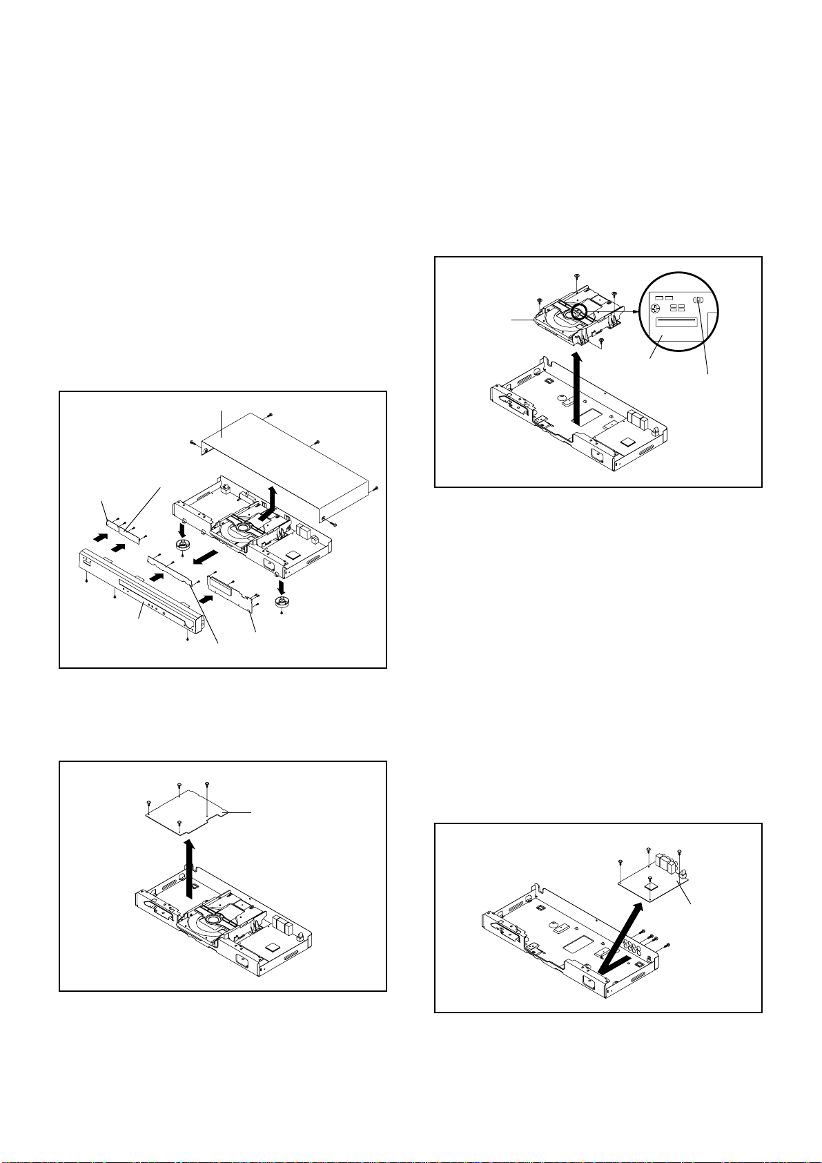
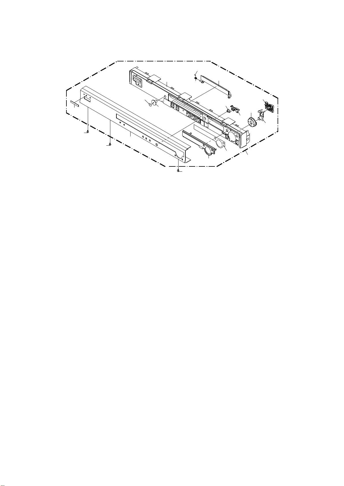
DISASSEMBLY INSTRUCTIONS
1. REMOVAL OF MECHANICAL PARTS
AND P.C. BOARDS
1-1:
TOP CABINET/FRONT CABINET/OPERATION 1/2/
3/4 PCB (Refer to Fig. 1-1)
1.
Remove the 5 screws 1.
2.
Remove the Top Cabinet in the direction of arrow (A).
3.
Remove the 2 screws 2.
4.
Remove the Leg in the direction of arrow (B).
5.
Remove the 3 screws 3.
6.
Disconnect the following connector: (CP4002).
7.
Unlock the 2 supports 4.
8.
Remove the Front Cabinet in the direction of arrow (C).
9.
Remove the 10 screws 5.
10.
Remove the 2 screws 6.
11.
Remove the Operation 1/2/3/4 PCB in the direction of
arrow (C).
Top Cabinet
1
(D)
Operation 4 PCB
6
5
5
5
(D)
3
Front Cabinet
(B)
5
(C)
5
2
5
5
(D)
(D)
4
3
Operation 2 PCB
Operation 3 PCB
4
3
1-2: POWER PCB (Refer to Fig. 1-2)
1.
Disconnect the following connector: (CP502).
2.
Remove the 4 screws 1.
3.
Remove the Power PCB in the direction of arrow.
1
1
1
1
1
(A)
5
5
6
5
2
Operation 1 PCB
Power PCB
1
1
(B)
Fig. 1-1
1-3: DVD DECK (Refer to Fig. 1-3)
1.
Short circuit the position shown in Fig. 1-3 using a
soldering iron. If you remove the DVD Deck with no
soldering, the Laser may be damaged.
2.
Disconnect the following connectors:
(CP2301, CP2302, CP2303).
3.
Remove the 4 screws 1.
4.
Remove the DVD Deck in the direction of arrow.
1
1
DVD Deck
1
1
1
Pick Up PCB
Short circuit using a
soldering iron.
Fig. 1-3
NOTE
Before your operation, please read “PREPARATION
1.
OF SERVICING”.
Use the Lead Free solder.
2.
Manual soldering conditions
3.
• Soldering temperature: 320 ± 20˚C
• Soldering time: Within 3 seconds
• Soldering combination: Sn-3.0Ag-0.5Cu
When Soldering/Removing of solder, use the drawing
4.
equipment over the Pick Up Unit to prevent the Flux
smoke from it.
When installing the DVD Deck, remove all the soldering
5.
on the short circuit position after the connection of Pick
Up PCB and DVD MT PCB connector.
1-4: DVD MT PCB (Refer to Fig. 1-4)
1.
Remove the 3 screws 1.
2.
Remove the screw 2.
3.
Remove the 4 screws 3.
4.
Remove the DVD MT PCB in the direction of arrow.
Fig. 1-2
B1-1
3
1
3
1
1
3
DVD MT PCB
2
3
Fig. 1-4
Page 20

DISASSEMBLY INSTRUCTIONS
2. REMOVAL OF DVD DECK PARTS
NOTE
1. Disassemble only the DVD DECK PARTS parts listed
here. Minute adjustments are needed if the
disassembly is done. If the repair is needed except
listed parts, replace the DVD MECHA ASS'Y.
2-1: TRAY (Refer to Fig. 2-1-A)
Set the Tray opened. (Refer to the DISC REMOVAL
1.
METHOD AT NO POWER SUPPLY)
Unlock the 2 supports 1 and draw it while sagging the
2.
Tray.
Loader Ass'y
Push to Sag
Tray
NOTE
In case of the Tray installation, install them as the circled
1.
section of Fig. 2-1-B so that the each markers are met.
1
1
Push to Sag
Fig. 2-1-A
NOTE
In case of the Traverse Ass'y, install it from (1) to (4) in
1.
order. (Refer to Fig. 2-2-B)
In case of the Traverse Ass'y installation, hook the wire
2.
on the Loader Ass'y as shown Fig. 2-2-C.
Loader Ass'y (Bottom Side)
(3)
(3)
(3)
(2)
(4)
Check Lock
(4)
Loader Ass'y
(3)
(1)
Rack Loading
Holder Traverse
Traverse Ass'y
Fig. 2-2-B
Loader Ass'y
Tray
Fig. 2-1-B
2-2: TRAVERSE ASS'Y (Refer to Fig. 2-2-A)
Remove the screw 1.
1.
Unlock the 2 supports 2.
2.
Remove the Insulator (R) from the Loader Sub Ass'y.
3.
Remove the Traverse Ass'y.
4.
1
2
2
Loader Sub Ass'y
Insulator (R)
Traverse Ass'y
• Screw Torque: 2.0 ± 0.3kgf•cm
Fig. 2-2-A
Check Hook
Fig. 2-2-C
2-3: LOADING MOTOR PCB ASS'Y/ LOADING BELT
(Refer to Fig. 2-3-A)
1.
Remove the Loading Belt.
2.
Remove the screw 1.
3.
Remove the Loading Motor PCB Ass'y.
4.
Remove the 2 screws 2.
5.
Remove the Loading Motor.
6.
Remove the Gear Pulley.
Loading Belt
• Screw Torque: 2.5 ± 0.3kgf•cm (Screw 1)
• Screw Torque: 1.0 ± 0.3kgf•cm (Screw 2)
2
2
Gear Pulley
Loading Motor
Loading Motor PCB Ass’y
1
Loader Sub Ass'y
Fig. 2-3-A
B2-1
Page 21

DISASSEMBLY INSTRUCTIONS
NOTE
1.
In case of the Pulley Motor installation, check if the value
of the Fig. 2-3-B is correct.
2.
When installing the wire of the Loading Motor PCB Ass'y,
install it correctly as Fig. 2-3-C.
Manual soldering conditions
• Soldering temperature: 320 ± 20˚C
• Soldering time: Within 3 seconds
• Soldering combination: Sn-3.0Ag-0.5Cu
3.
When installing the Loading Motor PCB Ass'y, install it
correctly as Fig. 2-3-D.
4.
In case of the Loading Motor PCB Ass'y installation, hook
the wire on the Loader Sub Ass'y as shown Fig. 2-3-E.
Pulley Motor
Loading Motor
Safety surface for pressing
of the insert.
BROWN (1)
WHITE (2)
• Install wire from (1) to (2) in order.
7.0 ± 0.1mm
Fig. 2-3-B
2-4: RACK LOADING/MAIN GEAR/PULLEY GEAR
(Refer to Fig. 2-4-A)
1.
Unlock the support 2 and remove the Gear Pulley.
2.
Remove the Gear Main.
3.
Press down the catcher 1 and slide the Rack Loading.
Gear Pulley
Gear Main
2
1
Rack Loading
Loader Sub Ass’y
Fig. 2-4-A
NOTE
1.2.In case of the Rack Loading installation, hook the Rack
Loading on the Loader Sub Ass'y as shown Fig. 2-4-B.
When installing the Gear Main, take care the direction
of up or down as shown Fig. 2-4-C.
Rack Loading
Rack Loading
Check Hook
Loading Motor PCB Ass’y
AB
The Lever should be position
between A and B.
Check Hook
Fig. 2-3-C
Fig. 2-3-D
Loader Sub Ass'y (Bottom Side)
Check Hook
Fig. 2-4-B
Up Side
Main Gear
Down Side
Fig. 2-4-C
2-5: CLAMPER ASS'Y (Refer to Fig. 2-5-A)
Press the Clamper and rotate the Plate Clamper clockwise,
1.
then unlock the 3 supports 1.
Remove the Plate Clamper, Magnet Clamper and Clamper.
2.
Plate Clamper
Magnet Clamper
Main Frame
Check Hook
Loading Motor PCB Ass’y
Fig. 2-3-E
B2-2
1
1
Clamper
1
Fig. 2-5-A
Page 22

DISASSEMBLY INSTRUCTIONS
NOTE
1. In case of the Clamper Ass'y installation, install
correctly as Fig. 2-5-B.
Feed Motor
Gear Motor
Plate Clamper
Clamper
Check Lock
Fig. 2-5-B
2-6:
HOLDER TRAVERSE/INSULATOR (F)/INSULATOR
(R) (Refer to Fig. 2-6-A)
Remove the Holder Traverse.
1.
Remove the 2 Insulator (F).
2.
Remove the Insulator (R).
3.
Insulator (R)
Traverse Ass'y
Insulator (F)
Holder Traverse
Insulator (F)
Fig. 2-6-A
NOTE
1. In case of the Insulator (F) installation, install correctly
as Fig. 2-6-B.
Insulator (F)
5
Traverse Ass'y
Rack Feed Ass'y
• Screw Torque: 1.3 ± 0.3kgf•cm (Screw 2)
• Screw Torque: 3.0 ± 0.3kgf•cm (Screw 3)
• Screw Torque: 1.0 ± 0.3kgf•cm (Screw 4, 5)
1
5
Gear Feed
4
Gear Middle
2
Switch PCB Ass'y
3
Fig. 2-7-A
NOTE
1.
When installing the Rack Feed Ass'y, push both ends to
align the teeth as shown Fig. 2-7-B. Then install it.
2.
In case of the Gear Motor installation, check if the value
of the Fig. 2-7-C is correct.
3.
When installing the wire of the Switch PCB Ass'y, install
it correctly as Fig. 2-7-D.
Manual soldering conditions
• Soldering temperature: 320 ± 20˚C
• Soldering time: Within 3 seconds
• Soldering combination: Sn-3.0Ag-0.5Cu
4.
After the assembly of the Traverse Ass'y, hook the wire
on the Traverse Ass'y as shown Fig. 2-7-E.
Rack Feed Ass'y
Traverse Holder
Fig. 2-6-B
2-7:
SWITCH PCB ASS'Y/GEAR MIDDLE/GEAR FEED/RACK
FEED ASS'Y/FEED MOTOR (Refer to Fig. 2-7-A)
Unlock the support 1.
1.
Remove the Gear Middle.
2.
Remove the screw 2.
3.
Remove the Rack Feed Ass'y.
4.
Remove the screw 3.
5.
Remove the Switch PCB Ass'y.
6.
Remove the screw 4.
7.
Remove the Gear Feed.
8.
Remove the 2 screws 5.
9.
Remove the Feed Motor.
10.
Remove the Gear Motor.
11.
B2-3
Push
Gear Motor
Feed Motor
[OK] [NG]
Safety surface for pressing
of the insert.
Push
Fig. 2-7-B
8.0 ± 0.2mm
Fig. 2-7-C
Page 23

DISASSEMBLY INSTRUCTIONS
Switch PCB Ass'y
~ SPINDLE MOTOR ~
Check Hook
Check Hook
• Loosen the wire in the direction of the arrow.
YELLOW (2)
GREEN (1)
Traverse Ass'y
Check Hook
Check Hook
2-8: FFC WIRE HANDLING
~ FEED MOTOR ~
WHITE (4)
BROWN (3)
• Install wire from (1) to (4) in order.
Fig. 2-7-D
Fig. 2-7-E
1.
When installing the FFC, fold it correctly and install it as
shown from Fig. 2-8.
NOTE
Do not make the folding lines except the specified
1.
positions for the FFC.
[ 24 pin FFC ]
Printing Surface
79 ± 1mm
Fold
Reinforcement Plate
To Pick Up PCB
Fig. 2-8
B2-4
Page 24

DISASSEMBLY INSTRUCTIONS
3.
REMOVAL AND INSTALLATION OF
FLAT PACKAGE IC
REMOVAL
Put Masking Tape (cotton tape) around the Flat Pack-
1.
age IC to protect other parts from any damage.
(Refer to Fig. 3-1.)
NOTE
Masking is carried out on all the parts located within
10 mm distance from IC leads.
When IC starts moving back and forth easily after
3.
desoldering completely, pickup the corner of the IC using
a tweezers and remove the IC by moving with the IC
desoldering machine. (Refer to Fig. 3-3.)
NOTE
Some ICs on the PCB are affixed with glue, so be
careful not to break or damage the foil of each IC
leads or solder lands under the IC when removing it.
Blower type IC
desoldering
machine
Masking Tape
(Cotton Tape)
Heat the IC leads using a blower type IC desoldering
2.
IC
machine. (Refer to Fig. 3-2.)
NOTE
Do not rotate or move the IC back and forth , until IC
can move back and forth easily after desoldering the
leads completely.
Blower type IC
desoldering machine
Fig. 3-1
Tweezers
IC
Peel off the Masking Tape.4.
Absorb the solder left on the pattern using the Braided
5.
Shield Wire. (Refer to Fig. 3-4.)
NOTE
Do not move the Braided Shield Wire in the vertical
direction towards the IC pattern.
Fig. 3-3
Braided Shield Wire
Soldering Iron
IC
Fig. 3-2
IC pattern
Fig. 3-4
B3-1
Page 25

DISASSEMBLY INSTRUCTIONS
INSTALLATION
Take care of the polarity of new IC and then install the
1.
new IC fitting on the printed circuit pattern. Then solder
each lead on the diagonal positions of IC temporarily.
(Refer to Fig. 3-5.)
Soldering Iron
Solder temporarily
Supply the solder from the upper position of IC leads
2.
Solder temporarily
sliding to the lower position of the IC leads.
(Refer to Fig. 3-6.)
Fig. 3-5
When bridge-soldering between terminals and/or the
4.
soldering amount are not enough, resolder using a Thintip Soldering Iron. (Refer to Fig. 3-8.)
Thin-tip Soldering Iron
IC
Fig. 3-8
Finally, confirm the soldering status on four sides of the
5.
IC using a magnifying glass.
Confirm that no abnormality is found on the soldering
position and installation position of the parts around the
IC. If some abnormality is found, correct by resoldering.
NOTE
When the IC leads are bent during soldering and/or
repairing, do not repair the bending of leads. If the
bending of leads are repaired, the pattern may be
damaged. So, always be sure to replace the IC in this
case.
Soldering IronSolder
IC
Absorb the solder left on the lead using the Braided
3.
Supply soldering
from upper position
to lower position
Shield Wire. (Refer to Fig. 3-7.)
NOTE
Do not absorb the solder to excess.
Soldering Iron
IC
Braided Shield Wire
Fig. 3-6
Fig. 3-7
B3-2
Page 26

SERVICING FIXTURES AND TOOLS
Remote control JIG
Ref. No.
–––
Part No.
–––
JG176 Up-Date Disc
Parts Name
Remote control JIG
Check for the Firmware version
Up-Date of the Firmware
JG176
APJG176112
Up-Date Disc
Up-Date of the Firmware
RE-WRITE FOR DVD FIRMWARE
Turn on the power.
1.
Open the DVD tray.
2.
Place the Up-Date Disc and close the tray. (Refer to SERVICING FIXTURE AND TOOLS)
3.
The reading will start and the Fig. 1 screen will appear.
Upgrade File DETECTED
Upgrade?
Press Play To Start
Remarks
Fig. 1
Press the PLAY key on the set.
4.
The data reading will start.
And, "File Copying" appears on the TV monitor.
After the finishing of the data reading, tray will open automatically.
The display will change to “CLEAR”.
Remove the Up-Date Disc.
5.
CHECK FOR THE FIRMWARE VERSION
6.
Turn on the power, then press "CHECK SUM" key on the remote control JIG for more than 1 second.
Firmware version will be displayed on the screen.
When the changed version displays, the Re-write will be completed.
REAGION: 1
Y E B 6 4 2 0 A
Fixed
Released times on the same date
Release date (Example: 2006.4.20)
A = October
ROM NUMBER
REG CHK
SUM CHK
FL VERSION
CHIP VERSION
AREA: WY
YEB6420A
10
02A5
1.16
1389FE
Fig. 2
B = November
Turn off the power
7.
C = December
C-1
Page 27

POWER DOES NOT TURN ON
TROUBLESHOOTING GUIDE
Is the voltage at pin 8 and
pin 9 of CP502 about
3.3V and at pin 5 of
CP502 about 5V?
Yes
Is there waveform at
X4001 about 3.0Vp-p ?
Yes
Write DVD FIRMWARE DATA.
No
No
Check AT+3.3V line of POWER BLOCK.
Check Q515 and peripheral circuit.
Check X4001, IC4001 and
peripheral circuit.
D-1
Page 28

DECK DOES NOT ACCEPT
OPEN/CLOSE
TROUBLESHOOTING GUIDE
Is the voltage at pins 3,18 and
19 of IC2301 about DC6V ?
Yes
Is the lose connection
at CP2302 to DECK ?
No
Change DVD LOADER.
No
Yes
Check P.CON 6V line of
POWER BLOCK.
Check CP2302
connection to DECK.
D-2
Page 29

TROUBLESHOOTING GUIDE
DOES NOT LIGHT ON DISPLAY
Is the voltage at pin 13
and pin 43 of IC651
about 3V ?
Yes
Replace V651 or IC651.
No
Check AT+3.3V line of
POWER BLOCK.
D-3
Page 30

NO PLAYBACK PICTURE OF AV
JACK
TROUBLESHOOTING GUIDE
Is there a voltage
(beam current) at
JG008 and JG009 ?
Yes
Is there a signal at
pin 164 of IC4001 ?
Yes
Is there video signal at
pin 33 of IC7301 ?
No
Change IC7301.
No
No
Yes
Check LOADER BLOCK.
Check IC4001 and
peripheral circuit.
Check J7302 and peripheral
circuit.
D-4
Page 31

NO DIGITAL AUDIO ON
PLAYBACK OF COAXIAL JACK
TROUBLESHOOTING GUIDE
Is there waveform at pin 7
of J7301 about 0.3Vp-p?
No
Is there waveform at
pin 159 of IC4001
about 0.3Vp-p ?
No
Change IC4001.
Yes
Yes
Check connection at RCA
Cable.
Check Q8005 and
peripheral circuit.
D-5
Page 32

NO ANALOG AUDIO ON
PLAYBACK
TROUBLESHOOTING GUIDE
Is there AUDIO signal
at pins 1 and 7 of
IC8003 ?
No
Is there AUDIO signal at
pins 2 and 6 of IC8003 ?
No
Change IC8003.
Yes
Yes
Check J8003 and peripheral
circuit.
Check AT pins 184 and
186 of IC4001.
D-6
Page 33

DVD LOADER/MPEG BLOCK DIAGRAM
DVD
Loader
(DM-4)
OPU
SPINDLE/
STEPING/
SLED
MOTOR
C
IOA, V20
RF, A, B, C, D, E, F, MDI1
LD_DVD, LD_CD
T+/-, F+/-,
LOAD+/-,
MOT_SLED+/-,
MOT_SPDL+/-
A
Q2302~2305
LD DRIVE
D
MOTOR DRIVER IC
IC2301
LA6565VR-TLM-E
LIMIT, TRIN, TROUT,
OPO, OP+/-
A0~A20, AD0~AD7,
PRD#, PCE#, PWR#
MA0~MA11, DQ0~DQ15,
DQM0, DQM1, DBA0, DBA1,
SDCLK, SDCKE, DWE#,
DRAS#, DCAS#, DCS#
LDO1, LDO2
DMSO, FMSO,
TROPEN, TRCLOSE,
TRSO, FOSO,
STBY, V1P4
X4001
27MHz
MPEG/MICON IC
IC4001
MT1389FE/E-L
RESET
LETTER, SQUEEZE, VSEL1,
I/XP, R/CR, B/CB, G/Y, C/V
A, B
AUDIO L, R
RESET IC
IC4003
BD5229G-TR
ASPDIF
C
F
A
VIDEO DRIVER 6CH IC
IC7301
LA73054-TLM-E
AUDIO AMP IC
IC8003
RC4580IDR
AUDIO R
AUDIO L
S+COAXIAL JACK
J7301
7
C
4
Y
3
VIDEO JACK
J7302
Y
5
U
3
V
2
CVBS
6
AUDIO JACK
J8003
R
2
L
3
E-1
A
S29AL016D70TFI020
HDMI CONNECTOR
CP5901
1
D2+
3
D2-
4
D1+
6
D1-
7
D0+
9
D0-
10
CLK+
12
CLK-
19
HOTPLUG
18
POWER
15
SCL
16
SDA
16Mbit FLASH
IC4004
H
64Mbit SDRAM
IC4005
EM638165TS-7G
HDMI TRANSMITTER IC
IC5901
MT1392E/C-L
A
A
EEPROM IC
IC4002
BR24L08FJ-WE2
A, B
SDA
SCL
92_Y0~Y7
92_VCK, 92_ACLK, XO
HDMI_SCL
HDMI_SDA
SDA
SCL
FP_DI, FP_DO,
FP_SCK, STB
IR
IR RECEIVER (OS651)
IR
ROM-N338TAO
FIP DRIVER IC
IC651
PT6315
A
A
GR1 ~ GR8,P1~P16
FIP (V651)
HNV-08SS44T
G
A.......AT+3.3V
B.......+1.8V
C.......P.CON+5V
D.......P.CON+6V
E.......AT+12V
F.......P.CON+12V
G.......-28V
H.......V+5H
E-2
Page 34

PHOTO COUPLER
IC504
PS2561AL1-1-V (W)
POWER BLOCK DIAGRAM
VOLTAGE CTL
IC501
KIA431A-AT
AC IN
POWER CTL
IC502
STR-A6131M
SWITCHING
TRANS
T501
REG+1.8V
IC4006
LM1117S-ADJ
6V REG
IC503
PQ070XF01SZH
Q505
P.CON SW
Q504
FL+ P.CON SW
Q515
P.CON +5V SW
Q510
P.CON +12V SW
HDMI+5V REG IC
IC5902
PQ1K503M2ZPH
+1.8V
AT+12V for mute
P.CON+12V
P.CON+5V
P.CON+6V
V+5H
P.ON-H
AT+3.3V
FL DC -
FL DC +
E-3
Q502
-28V P.CON SW
-28V
E-4
Page 35

OVERALL BLOCK DIAGRAM
KEY
IR
IR RECEIVER (OS651)
ROM-N338TAO
FIP
HNV-08SS44T
FIP DRIVER IC
IC651
PT6315
IR
SERVO
FP,STB
8K EEPROM
BR24L08FJ-WE2
27MHz
MPEG/MICON BLOCK
IC4001
MT1389FE/E-L
RF
IC4002
SDA, SCL
MPEG-1/2/
JPEG
VIDEO
DECORDER
AUDIO AMP IC
IC8003
RC4580IDR
AUDIO_L,
AUDIO_R
AUDIO CODEC/
INTERNAL DAC
TV Encoder
108MHz
AMUTE
CH VIDEO DAC
ASPDIF
RESET
AMP_AUDIO_L/R
VIDEO DRIVER 6CH IC
IC7301
LA73054-TLM-E
RESET IC
IC4003
BD5229G-TR
S_VIDEO
COAXIAL
R
L
Y
U
V
CVBS
S
CO
MOTOR DRIVER
LA6565VR-TLM-E
SERVO
AC120V
IC2301
RF
DVD LOADER
(DM4)
POWER
SUPPLY
LD_DVD,
LD_CD
16Mbit FLASH
IC4004
S29AL016D70TFI020
P.CON+12V
P.CON+5V
P.CON+6V
+1.8V
AT+3.3V
AT+12V for mute
-28V
FLDC+/-
A0~A20,
AD0~AD7
MA0~MA11,
DQ0~DQ15
64Mbit SDRAM
IC4005
EM638165TS-7G
92_Y0~Y7,
92_VCK,
92_ACLK
HDMI TRANSMITTER IC
IC5901
MT1392E/C-L
TX0+/-,
TX1+/-,
TX2+/-,
TXC+/-
HDMI
CONNECTOR
CP5901
E-5
E-6
Page 36

PRINTED CIRCUIT BOARDS
C5921
CP5901
J7301
C5920
J7302
R5928
B5902
L5904
L5903
L5902
L5901
W850
R8040
R5919
R5916
W830
C8042
J8003
R5920
C5910
C5911
C5912
C5913
C5914
C5915
W831
C8038
C7324
R7324
R7322
R7323
R7316
B7305
R7315
R7318
R7317
R8079
R8084
Q8019
C8078
R8078
Q8018
C8077
R8085 R8080
W840
61
C5916
B7304
R5918
R8038
Q8005
R8039
C7317
C7325
C8074
R8081
C5917
C7316
R8074
R8073
C5918
IC5901
R8036
R8037
C8070C8073
R8056
R8035C8036
Q8014
Q8013
2141
1
C7319
C5901
C7318
R8051
C5903
B8004
C5925
R8014
C5902
C5919
W829
W877
R5906
C5905
R8063
C5904
B5905
C5908
W887
C8067
C8072
R8067
C8069
W888
C7313C7304
IC8003
R5923
C7303
W878
R7306
R8061
R8066
W851
DVD MT (TOP SIDE)
R5922
R4052
R4051
W805
W868
R4049 R4050
W832
Q4001
Q7302
C7311
IC7301
W873
W871 W872
W834
R8049R8059
R8048
C8059
C8057
C8056
C8058
R8060
R8069
R8057
C8066
W880
R7302
C7312
C7310
C7309
C7308
C7307
C7305
C7306
W833
W886
C8051C8053
W838
R8044
Q8010
R4027
R4022
W837
W826
C4104
R4021
X4001
C4035
R5921
IC5902
R8065
B4002
C5922
C4122
C4039
C4032
C5924
R5901
R4035
C4047
C4037
C4033
C4030
C5923
C4087
C4078
R4024
C4031
C4027
C4064
R4008
C4038
R4025
C4029
R4020
C4065
C4036
C4025
R4058
C4105
C4098
C4093
B4010
C4059
C4034
C4028
C4026
C4099
C4058
C4066
R4045
R4046
C4063
C4024
R4011
CP4003
C4046
C4020
C4022
C4100
R4012
C4112
R4018
C4019
C4011
NR4003
B4007
C4072
C4018
B4001
IC4006
C4086
C4067
1
C4012
R4013
C4056
R4053
R4057
C4013
W820
C4096
C4014
W821
C4055
R4062
C4094
W822
R4054
C4075
C4002
C4095
R4065
R4066
IC4001
C2303
R4072
C4073
C4003
C4088
Q2301
R4073
C4074
C4006
R2309
R2308
IC4005
NR4002
C4007
Q2306
C4049
R2307
R4006
C4005
R2306
109163
R4061
R4007
C2321
R2323
R2321
Q2307
CP2301
55
C4001
R4014
C4010
Q2305
R4009
C4089
C2320
C4052
C4090
R2322
Q2303
C2306
W807
C4071
R4055
R4001
R2320
W865
C2301C2302
R4030
R4056
C4080
C2314
Q2304
Q2302
C4023
R4010
C4101
C4048
C4051
C4102
W864
R2327
R2325
IC4002
R4074
R2330
R2328
R2326
C4060
C4103
R2343
R4034
C4057
R4040
R4003
R2341
R2318
C4016
R4039
R4036
C2307
R2316R2317
CP2303
NR4001
C4040
IC2301
W842
R4002
R4004
IC4004
C2313
C4050
R4076
C4062
R4015
R2312
C2305
R2338
C4081
C4082
R4037
C4116
C2312
C4114
B4011
R2311R2313
3
2
P
C
R2337
R2310
R2335
C2311
C4077
2
0
4002
P
C
IC4003
C4084
R4029
C4083
R2332
R2333
C2309
C2308
R2334
C2310
C4079
R4075
DMF073A
C2323
C2322
R2342
R2331
R2319
R2329
DVD MT (BOTTOM SIDE)
DMF073A
F-1
F-2
Page 37

PRINTED CIRCUIT BOARDS
W804
CP501
FH501_1
POWER (INSERTED PARTS)
SOLDER SIDE
R503
FIRE
D503
D506
D502
D505
AS
MARKED
W013
C522
W037
D525
D531
F501
C502_1
IC503
R546
D517
DPF010A
FH502_1
R524
C536
C535
D534
W023
D532
W012
C531
L503
W814
W036
C527
W024
R542
Q515
L501
C538
C526
L505
W019
R540
Q510
W817
D510
CP502
-
RISK
REPLACE
OF
C523
W015
D512
C521
W018
W016
C516
.
D527
W008
R502
D535
D528
Q502
W007
T501
D519
D511
R
5
1
IC502
R510_1
1
R539
W038
W010
R529
W011
C511
R505
D515
C520
C509
IC501
C517
C519
Q504
C528
C506
B501
D523
R528
C513
D536
W003
D509_1
D508
D513
D516
D520
D522
W004
W006
C515_1
R530
D533
W005
R513
C540
W002
W001
R534
R512_1
IC504
C518
R507
R514
R517
D521
R527
W803
R538
Q506
R516
Q501
R523
R506
R548
R536
R537
R531
R544
R515
Q503
Q513
C503
Q512
C508
POWER (CHIP MOUNTED PARTS)
SOLDER SIDE
C507
C541
R518
R504
R543
Q511
Q509
R547
R509
R541
R519
Q505
DPF010A
R525
C501
R526
R545
F-3
OPERATION/OPERATION 2/OPERATION 3/OPERATION 4 (INSERTED PARTS)
SOLDER SIDE
SW656
SW655
D660
W001
SW654
D651
SW664
SW652
SW657
SW653
SW659
R664
SW662
SW661
DEF085B
W809
SW658
DEF095B
W009
W008
W004
CP601
W006
CP603CP604
W804
D667
C653
SW660
W012
W013
DEF084B
W807
W808
V651
W003
CP605
W010
SW665
CP602
D659
D658
D657
D656
D655
D654
D652
SW663
W002
SW667
R666
W805
SW666
DEF086B
C674
OS651
OPERATION/OPERATION2 (CHIP MOUNTED PARTS)
SOLDER SIDE
DEF095B
DEF086B
DEF084B
C651
R657
R656
R655
R651
C676
R652
R653
R658
R662
R654
C675
IC651
C604
C605
C658
DEF085B
C668
F-4
Page 38

PRINTED CIRCUIT BOARDS
LOADING MOTOR (INSERTED PARTS)
SOLDER SIDE
SW1
DED021A
SW
SOLDER SIDE
LOADING MOTOR (CHIP MOUNTED PARTS)
SOLDER SIDE
DED021A
BR
M2603
WH
CD2302
15
F-5
SW2
DED020A
CD2301
WH
BR
M2602 M2601
YE
GR
F-6
Page 39

ABC D E F GH
8
FROM/TO LOADER/MOTOR DRIVE
7
TRCLOSE R/CR
TROPEN B/CB
6
FROM/TO MEMORY
5
4
3
2
1
MPEG/MICON/DSP SCHEMATIC DIAGRAM
XO
C4035
R4022
9PCH
750K
3.3
PLLVDD3
AD1
1.5
TP4023
TP4022
AD1
R4027
C4034
0.0
0.1
PLLVSS
IDACEXLP
AD2
DVSS(1.8)
0.0
1.1
AD2
68
100GT02720
0.1 B
1.0
1.3
JITFN
AD3
1.0
1.5
TP4024
TP4025
AD3
AD4
X4001
27MHz
R4024
100K
R4025 68
0.9
JITFO
AD4
1.6
TP4026
AD5
V+1R8
MDI1
V20
STBY
A
B
C
D
E
F
LDO1
LDO2
DMSO
FMSO
TRSO G/Y
FOSO C/V
OPO SQUEEZE
OP+ LETTER
OP- I/XP
IOA VSEL1
TRIN
TROUT
LIMIT
V1P4
RF
A0
A1
A2
A3
A4
A5
A6
A7
A8
A9
A10
A11
A12
A13
A14
A15
A16
A17
A18
A19
A20
AD0
AD1
AD2
AD3
AD4
AD5
AD6
AD7
PWR#
PRD#
PCE#
DQM0
DQM1
DWE#
DCAS#
DRAS#
DCS#
DQ0
DQ1
DQ2
DQ3
DQ4
DQ5
DQ6
DQ7
DQ8
DQ9
DQ10
DQ11
DQ12
DQ13
DQ14
DQ15
DBA0
DBA1
MA0
MA1
MA2
MA3
MA4
MA5
MA6
MA7
MA8
MA9
MA10
MA11
SDCKE
SDCLK
V+3
C4016
0.0
1.5
1.5
1.5
1.5
1.7
NC
2.1
2.1
2.1
2.1
NC
NC
NC
NC
NC
NC
2.1
2.1
0.2
0.2
2.5
3.3
3.5
3.4
2.1
0.0
2.8
2.0
1.4
1.3
1.3
1.3
2.5
1.6
1.4
2.1
1.3
0.0
1.4
1.4
1.4
2.5
3.4
0.0
3.3
2.2
1.8
1.8
2.2
1.6
2.7
1.9
2.2
0.1 B
C4101
C4011 1 B
C4012 1 B
C4013 1 B
C4014 1 B
C4088 1 B
CS
TP4008
TP4009
RFLV
FE
TP4010
TP4011
TE
C4102
470PCH
470P CH
3.3
VCC
NC
1234
0.0
R4061
EEPROM IC
C4006 0.1 B
R4006 10K
R4007 15K
R4009 12K
R4010 12K
TP4001
TP4002
TP4003
TP4004
TP4005
TP4006
TP4007
10K
C4010
IC4002
BR24L08FJ-WE2
220P CH
D
A
B
C
RF
C4005
0.1 B
E MA4
F MA5
MDI1 MA6
V20 MA7
LDO2 MA8
LDO1 MA9
OPO
OP- DBA0
OP+
DMSO
FMSO
TROPEN DWE#
ADIN
TRSO DQ8
FOSO DQ9
LIMIT
IOA DQ10
TRCLOSE DQ11 D_GND
STBY DQ12
A2 DQ13
A3 DQ15
A4 DQ0
A5 DQ1 STB
A6 DQ2
A7 DQ3
A8 DQ4
(V+3D)
SCL
SDA
TP4036
TP4037
C4002 0.1 B
C4007 0.1 B
C4003
R401510K
R401410K
C4001
0.1 B
0.1
B
R4003
C4103
0.0022 B
R4002
3.3
5678
0.0
1.8V
680K
SDA
GND
C4089
10K
R4004
0.015 B
C4090
R4001 33
10K
3.3
SCL
NC
0.0
0.1 B
0.0
WP
NC
0.0
R4018 15K
V+3RF
C4018
0.1 B
1.4
0.9
3.3
110
AGND
DVDA
3
DVDB
4
DVDC
5
DVDD
6
DVDRF IP
DVDRF IN
MA
MB
MC
MD
111213141516171819 22021222324
SA
SB
SC
SD
CDFON
CDFOP
TNI
TPI
MDI1
MDI2
LDO2
LDO1
SVDD3
CSO/RFOP
2526272829
RFLV/RFON
SGND
V2REFD
V2D
VREFD
30313233343536373839
FEO
TEO
TEZISLV
OP_OUT
OP_INN
OP_INP
DMO
FMO
TROPENPWM
PWMOUT1/ADIN0
40414243444546474849
TRO
FOO
FG/ADIN1/GPIO (PU)
GPIO0/VSYN/YUV1
GPIO1/HSYN/INT4#/YUV2
GPIO2/SPMCLK
IOA2 (PU)
DVDD18
IOA3 (PU)
IOA4 (PU)
50
IOA5 (PU)
51525354
IOA6 (PU)
IOA7 (PU)
HIGHA0(PU)
55
56 57 58 59
0
0.2
3.300.5
TP4012
TP4013
PWR#
A18
A19
C4019 0.1 B
RFGC
V1P4
390P CH
C4032
C4030
C4028
0.1 B
C4026 0.1 B
1.6
3.3
0.0
ADCVSS
ADCVDD3
IOA20/YUV0 (PD)
HIGHA1 (PU)
0.1
0.0
0.5
TP4020
PCE#
0.47 B
1025V KA
C4033
C4029
0.047 B
C4031
1.6
1.6
LPFIP
LPFIN
LPFOP
IOCS# (PU)
IOA1 (PU)
IOOE#
1.8
0.0
PRD#
0.047 B
1.8
LPFON
AD0
1.2
TP4021
R4020
100K
C4027
22P CH
C4024 0.1 B
C4022 0.033 B
C4020 0.1 B
1.7
OSN
A16
C4025
0.001 B
1.7
3.3
1.4
1.5
2.0
0.0
1.7
OSP
HRFZC
RFGND
CRTPLP
RFVDD3
RFRPDC
RFRPAC
AVDD3216
IREF
215
55
IOA18 (PD)
56
IOA19 (PD)
57
IOWR# (PU)
A16 (PU)
58
HIGHA7 (PU)
DVDD3
HIGHA6 (PU)
HIGHA5 (PU)
HIGHA4 (PU)
HIGHA3 (PU)
0.9
TP4015
TP4016
0.1 B
A14
2.8
A13
HIGHA2 (PU)
2.7
2.7
1.8
TP4017
TP4018
TP4019
A12
A11
A10A9A20A1AD0
60 61 62 63 64 65 66 67 68 69770 71 72 73 74 75 76 77 78 79880 81 82 83 84 85 86 87 88 89990 91 92 93 94 95 96 97 98 99
3.3
TP4014
C4023
A15
1
C4047
C4037
11P CH
W832
C4036
0.1 B
0.0
1.8
0.7
3.3
XTALI
XTALO
RFGND18
RFVDD18
ADACVDD2(A)
MPEG/MICON IC
MT1389FE/E-L
AD5
AD6
ALE (PU)
AD7
IOA21/YUV7/GPIO (PD)
0
1.6
1.0
1.701.8
TP4027
TP4029
AD6
AD7
22
R4056
(A21)
92_Y7
V+3A
10006.3V YK
C4046 0.0068 B
C4038
0.0
3.3
3.3
ADACVDD1(A)
ALF(CTR)/GPIO(A)
IC4001
IOA0 (PU)
A17 (PU)
2.0
TP4030
A0
A17
SDA
SCL
AMUTE
LE
1B
1.6
ALS/SDATA0/GPIO(A)
DVDD18
2.6
C4057 0.1 B
C4060
LETTER
SQUEEZE
SQ
TP4043
TP4042
C4039
3.3
1.6
1.0
AVCM(A)
ARS/GPIO(A)
AL/SDATA2(A)
AR/SDATA1(A)
DVDD3
UWR# (PU)
URD# (PU)
UP1_2 (PU)
3.3
3.2
3.1
NCNCNC
R4034 10K
R4036 10K
R4037 10K
R4039 10K
33
R4030
B4011
0.1 B
92_VCK
V+3
I/XP
1025V KA
0.0
0.0
0.0
3.3
ADACVSS1(A)
ADACVSS2(A)
ARF(SW)/GPIO(A)
UP1_3 (PU)
UP1_4 (PU)
GPIO6/YUVCLK (PD)
2.9
0.0
3.1
3.0
33
R4029
MMZ1608
R102CT
FP_DI
FP_SCK
W805
C4063
0.1 B
C4059
0.0015 B
3.3
1.0
APLLVDD(A)
APLLCAP(A)
APLLVSS(A)
162
161
160
159 SPDIF
UP1_6/SCL (PU)
UP1_7/SDA (PU)
UP1_5 (PU)
3.3
3.3
NR4001
4D03WGJ0330T5E
STB
FP_DO
B4010
MMZ1608R102CT
NC NC NC
0.1
1.4
0.1
3.3
AKIN2(A)
ADVCM(A)
AKIN1(A)
AADVDD(A)
FS(V)
VREF(V)
DACVDDC(V)
107
RD5
DVDD3
108
UP3_0/RXD (PU)
UP3_1/TXD (PU)
UP3_5/TXD/SDA (PU)
UP3_4/RXD/SCL (PU)
0.0
2.6
3.3
2.6
RXD
HDMI_SCL
C4064
0.1 B
0.0
0.0
HDMI_SDA
3.3
0.7
0.0
0.7
0.7
G/Y(V)
R/CR(V)
B/CB(V)
AADVSS(A)
GPIO7/YUV3 (PD)
100
TXD
DACVDDA(V)
DACVSSA(V)
MC_DATA/INT2#/YUV0/GPIO
(PD) ASDATA3/YUV6/GPIO
(PD) ASDATA2/YUV5/GPO
(PD) ASDATA1/YUV4/GPO
(PD) ASDATA0/YUV2/GPO
(PD) ALRCLK/YUV1/GPO
ACLK/YUV0/GPIO
ABCK/YUV0/GPIO
GPIO5/INT3#/SPBCK
GPIO4/SPLRCK
GPIO3/INT1#/SPDATA
ICE (PD)
PRST# (PU)IRDQM0#
INT0# (PU)
101102103104105 106107 108
0.1
3.3
1.9
3.3
2.6
NC
TP4033
TP4078
DQM0
22
R4055
92_Y3
C4065
0.1 B
3.3
0.0
DACVSSB(V)
DVSS(3.3)
DVDD18
(PD) RA11
DVDD18
DVSS(1.8)
RD7
1.9
1.9
TP4077
DQ7
DQ6
R4076
100
(DVD MT PCB)
V+3V
C4058
0.1 B
R4045 15K
R4046
2.7K
+-1%
0.0
0.7
163164165166167168169170171172173174175176177178179180181182183184185186187188189190191192193194195196197198199200201202203204205206207208209210211212213214215216
1.3
1.3
3.3
1.6
CVBS/C(V)
DACVSSC(V)
DACVDDB(V)
3.3
0.0
0.0
3.3
1.6
1.6
1.6
1.6
1.9
0.0
0.0
0.0
C4075100P CH
1.8
1.2
RA4
1.2
RA5
1.2
RA6
1.2
RA7
1.2
RA8
1.2
RA9
1.2
1.9
CKE
3.3
DVDD3
RD6
RCLK
RA10
RCS#
RAS#
CAS#
RWE#
DQM1
RD8
RD9
RD10
RD11
RD12
RD13
RD14
RD15
RD0
RD1
RD2
RD3
RD4
1.9
DQ5
RA3
RA2
RA1
RA0
BA1
BA0
3.3
C4071
1.7
1.5
2.0
1.2
1.8
1.1
0.1
1.6
1.6
2.0
1.5
3.0
3.3
1.9
1.9
1.9
0.0
1.9
1.9
1.9
1.9
0.0
1.9
1.9
1.9
1.9
1.9
1.9
109110111112113 114115 116117 118119 120121 122123 124125126127128129130131132133134135136 137138 139140 141142 143144 145146 147148149150151152153154155156157158159160161 162
0.1 B
C4073 0.1 B
C4074 0.1 B
R4074
33
IR
ANALOG VIDEO OUTPUT!! NECESSARY SHIELD
R4050
R4051
R4052
150 +-1%
150 +-1%
B4007
MMZ1608R102CT
NR4003
4D03WGJ0220T5E
R4053 22
R4054 22
R4062 10
TP4055
TP4056
TP4057
TP4058
TP4059
TP4060
TP4061
TP4062
TP4063
TP4064
TP4065
TP4066
TP4067
NR4002
CT
V_OUT
R4075
1K
3.3
C4079
NC
45
VDD
0.0
0.1 B
1.9
123
3.3
150 +-1%
TP4095
VSS NC
C4072
100P CH
C4066
1B
C4067
0.1 B
R4049
0.0082 B
TP4035
150 +-1%
R4057 10K
C4077
RESET IC
IC4003
RESET
R4065 33
R4066 33
R4072 33
R4073 33
4D03WGJ0330T5E
BD5229G-TR
R/CR
B/CB
G/Y
C/V
PWDN#
1.8V
ASPDIF
92_Y6
92_Y5
92_Y4
92_Y2
92_Y1
92_Y0
92_ACLK
TROUT
VSEL1
SDCKE
SDCLK
W842
C4080
AL
AR
3
TRIN
MA11
MA3
MA2
MA1
MA0
MA10
DBA1
DCS#
DRAS#
DCAS#
DQM1
DQ14
2206.3V YK
V+3D
8
FROM/TO POWER PORT
V+3E
V+3
V+1R8
PWDN#
-28V
FLDCFLDC+
ADAC_GND
D_GND
7
TO VIDEO JACK
FROM/TO HDMI
XO
URST#
92_Y7
92_Y6
92_Y5
92_Y4
92_Y3
92_Y2
92_Y1
92_Y0
92_VCK
92_ACLK
92_ABCK
92_ALRCK
92_SDATA0
SCL
SDA
HDMI_SCL
TP4087
TP4088
TP4089
TP4081
TP4082
TP4083
TP4084
TP4085
TP4086
HDMI_SDA
TO AUDIO JACK
AL
AR
AMUTE
ASPDIF
GND
6
FROM/TO DISPLAY
CP4002
(CP601)
00_6232_011_006_800+
FLDC-
-28V
FLDC+
DGND
DGND
V+3E
IR
DO (F to M)
STB
DI (M to F)
CLK
TP4091
TP4092
TP4093
TP4094
PCB130
DMF073
11
10
9
8
7
6
5
4
3
2
1
2
W834
W833
FLDC-
-28V
FLDC+
1B
V+3E
IR
FP_DO
FP_DI
FP_SCK
C4081 33P CH
C4082 100PCH
C4083 33P CH
C4084 100PCH
RXD
TXD
V+3
C4114
6
5
4
3
2
1
NOTE:THIS SCHEMATIC DIAGRAM IS THE LATEST AT THE TIME
OF PRINTING AND SUBJECT TO CHANGE WITHOUT NOTICE
NOTE:THE DC VOLTAGE EACH PART WAS
MEASURED WITH THE DIGITAL TESTER
DURING PLAYBACK.
ABC D E F GH
G-2G-1
Page 40

ABC D E F GH
MEMORY SCHEMATIC DIAGRAM
8
16Mbit FLASH
7
FROM/TO MPEG/MICON/DSP
DQ0
DQ1
DQ2
DQ3
DQ4
DQ5
DQ6
DQ7
DQ8
DQ9
DQ10
DQ11
DQ12
6
5
4
3
DQ13
DQ14
DQ15
MA0
MA1
MA2
MA3
MA4
MA5
MA6
MA7
MA8
MA9
MA10
MA11
DWE#
SDCKE
DQM1
DQM0
DCAS#
DRAS#
DBA1
DBA0
SDCLK
DCS#
A0
A1
A2
A3
A4
A5
A6
A7
A8
A9
A10
A11
A12
A13
A14
A15
A16
A17
A18
A19
A20
AD0
AD1
AD2
AD3
AD4
AD5
AD6
AD7
PRD#
PCE#
PWR#
FROM POWER PORT
V+3
D_GND
A17 A16
A0 A13
AD7 A12
AD6 A10
AD5 A20
AD4 PWR#
C4062
0.001 B
C4040
1B
AD3
AD2 A19
AD1 A8
AD0 A6
PRD# A5
PCE# A3
A1 A2
IC4004 S29AL016D70TFI020
1.2
A16
0
NC (BYTE#)
0
VSS
0.7
D15/A1
1.9
D7
1.3
D14
NC
1.2
D6
0.6
D13
NC
0.7
D5
40 41 42 43 44 45 46 47 48
0.8
D12
NC
1.6
D4
3.3
VCC
1.6
D11
NC
1.6
D3
1.3
D10
NC
1.2
D2
1.4
D9
NC
1.4
D1
0.9
D8
30 31 32 33 34 35 36 37 38 39
NC
1.6
D0
2.6
OE#
0
VSS
2.6
CE#
2.5
A0
25 26 27 28 29
RESET#
NC (WP#/ACC)
RY/BY#
A15
A14
A13
A12
A11
A10
A19
WE#
A18
A17
1.7
110111213141516171819 22021222324
1.0
0.8
3
1.5
4
2.5
56789
1.3
1.6
A9
1.5
A8
0
0
NC
NC
A7
A6
A5
A4
A3
A2
A1
R4040
NC
3.3
0
0.1
NC
0.1
0
NC
1.6
0.7
1.4
1.6
1.6
1.3
1.7
2.5
1.6
(DVD MT PCB)
A15
A14
A11
A9
10K
A18
A7
A4
64Mbit(4M*16) 143MHz SDRAM
IC4005 EM638165TS-7G
0.0
VSS
C4048
0.1 B
C4049
0.1 B
C4050
1.5
DQ15
0.0
VSSQ
1.5
DQ14
1.5
DQ13
50 51 52 53 54
3.3
VDDQ
1.5
DQ12
1.5
DQ11
0.0
VSSQ
1.5
DQ10
1.5
DQ9
3.3
VDDQ
1.5
DQ8
0.0
VSS
NC/RFU
NC
40 41 42 43 44 45 46 47 48 49
1.9
UDQM
1.7
CLK
1.9
CKE
NC
NC
36 37 38 39
1.7
A11
1.7
A9
1.7
A8
1.7
A7
1.7
A6
1.7
A5
30 31 32 33 34 35
1.7
A4
28 29
10006.3V YK
C4051
0.1 B
DQ15 DQ0
DQ14 DQ1
DQ13 DQ2
DQ12 DQ3
DQ11 DQ4
DQ10 DQ5
DQ9 DQ6
DQ8 DQ7
DQM1 DWE#
SDCLK DCAS#
SDCKE DRAS#
MA11 DBA0
MA9 DBA1
MA8 MA10
MA7 MA0
MA6 MA1
MA5 MA2
MA4 MA3
VCC
DQ0
VCCQ
DQ1
DQ2
VSSQ
DQ3
DQ4
VDDQ
DQ5
DQ6
VSSQ
DQ7
VCC
LDQM
WE#
CAS#
RAS#
CS#
BA0/A13
BA1/A12
A10/AP
A0
A1
A2
A3
VDDVSS
C4052
3.3
110111213141516171819 22021222324252627
0.1 B
1.5
3.3
3
1.5
4
1.5
5
0.0
6789
1.5
1.5
3.3
1.5
1.5
0.0
1.5
3.3
2.0
3.3
3.3
3.3
3.3
3.3
1.0
0.0
1.7
1.7
1.7
1.7
3.30.0
DQM0
DCS#
C4055
0.1 B
TP4028
8
7
6
5
4
3
2
PCB130
DMF073
NOTE:THIS SCHEMATIC DIAGRAM IS THE LATEST AT THE TIME
1
OF PRINTING AND SUBJECT TO CHANGE WITHOUT NOTICE
NOTE:THE DC VOLTAGE EACH PART WAS
MEASURED WITH THE DIGITAL TESTER
DURING PLAYBACK.
2
1
ABC D E F GH
G-4G-3
Page 41

ABC D E F GH
LOADER/MOTOR DRIVE SCHEMATIC DIAGRAM
8
(DVD MT PCB)
8
TP2324
TP2325
TP2326
TP2327
TP2328
JG001
JG002
JG003
JG004
JG005
JG006
JG007
R2341
C2303
0.1 B
C2301
0.1 B
C2302
0.1 B
10K
R2338
R2343
10K
V+5S
TP2304
F
TP2305
V20
TP2306
E
TP2307
D
TP2308
C
TP2309
IOA
TP2302
RF
TP2310
B
TP2311
A
TP2312
MDI1
TP2313
TP2314
TP2315
TP2316
T+
TP2317
T-
TP2318
F+
TP2319
F-
TP2320
LOAD-
TP2321
LOAD+
TP2322
TROUT
V+6A
TP2323
TRIN
10K
V+3F
C2323
0.1 B
LIMIT
MOT_SLEDMOT_SLED+
MOT_SPDL+
V+3F
OPO
OPOP+
R2319
MOT_SPDL-
C2322
150K
R2329
0.0022 B
1
VCR_CTL
Q2306
2SK3018T106
R2342
680K
R2331
150K
0.0
VCR_CTL
2SK3018T106
D
G
4.9
S
0.0
R2310
2.7K
Q2307
0.2
D
S
0.0
G
MOTOR DRIVER IC
0.0
R2307
100K
KTC3875S_Y_RTK
R2306
R2337
5.6K
0.0 4.0 3.3 3.3
IC2301
LA6565VR-TLM-E
V+5S
10K
R2308
5.0
0.0
VCR_CTL
Q2301
0.0
100K
10K
R2311
MUTE1
VCONT
S-GND
FWD
REV
1 101112131415161718192 20 21 22
VCC2
3
0.0 5.9 0.10.0 0.8 2.6 2.5 2.5 2.6 0.0 0.0 2.72.5 5.9 5.9 1.4 1.4 1.43.91.4
IOA
R2309
10K
W864
W865
TRSO
TRACK
TP2329
R2312
10K +-1%
R2313
NC
VLD+
VIN4
VD4+
10K +-1%
1.4
1.4 1.4
VIN4-
MUTE234
NC
VLD-
56789
VC2
VREF-IN
VD4-
NC
VREF-OUT
VD3+
JG008
LD DRIV for CD
KTA1504S_Y_RTK
JG009
LD DRIV for DVD
KTA1504S_Y_RTK
NC
0.0
NC
REG-OUT
VD3-
PGND2
CD
TP2341
4.7
R2320
3.3
3.3
Q2302
0
DVD
TP2342
4.7
R2321
3.1
2.5 2.5
Q2303
2.0 2.0
TP2339
NC
REG-IN
PGND1
VIN+OP NC
VD2+
NC
VIN-OP
VD2-
LD DRIV for CD
Q2304
KTA1504S_Y_RTK
LD DRIV for DVD
Q2305
KTA1504S_Y_RTK
R2316
NC
3031323334353637383944041424344
VIN3
VO_OP
VD1-
VD1+
TP2330
10K +-1%
1.41.4
R2322
R2323
FOSO
R2317
VIN3-
NC
4.7
3.3
0
4.7
3.1
FOCUS
10K +-1%
3.3
NC
VCC1
R2318
VIN2
VCCS
C2320
C2321
10K +-1%
10010V YK
10010V YK
R2325
15K +-1%
1.41.41.1
VIN2-
VIN1+A
R2326
4.7K
VIN2+
VIN1-A
W807
23242526272829
NC
VIN 1
JG010
C2305
R2327
0.1 B
4.7K
RF33
TP2332
TP2333
TP2334
V+3F
LDO1
LDO2
STBY
DMSO
SPINDLE
V1P4
FROM/TO MPEG/MICON/DSP
V20
A
B
C
D
E
F
MDI1
LDO2
LDO1
IOA
V1P4
LIMIT
TROUT
TRIN
STBY
DMSO
FMSO
TRCLOSE
TROPEN
TRSO
FOSO
OPO
OP+
OPRF
FROM POWER PORT
V+3F
V+5S
V+6A
D_GND
M_GND
7
6
5
4
3
FROM/TO LOADER
PICK-UP(GOLD)
CP2301
7
6
LD07T2-24ND-03
1
GND
2
F
3
VS
4
VCC
5
E
6
D
7
C
8
SW1(DVD/CD)
9
VRF(RF_OUT)
10
B
11
A
12
VR650(DVD)
13
VRCOM
14
VR780(CD)
15
GND
16
LD_CD(780)
17
PD/GND
18
LD_DVD(650)
19
GND
20
NC
21
TRKG DRV
22
TRKG RTN
23
FOCS DRV
24
FOCS RTN
TP2303
NC
5
LOADING
CP2302
00_6232_005_006_800+
5
LOAD-
4
LOAD+
3
OPEN
2
GND
1
CLOSE
4
SLED/SPINDLE
CP2303
00_6232_006_006_800+
6
SW(GND)
5
LIMIT SW
4
SLD-
3
SLD+
2
SPD-
1
SPD+
3
R2335
C2311
2.2
0.01 B
C2314
1B
C2312
1B
C2313
0.01 B
2
T-
TRCLOSE
TROPEN
NOTE:THIS SCHEMATIC DIAGRAM IS THE LATEST AT THE TIME
1
OF PRINTING AND SUBJECT TO CHANGE WITHOUT NOTICE
NOTE:THE DC VOLTAGE EACH PART WAS
MEASURED WITH THE DIGITAL TESTER
DURING PLAYBACK.
LOAD-
LOAD+
T+
R2334
C2310
F-
2.2
0.01 B
F+
ATTENTION
0.1 B
1.2
R2332
MOT_SLED+
R2333
C2307
1.2
0.1 B
C2309
MOT_SPDL-
C2308
MOT_SPDL+
MOT_SLED-
:LES PIECES REPAREES PAR UN ETANT
DANGEREUSES AN POINT DE VUE SECURITE
N’UTILISER QUE CELLS DECRITES
DANS LA NOMENCLATURE DES PIECES
1B
C2306
TP2337
TP2338
R2328
10010V YK
10K +-1%
R2330
10K +-1%
TP2336
FMSO
CAUTION
:SINCE THESE PARTS MARKED BY
CRITICAL FOR SAFETY,USE ONES
DESCRIBED IN PARTS LIST ONLY
ARE
PCB130
DMF073
2
1
ABC D E F GH
G-6G-5
Page 42

ABC D E F GH
AUDIO JACK SCHEMATIC DIAGRAM
8
(DVD MT PCB)
8
R8037
R8036
1.8K
5.0
2.8
2.1
3.9K
V+5
R8035
2.2K
B8004
MMZ1608R102CT
COAXIAL DRIV
Q8005
KTC3875S_Y_RTK
R8039
75
220
R8038
C8038
150V KA
FROM POWER PORT
D_GND
V+12AT
V+12
7
V+5
C8036
1B
TO VIDEO JACK
COAXIAL
6
FROM MPEG/MICON/DSP
5
4
AMUTE
ASPDIF
GND
AL
AR
AL
AR
R8040
100K
11
COAXIAL
C8042
100P CH
C8074
330P CH
W840
ASPDIF
C8053
4716V NA
C8051
4716V NA
3
2
R8060
470K
R8059
10K +-1%
R8049
10K +-1%
R8048
470K
AMUTE
GND
R8044
8.2K
ZERO MUTE(H:ON)
Q8010
KRC407-RTK/P
0.1
W880
0
2.7
R8057
22K
PWDN#
R8065
4.7K
R8014
XAMUTE(L:ON)
KRC407-RTK/P
C8056
560P CH
C8057
560P CH
4.7K
Q8013
2.7
C8058
C8059
R8061
R8063
27K+-1%
0.1 B
0.1 B
10K
V+12AT
R8051
0
4.7K
0.1
6.3 6.3 6.3
JACK MUTE(H:ON)
Q8014
KTA1504S_Y_RTK
0.30.1
0
R8056
4.7K
R8067
27K+-1%
C8069
R8066
68P CH
10K
6.3 6.3 6.30
-VS
5678
10010V YK
C8066
68P
+
-
C8067
R8069
1234
+
12.5
CH
22K
+VS
C8070
C8073
4716V YK
RC4580IDR
AUDIO AMP IC
IC8003
4716V YK
C8072
0.1 B
R8073
R8074
7
6
5
0
0
0
0
MUTE SW
Q8018
KTC2875-B
MUTE SW
Q8019
KTC2875-B
220 +-1%
R8085
220 +-1%
R8084
R8080
220 +-1%
22K
22K
R8081
470
R8078
470
R8079
220 +-1%
-1.2
-1.2
C8077
330P CH
C8078
330P CH
10
AUDIO OUT
J8003
RCA-207B-02
9
LR
H1H2
23
1
E
4
3
2
V+12
PCB130
DMF073
1
NOTE:THIS SCHEMATIC DIAGRAM IS THE LATEST AT THE TIME
OF PRINTING AND SUBJECT TO CHANGE WITHOUT NOTICE
NOTE:THE DC VOLTAGE EACH PART WAS
MEASURED WITH THE DIGITAL TESTER
DURING PLAYBACK.
CAUTION: DIGITAL TRANSISTOR
CAUTION: DIGITAL TRANSISTOR
1
ABC D E F GH
G-8G-7
Page 43

ABC D E F GH
VIDEO JACK SCHEMATIC DIAGRAM
8
VIDEO DRIVER 6CH IC
IC7301 LA73054
5.0
1101112131415161718
VCC1
C7306
4706.3V YK
1B
C7305
0.1 B
C7311
C7312
0.1 B
10010V YK
2.8
2.9
4.1
2.9
2.8
2.8
0
0
0
0
0
0
0
0
0
0
2.0
2
CVBS in
3
SQ
456789
LE
MUTE1
(ON=H,OFF=L)
C in
GND11
Y1 in
YC-MIX
(MIX=H,OFF=L)
IN SW
(RGB=H,YUV=L)
Y2 in
MUTE2
(ON=H,OFF=L)
LPF
(P=H,I=L)
CB in
AMP2
(9dB=H,6dB=L)
CR in
GND12
REG
C/V
SQUEEZE
7
6
5
4
FROM MPEG/MICON/DSP
LETTER
SQUEEZE
VSEL1
I/XP
R/CR
B/CB
G/Y
C/V
FROM AUDIO JACK
COAXIAL
FROM POWER PORT
V+6A
V+3F
V+5
D_GND
LETTER
YCMIX
VSEL1
G/Y
B/CB
R/CR
I/XP
P-H/I-L
C7309
1B
R7302
P-H/I-L
Q7302
KRC407-RTK/P
W886
1K
C7307
1B
C7308
1B
3.3
V+5V
W868
C7310
1B
0
0
C7303
(9dB=H,6dB=L)
(1D=H,2D=L)
CVBS out
C-DC out
(1D=H,2D=L)
AMP1
DRIVE1
VCC21
GND21
C out
GND22
Y1 out
GND23
GND24
Y2 out
VCC22
CB out
GND25
CR out
GND26
DRIVE2
30 31 32 33 34 35 36
20 21 22 23 24 25 26 27 28 29
19
+5V
TP7302
GND
TP7303
0
0
C7304
0
0.1 B
2.6
0
2.5
0
0
2.6
0
0
2.7
C7313
5.0
0.1 B
2.5
0
2.5
0
0
W877
W887
3
W888
(DVD MT PCB)
ASP
TP7301
W871
W872
W878
TP7304
W873
R7306
ASP
S_C_OUT
S_Y_OUT
CVBS_OUT
10K
R7324
Y_OUT
U_OUT
V_OUT
4706.3V YK
4706.3V YK
10006.3V YK
C7317
C7318
MMZ1608R102CT
B7305
MMZ1608R102CT
75 +-1%
R7316
R7317
75 +-1%
121315
10006.3V YK
75+-1%
C7319
R7318
75 +-1%
C7316
B7304
1K
R7315
14
C7324
R7322
0.1 B
75 +-1%
C7325
R7323
4706.3V YK
75 +-1%
1617
8
7
6
5
4
3
2
CVBS/Y/U/V
RCA-405A-08
D_GND
1
NOTE:THIS SCHEMATIC DIAGRAM IS THE LATEST AT THE TIME
OF PRINTING AND SUBJECT TO CHANGE WITHOUT NOTICE
NOTE:THE DC VOLTAGE EACH PART WAS
MEASURED WITH THE DIGITAL TESTER
DURING PLAYBACK.
YCMIX
U
J7302
E
CAUTION: DIGITAL TRANSISTOR CAUTION: DIGITAL TRANSISTOR
Y
V
CVBS
H1H2EH1H2
23
56
S+COAXIAL
1
4
J7301
R102-D04KA(III)-06
Y
C
H
34
7
12
5
8
E
E
PCB130
COAXIAL
DMF073
2
1
ABC D E F GH
G-10G-9
Page 44

ABC D E F GH
HDMI SCHEMATIC DIAGRAM
8
(92_DV33)
TP5916
TP5917
92_ACLK
1.6
ACK
/PWDN (PU)
3.3
TP5925
92_SDATA1
92_SDATA0
2.6
AD0
/RST (PD)
1.1
3.3
TP5915
2.6
AD1
CLK
92_SDATA2
92_SDATA3
2.6
AD2
INT
NC
0.0
0.0
AD3
DVSS
ASPDIF
1.1
1.7
2.6
R
SPDIF
HDMI TRANSMITTER IC
IC5901
MT1392E/C-L
A7/GPO0 (PD)
A6/GPO1 (PD)
NC NC NC NC NC
0.0
0.0
TP5927
FROM/TO MPEG/MICON/DSP
D_GND
V+3H
DVDD18
7
6
5
4
V+5H
92_VCK
92_Y0
92_Y1
92_Y2
92_Y3
92_Y4
92_Y5
92_Y6
92_Y7
SCL
SDA
URST#
PWDN#
ASPDIF
92_ACLK
HDMI_SCL
HDMI_SDA
XO
B5905
MMZ1608R102CT
92_VCK
92_Y0 TXC-
92_Y1
92_Y2
92_Y3
92_Y4 TXC+
92_Y5
92_Y6 PLLC0
92_Y7 HDMI_SCL
SCL
SDA
W850
W851
VCK
TP5931
C5901
0.1 B
C5902
0.1 B
DVDD18
0.0
2.6
NC
0.0
NC
0.0
NC
0.0
NC
0.0
NC
0.0
NC
0.0
NC
0.0
NC
3.4
1.5
0.0
1.0
1.0
1.0
1.0
1.5
1.7
1.0
1.1
110111213141516171819 220
5
6
9
C2 (PD)
C3 (PD)
C4 (PD)
C5 (PD)
C6 (PD)
C7 (PD)
DVDD33
VCK
DVSS
Y0 (PD)
Y1 (PD)
Y2 (PD)
Y3 (PD)
Y4 (PD)
Y5 (PD)
TP5926
92_ABCK
92_ALRCK
0.0
0.0
1.8
ABCK
ALRCK
DVDD18SSCK
DVSS21
C0 (PD)
Y6 (PD)
19
Y7 (PD)
20
DVD18
SSD
21 22 23 24 25 26 27 28 29330 31 32 33 34 35 36 37 38 39440
1.8
3.2033.2
(DVD MT PCB)
NCNCNC
1.1
0.0
1.1
G
B
AVSS
TRAP2/GPO2 (PD)
TRAP1/GPO3 (PD)
TRAP0/GPO4 (PD)
0.0
0.0
0.0
C5919
C5918 0.1 B
AVDD
MSCK/GPO5
0.0
476.3V KA
C5917 0.1 B
0.0
3.3
AVSS
MSD/GPO6 (PU)
2.7
C5925
0.1 B
W829
92DAC_AVDD3
3.3
AVSS
AVDD
60
42
41
GPO8
GPO7 (PD)
0.0
0.0
R5918 560 +-1%
0.0
SWING
AVSS59
PLLC0
AVSS
FS_1392
0.0
FS
GPO9
NC
0.0
C5916
0.1 B
VREF_1392
0.0
VREF
TX2+C1 (PD)
TX2-
AVDD
TX1+
TX1-
AVSS
TX0+
TX0-
AVDD
TCK+
TCK-
AVSS
AVSS
AVDD
AVDD
PLLC1
GPO10
NCNCNC
0.0
C59150.1 B
3.3
616263646566676869770717273747576777879880
AVDD
HTPLG (PD)
5.0
W830
92PLL_AVDD3
R5916
2.9
60
0.0
3.3
0.0
3.3
50 51 52 53 54 55 56 57 58 59
0.3
0.3
0.0
0.0
3.3
3.3
1.3
0.0
0.0
41 42 43 44 45 46 47 48 49
R5928
10
510 +-1%
TP5903
A_GND
C5914 0.1 B
C59130.1 B
C5912 0.1 B
C5911 0.1 B
C5910
0.0056 B
W831
92_AVDD3
TX2+
TX2-
TX1+
TX1-
TX0+
TX0-
TXC+
TX2+
TX2-
TX1+
TX1-
TX0+
TX0-
TXC-
HPD
V+5H
1
4
L5901
ACM2012H-900-2P
23
1
4
L5902
ACM2012H-900-2P
23
L5903
ACM2012H-900-2P
1
4
23
1
4
L5904
ACM2012H-900-2P
23
HDMI_SDA
R5919
1.5K
R5920
1.5K
MMZ1608R102CT
TX2+
TX2+
TX1+
TX1TX0+
TX0TXC+
TXC-
B5902
NC
NC
CP5901
1903015-3
POWER
HOTPLUG
D2+
D2-S
D2D1+
D1-S
D1D0+
D0-S
D0-
CLK+
CLK-S
CLKCEC
NC
SCL
SDA
GND
1
2
3
4
5
6
7
8
9
10
11
12
13
14
15
16
17
18
19
8
7
6
5
4
3
NO MOUNT(READY)
C5905
0.001 B
C5903
0.1 B
C5904
R5922
0.1 B
R5906
820
1K
2
10010V YK
C5908
R5923 100
XO
PWDN#
URST#
1
NOTE:THIS SCHEMATIC DIAGRAM IS THE LATEST AT THE TIME
OF PRINTING AND SUBJECT TO CHANGE WITHOUT NOTICE
TP5901
TP5902
NOTE:THE DC VOLTAGE AT EACH PART WAS MEASURED
WITH THE DIGITAL TESTER WHEN THE COLOR BROADCAST
WAS RECEIVED IN GOOD CONDITION AND PICTURE IS NORMAL.
C5920
1025V KA
C5921
0.1 B
3
2
PCB130
DMF073
1
ABC D E F GH
G-12G-11
Page 45

ABC D E F GH
POWER PORT SCHEMATIC DIAGRAM
8
(DVD MT PCB)
8
7
(VIDEO/OPT/COAX)
V+5
(AUDIO MUTE)
R4035
R4008
123
5.0
360 +-1%
1.5K+-1%
VIN
VOUT
GND GND
ON/OFF NR
V+12AT
(AUDIO AMP)
V+12
ADACVDD REG
Q4001
KTC3875S_Y_RTK
3.3
3.9
C4078
1B
(MOTOR)
V+6A
(OPU)
V+5S
(F/E)
V+3F
5.0
0
1.3
456
(HDMI)
V+3H
(HDMI)
DVDD18
(MPEG/SDRAM/FLASH)
V+3
(FIP/LED/IR/RESET)
V+3E
(CORE)
V+1R8
W826
C5924
C5923
R4021
100K
C4104
0.1 B
22K
R5921
0.1 B
0.01 B
V+5H
(HDMI)
B4002
MMZ1608R102CT
6
B4001
MMZ1608R102CT
HDMI+5V REG(300mA) IC
IC5902 PQ1K503M2ZPH
5.9
0
1B
W837
C4105
100P CH
C4056
R5901
10K
0.01 B
C5922
5.9
W838
W822
W821
R4058
100
5
REG+1.8V IC
IC4006
LM1117S-ADJ
ADJVIN VOUT
123
1.8 0.63.3
39 +-1%
C4096
W820
1B
C4098
1B
C4099
2206.3V YK
C4100
0.001 B
4
FROM/TO POWER
(CP502)
CP4003
A2001WV2-14P
1
GND
2
P.CON+12V
3
AT+12V for MUTE
4
GND
5
P.CON+5V
6
P.CON+6V
7
GND(M)
8
3
AT+3.3V
9
AT+3.3V
10
STBY L
GND(D)
11
12
FL DC-
13
FL DC+
14
-28V
C4087
116V B
C4122
0.1 B
C4093
1B
+3.3V
C4086
C4112
1B
0.001 B
TP4031
C4094
C4116
0.1 B
C4095
0.001 B
R4012
R4011
476.3V KA
68 +-1%
15
R4013
TO AUDIO/VIDEO/JACK
V+3F
V+6A
V+5
V+12AT
V+12
D_GND
TO LOADER/MOTOR DRIVE
V+6A
V+5S
V+3F
D_GND
M_GND
TO HDMI
V+5H
V+3H
DVDD18
FROM/TO MPEG/MICON/DSP
V+3
V+3E
V+1R8
V+3A
ADAC_GND
PWDN#
FLDCFLDC+
-28V
D_GND
FRROM/TO MEMORY
D_GND
7
6
5
4
3
2
PCB130
DMF073
NOTE:THIS SCHEMATIC DIAGRAM IS THE LATEST AT THE TIME
1
OF PRINTING AND SUBJECT TO CHANGE WITHOUT NOTICE
NOTE:THE DC VOLTAGE EACH PART WAS
MEASURED WITH THE DIGITAL TESTER
DURING PLAYBACK.
ATTENTION
:LES PIECES REPAREES PAR UN ETANT
DANGEREUSES AN POINT DE VUE SECURITE
N’UTILISER QUE CELLS DECRITES
DANS LA NOMENCLATURE DES PIECES
CAUTION
:SINCE THESE PARTS MARKED BY
CRITICAL FOR SAFETY,USE ONES
DESCRIBED IN PARTS LIST ONLY
ARE
2
1
ABC D E F GH
G-14G-13
Page 46

ABC D E F GH
POWER SCHEMATIC DIAGRAM
8
7
6
5
4
3
2
1
AC120V_60Hz(US)
CD501
09618901
WIDE
NTSC
BLADE
WHITE
BLACK
1.6A 125V
CAUTION
ATTENTION
ABC D E F GH
W804
CP501
A3963WV2-3PD
N
WHITE(N)
21
12
BLACK(L)
L
0.22275V ECQUL
C502_1
SS11V-03550-CH
F501_1
1.6A125V
FH501_1
1.6A 125V
FH502_1
EYF-52BCY
EYF-52BCY
:FOR CONTINUED PROTECTION AGAINST FIRE HAZARD,
REPLACE ONLY WITH THE SAME TYPE FUSE
1.6A 125V{F501}
:POUR UNE PROTECTION CONTINUE LES RISQUES D’INCEIE
N’UTILISER QUE DES FUSIBLE DE MEME TYPE
1.6A 125V{F501}
34
12
L501
IC502
POWER CTL IC
CHASSIS GND
0.0022250V KX
C516
D505
1N4005-EIC
D502
1N4005-EIC
R503
1.5M 1/2W
D503
1N4005-EIC
D506
1N4005-EIC
130 130 130
STR-A6131M
1234
R502
NC
0
678
D
DOCP
NC
VCC
GND
17.5 3.90.1
0
1.8 1W
NOTE:THIS SCHEMATIC DIAGRAM IS THE LATEST AT THE TIME
D508
R504
680K
C506
OF PRINTING AND SUBJECT TO CHANGE WITHOUT NOTICE
D511
5
FB/OLP STARTUP
1H3-E
MTZJ5.6B-EIC
C508
2.250V KA
C511
680P CH
C509
R512_1
100K1/2W
82400V UP
47P2KV SL
C513
B501
W4BRH3.5X6X1.0X2
D513
1H3-E
22 1/4W
R507
10 1/4W
1050V YK
R505
C515_1
D509_1
0.01400V ECQP
RL106F-E
0.001250V KX
C518
T501
81291294
130
2
130
3
130
4
NC
0
6
0
7
0
89
NC
PHOTO COUPLER
IC504
PS2561AL1-1-V(W)
3.9
0
34
10.9
1
9.9
2
NOTE:THE DC VOLTAGE EACH PART WAS
MEASURED WITH THE DIGITAL TESTER
DURING PLAYBACK.
(POWER PCB)
W803
0
16
0
15
0
14
0
13
0
12
0
11
-22.5
10
-22.5
D515
1S40-E
R515
1K
C540
0.01 B
R513
10K1/4W
VOLTAGE CTL
IC501 KIA431A-AT
GNDOUT IN
0 2.59.9
D512
FR155-F
SR240-F
D519
1F5-E
R514
1K 1/4W
C503
0.1 B
123
FR155-F
D527
R510_1
3.3 1W
C523
D510
R511
68 1/4W
47025V YK
C521
C520
22025V YK
C517
D516
1SS133
10
R516
R517
1.2K 1/4W +-1%
R518
3.3K+-1%
KTC3875S_Y_RTK
FM
100016V
10050V YK
C522
PROTECT
Q501
0
ATTENTION
REG P.CON+12V SW
Q510
12.3
5.0
4.5
1K
10010V YK
C527
MTZJ5.1B-EIC
28.4
27.8
R528
6.8
0.6
D522
1SS133
R506
Q506
0
KTA1281_Y
12.9
REG+12V CTL
Q509
KTC3875S_Y_RTK
REG+12V CTL
KTC3875S_Y_RTK
7.0
R547
22
2SD1835S/T-AA
28.4
-28V CTL
22K 1/4W
Q503
KTA1504S_Y_RTK
0
19.0
FL+ CTL
Q512
KTC3875S_Y_RTK
1SS133
100
R538
3.2
3.2
W817
R509
10006.3V FM
D528
-28V P.CON SW
Q502
KTC3209_Y
D520
D521
1SS133
PROTECT
KTA1504S_Y_RTK
9.9
R527
0
100 1/4W
22K
R523
:LES PIECES REPAREES PAR UN ETANT
DANGEREUSES AN POINT DE VUE SECURITE
N’UTILISER QUE CELLS DECRITES
DANS LA NOMENCLATURE DES PIECES
12.6
12.3
12.9
Q511
R540
680 1/4W
5.1
5.8
P.CON+5V REG
Q515
R529
220 1W
C528
2.250V KA
19.0
19.7
560
R530
21.5
20.8
21.6
KTA1504S_Y_RTK
D525
1SS133
R539
4.7K 1/4W
22K
2235V YK
C519
R541
R542
5.1
4.5
R543
C538
L505
22uH
FL+ P.CON SW
Q504
KTA1281_Y
1/4W
R534100 1/4W
20.7
FL+ CTL
Q513
R548
D523
5.6K +-1%
+-1%
1/4W
820
4.7K+-1%
D532
1S40-E
L503
22uHTSL0808
2206.3V YK
D531
MTZJ27B-EIC
R531
10K
R544
0
10K
0.6
R537
1K
1K
MTZJ3.6B-EIC
6V REG (DVD MOTOR) IC
IC503
PQ070XF01SZH
IN GNDOUT
1234
5.9
7.0
7.0
10016V YK
C531
33016V YK
C535
R525
100
C536
C526
D536
R536
2206.3V YK
4706.3V YK
D535
MTZJ3.0B-EIC
D533
MTZJ2.2B-EIC
10K
R526
MTZJ5.1B-EIC
CAUTION
R524
1K 1/4W
1.20
R545
22K+-1%
1SS133
6.8K +-1%
C507
0.01 B
R546
3.3K 1/4W
D534
M +-1%
0
D517
MTZJ4.3B-EIC
0
R519
3.3K
GND
C541
0.01 B
:SINCE THESE PARTS MARKED BY
CRITICAL FOR SAFETY,USE ONES
DESCRIBED IN PARTS LIST ONLY
2.8
C501
0.01 B
Q505
P.CON SW
KRC102SRTK
W814
ARE
FROM/TO POWER PORT
(CP4003)
CP502
A2001WV2-14P
GND
P.CON+12V
AT+12V for MUTE
GND
P.CON+5V
P.CON+6V
GND(M)
AT+3.3V
AT+3.3V
P.ON-H
GND(D)
FL DC-
FL DC+
-28V
CORD CONNECTOR
1
2
3
4
5
6
7
8
9
10
11
12
13
14
PCB240
DPF010
CD502
CU2E3301
CAUTION: DIGITAL TRANSISTOR
8
7
6
5
4
3
2
1
G-16G-15
Page 47

ABC D E F GH
DISPLAY SCHEMATIC DIAGRAM
8
V651 HNV-08SS44T
DVDCD
FL+
-19.7
-19.7
D657 1SS133
-12.0
-6.0
-18.0
-18.0
-18.0
-18.0
-18.0
-18.0
-18.0
NC
-18.0
NC
-18.0
NC
Vout
1
2
GND
3
B+
OS651
ROM-N338TAO
FL+
P8
P8
23242526272829
P6
P5
P4
P3
P2
P1
-28V
30313233
GR12
GR10
GR11
34 35 36 37 38 39440 41 42 43 44
NC
C674
7
D652 1SS133
D651
1SS133
D654
1SS133
D656
6
(OPERATION4 PCB)
HDMI LED(RED)
5
W807
W808
R664
330 1/4W
D660
LTL-1CHEE-002A
PCBDG0
DEF095
DOWN
SW652
EVQ11L05R
RETURN
SW655
EVQ11L05R
MENU
SW656
EVQ11L05R
TOPMENU
SW658
EVQ11L05R
1SS133
D658
1SS133
ENTER
SW653
EVQ11L05R
RIGHT
SW654
EVQ11L05R
UP
SW657
EVQ11L05R
LEFT
SW659
EVQ11L05R
HOMEMENU
SW661
EVQ11L05R
(OPERATION3 PCB)
4
SW667
POWER
EVQ11L05R
NC
CD604
GND(NC)
3
12345
GND(NC)
C668
0.01 B
V+3E
LED
POWER
(CP604)
CP605
00_6232_005_102_800+
12345
SW2
(CP605)
CP604
00_6232_005_102_800+
STOP
SW660
SW2
LED
V+3E
POWER
2
(OPERATION2 PCB)
2H051706
FFC(1.0mm pitch)
PLAY
SW663
EVQ11L05R
SW662
+SKIP
EVQ11L05R
EVQ11L05R
W804
PAUSE
-SKIP
SW665
SW664
PCBDF0
DEF086
EVQ11L05R
EVQ11L05R
CP603
(CP602)
00_6232_009_102_800+
SW1
STOP
PLAY/+SKIP
PAUSE/-SKIP
V+3E
POWER
SW2
GND
LED
PCB280
DEF085
FFC(1.0mm pitch)
CD602
2H091303
CP602
(CP603)
00_6232_009_102_800+
1
9
2
8
3
PLAY/+SKIP
7
PAUSE/-SKIP
4
6
5
5
6
4
7
3
8
2
9
1
SW1
STOP
V+3E
POWER
SW2
GND
LED
SW2
EJECT
SW666
EVQ11L05R
SW1
D655 1SS133
D659 1SS133
P7
P6
P5 STB
P4 FP_SCK
P3 FP_DI
P2 FP_DO
P1
LED
(OPERATION PCB)
TRACK ALL REPEAT A B
P9P8P7P6P5P4P3P2P1G8G7G6G5G4G3G2G1
P13
P12
P11
P10
2324252627283132 56789
-20.5
-22.7
-26.8
-26.8
P9P8P7P6P5P4P3P2P1
P12
P11
P10
P11
P12
P13
P13
P12
P11
FIP DRIVER IC
IC651
PT6315
GR6
GR5
GR4
-16.0 -16.0 -16.0 -16.0-16.0 0
GR6
GR5
GR4
R666
2.2 1/4W
-20.5
TP662
V+3E
-22.7
P14
GR3
P14
GR3
-20.5
P15
GR2
-20.5
P15
GR2
161718192202122
-26.8
-20.5
-26.8
-26.8
P16
C6760.1 B
C653 476.3V KA
3.3
P16
VDD
12
GND
44
GND
VDD
GR1
3.3
GR1
C675
0.1 B
0-19.0 -15.6-19.0-9.5-13.0-9.5-12.6-13.0-6.0
-25.1
GR8
12131415161718192202122
K2
K1
STB
CLK
DI
DO
OSC
LED4
LED3
LED2
LED1
-26.8
P16
476.3V KA
P16
P15
P14
-20.5
-22.7
-22.7
P15
P14
P13
P9
P10
P10
P9
23
P7
GR9
34
GR8
GR7
-16.0-18.0-18.0-18.0
GR8
GR7
IR
C651
0.1 B
FL-
R656
D667
MS1_0
1K
R652
2.2
-22.3
R658
FL-
1
-22.3
1SS133
10K
R653
2.2
W805
R654
2.2
101112131415
-25.1
-25.1
-25.1
-25.1
-25.1
-25.1
-25.1
GR7
GR6
GR5
GR4
GR3
GR2
GR1
1K
C658
0.1 B
0
0
3.2
3.4
0.7
3.2
2.9
56789
NC
0
3
NC
NC
0
11011
NC
R655
0
0
10K
R657
R651
2.2
30
LED
R662
100K
TP663
W809
GND
V+3E
FLDC-
FLDC+
-28V
FP_SCK
FP_DI
STB
FP_DO
IR
V+3E
FLDC+
-28V
FLDC-
C605
0.001 B
C604
33P CH
FROM/TO MPEG/MICON/DSP
CP601
(CP4002)
00_6232_011_102_800+
CLK
STB
V+3E
DGND
DGND
FLDC+
-28V
FLDC-
1
2
3
4
IR
5
6
7
8
9
10
11
DI (M to F)
DO (F to M)
FFC(1.0mm pitch)
CD601
2H0B1003
PCB270
DEF084
8
7
6
5
4
3
2
NOTE:THE DC VOLTAGE EACH PART WAS
1
MEASURED WITH THE DIGITAL TESTER
DURING PLAYBACK.
NOTE:THIS SCHEMATIC DIAGRAM IS THE LATEST AT THE TIME
OF PRINTING AND SUBJECT TO CHANGE WITHOUT NOTICE
1
ABC D E F GH
G-18G-17
Page 48

ABC D E F GH
8
8
LOADING MOTOR/SW SCHEMATIC DIAGRAM
7
(SW PCB)(LOADING MOTOR PCB)
6
SW2
CD2302
2H051602
1
LOADING MOTOR(-)
2
LOADING MOTOR(-)
3
SW-1(OPEN)
4
GND(SW)
5
SW-2(CLOSE)
5
PCB610
DED021
SW1
SSS-28-5
M2603
M
BCZ3B05
CD2301
2H061605
1
PICK UO INNER LIMIT SWITCH
2
FEED MOTOR(-)
3
FEED MOTOR(+)
4
5
SPINDLE MOTOR(-)
6
SPINDLE MOTOR(+)
PCB640
DED020
GND(SW)
ESE22MH22
M
M2602
BCZ3B05
M2601
M
JCV9B12
7
6
5
4
3
2
CAUTION
:SINCE THESE PARTS MARKED BY
CRITICAL FOR SAFETY,USE ONES
DESCRIBED IN PARTS LIST ONLY
ARE
ATTENTION
:LES PIECES REPAREES PAR UN ETANT
DANGEREUSES AN POINT DE VUE SECURITE
N’UTILISER QUE CELLS DECRITES
DANS LA NOMENCLATURE DES PIECES
NOTE:THIS SCHEMATIC DIAGRAM IS THE LATEST AT THE TIME
OF PRINTING AND SUBJECT TO CHANGE WITHOUT NOTICE
1
4
3
2
1
ABC D E F GH
G-20G-19
Page 49

ABC D E F GH
INTERCONNECTION DIAGRAM
8
OPERATION3 PCB
PCBDF0
DEF086
7
LED
V+3E
GND(NC)
(CD604)
6
5
54321
LED
V+3E
GND(NC)
OPERATION2 PCB
PCB280
DEF085
4
3
2
SW2
POWER
54321
CP605
54321
56789
CP604
SW2
POWER
AC120V_60Hz(US)
CD501
WIDE
BLADE
OPERATION4 PCB
PCBDG0
DEF095
SW1
STOP
PLAY/+SKIP
PAUSE/-SKIP
V+3E
POWER
SW2
GND
LED
N
21
WHITE
BLACK
L
CP603
9
8
7
6
5
4
3
2
1
CONNECTOR
CP501
NN
1 2
L
POWER PCB
PCB240
DPF010
9
8
7
6
5
4
3
2
1
(CD602)
23
1
E
CVBS/Y/U/V
J7302
CLK+
CLK-S
CLK-
H1H2EH1H2
56
4
CP2301
24
24
FOCS RTN
23
FOCS DRV
22
TRKG RTN
21
TRKG DRV
20
NC
19
GND
PD/GND
GND
VRCOM
A
B
C
D
E
VCC
VS
F
GND
SPD+
SPDSLD+
SLDLIMIT SW
SW(GND)
CLOSE
GND
OPEN
LOAD+
LOAD-
CP2303
CP2302
18
17
16
15
14
13
12
11
10
9
8
7
6
5
4
3
2
1
1
2
3
4
5
6
1
2
3
4
5
LD_DVD(650)
LD_CD(780)
VR780(CD)
VR650(DVD)
VRF(RF_OUT)
SW1(DVD/CD)
NC
CEC
SCL
SDA
GND
POWER
HOTPLUG
181716
15
1413121110
19
24
23
22
21
20
19
18
17
16
15
14
13
12
11
10
9
8
7
6
5
4
3
2
1
1
2
3
4
5
6
FOCS RTN
FOCS DRV
TRKG RTN
TRKG DRV
NC
GND
LD_DVD(650)
PD/GND
LD_CD(780)
GND
VR780(CD)
VRCOM
VR650(DVD)
A
B
VRF(RF_OUT)
SW1(DVD/CD)
C
D
E
VCC
VS
F
GND
SPD+
SPDSLD+
SLDLIMIT SW
SW(GND)
CLOSE
GND
OPEN
LOAD+
LOAD-
DVD
DRIVE
DM-4PB
OPTICAL PICK-UP
SPINDLE MOTOR
SLED,LOADING MOTOR
FG SENSER
23
22
21
20
19
18
17
16
15
14
13
12
11
10
9
8
7
6
5
4
3
2
1
1
2
3
4
5
6
E
DVD AUDIO OUT
J8003
D2+
D2-
D2-S
321
H1H2
23
1
D1+
DVD MT PCB
PCB130
DMF073
D1-
D1-S
645
D0+
D0-
D0-S
987
H
34
7
12
5
8
E
J7301
E
CP5901
HDMI CONNECTOR
S+COAXIAL
OPERATION PCB
PCB270
SW2
GND
LED
VoutB+GND
123
DEF084
CLK
DI (M to F)
STB
DO (F to M)
IR
V+3E
DGND
DGND
FLDC+
-28V
FLDC-
GND
P.CON+12V
AT+12V for MUTE
GND
P.CON+5V
P.CON+6V
GND(M)
AT+3.3V
AT+3.3V
P.ON-H
GND(D)
FL DC-
FL DC+
-28V
CP502
CP602
1
2
3
4
5
6
7
8
9
OS651
SW1
STOP
PLAY/+SKIP
PAUSE/-SKIP
V+3E
POWER
1
2
3
4
5
6
7
8
9
CP601
(CD601)
1
1
2
2
3
3
4
4
5
5
6
6
7
7
8
8
9
9
10
10
11
11
(CD502)
1
1
2
2
3
3
4
4
5
5
6
6
7
7
8
8
9
9
10
10
11
11
12
12
13
13
14
14
CP4002
CLK
1
1
DI (M to F)
2
2
3
4
5
6
7
8
9
10
11
1
2
3
4
5
6
7
8
9
10
11
12
13
14
3
4
DO (F to M)
5
6
7
8
9
10
11
CP4003
1
2
P.CON+12V
3
AT+12V for MUTE
4
5
P.CON+5V
P.CON+6V
6
GND(M)
7
AT+3.3V
8
9
AT+3.3V
10
P.ON-H
11
12
13
14
STB
IR
V+3E
DGND
DGND
FLDC+
-28V
FLDC-
GND
GND
GND(D)
FL DCFL DC+
-28V
8
7
6
5
4
3
2
1
OF PRINTING AND SUBJECT TO CHANGE WITHOUT NOTICE
THE TIMETHIS INTERCONNECTION DIAGRAM IS THE LATEST ATNOTE:
ATTENTION
:LES PIECES REPAREES PAR UN ETANT
DANGEREUSES AN POINT DE VUE SECURITE
N’UTILISER QUE CELLS DECRITES
DANS LA NOMENCLATURE DES PIECES
CAUTION
:SINCE THESE PARTS MARKED BY
CRITICAL FOR SAFETY,USE ONES
DESCRIBED IN PARTS LIST ONLY
ARE
1
ABC D E F GH
G-22G-21
Page 50

MPEG/MICON/DSP
WAVEFORMS
500µs
200mV
2ns
1.0V
200ns
1.0V
500µs
1.0V
1
2
10
200ns
500mV
11
20µs
500mV
15
20µs
500mV
16
VIDEO JACK
10µs
200mV
10µs
500mV
3
20µs
1.0V
5
AUDIO JACK
500µs
1.0V
9
12
10µs
500mV
13
20µs
500mV
14
17
DISPLAY
1µs
500mV
30
The following waveforms were measured at the point of the corresponding
NOTE:
balloon number in the schematic diagram.
H-1
Page 51

MECHANICAL EXPLODED VIEW
206
202
202
PCB240
(POWER PCB ASS'Y)
202
107
202
209
115
206
209
209
104
110
106
209
106
206
206
206
112
203
201
101F
208
111
114
207
PCBDG0
(OPERATION 4 PCB ASS'Y)
PCBDF0
(OPERATION 3 PCB ASS'Y)
113
101G
101E
101B
208
101A
204
111
205
114
207
101M
205
102
101D
101I
115
105
111
114
207
205
PCB280
(OPERATION 2 PCB ASS'Y)
111
205
101J
101H
101K
101L
114
207
109
205
108
103
202
202
PCB130
(DVD MT PCB ASS'Y)
205
113
205
204
205
PCB270
(OPERATION PCB ASS'Y)
202
202
208
101C
101
I1-1
Page 52

BATTERY,MANGAN
MECHANICAL EXPLODED VIEW
(PACKING DIAGRAM)
POLYBAG,INSTRUCTION (RED CAUTION)
INSTRUCTION BOOK
GUARANTEE CARD
PACKAGE
POLY BAG INSTA5
TRANSMITTER
CORD,RCA PIN
CORD,RCA PIN
PACKAGE
GIFT BOX
GIFT SHEET
PACKAGE
PACKAGE
I1-2
CARTION LABEL
Page 53

DVD DECK EXPLODED VIEW
AC
615
600
AB
AC
610
608
AB
AB
AB
704
611
609
M2603
612
Cannot supply separately.
If the repair is needed, replace the
LOADER SUB ASS'Y.
AB
AB
AB
AB
AB
602
607
614
613
601
605
617
605
SW2
705
CD2001
603
AA
616
707
706
PCB640
(SW PCB ASS'Y)
CD2301
702
M2602
606
702
604
SW1
PCB610
(LOADING MOTOR PCB ASS'Y)
703
701
CD2302
Do not replace the parts. Because,
minute adjustments are needed if
this condition is disassembled
further more.
If the repair is needed, replace the
DVD MECHA ASS'Y.
CLASS
GREASE G-555G
PART NO.
Y315061000
Y315141000
Y315161000
PART NAME
G-313Y
FL-78A
MARK
AA
AB
AC
I2-1
NOTE:
Applying positions AA, AB and AC for the
grease are displayed for this section.
Check if the correct grease is applied for each
position.
Page 54

MECHANICAL REPLACEMENT PARTS LIST
REF. NO. PART NO. DESCRIPTION
101 7A701A785A FRONT CABI ASS'Y
101A CABINET
101B PANEL FRONT
101C PLATE DISPLAY
101D FLAP DVD
101E GLASS LED
101F BADGE BRAND
101G SHEET DOUBLE TAPE
101H BUTTON CAP
101I BUTTON CAP EJECT
101J BUTTON FRAME 2
101K BUTTON FRAME 3
101L BUTTON FRAME 1
101M SPRING
FRONT
FLAP-DVD
102
103
104
105
106 761WPA0396 HOLDER FFC
107 755WPAA031 PLATE COVER POWER or
755WPAA032 PLATE COVER POWER
108 7290000156 DOUBLE FACE-TAPE
109 752WSA0466 PLATE FIP
110 702WSBA071 CABINET TOP
111 704WPA0054 LEG
112
113 743WKAA015 SPRING EARTH
114 800WR0A028 CUSHION LEG
115 8965TS1015 CUSHION 65TS10-5 10x5x15
201 810213060U SCREW PAN M3x6
202 8107D3055U SCREW TAP TITE(S)R WH8 3x5.5
203 810913060U SCREW TAP TITE(B) PAN 3x6
204 8110I2680U SCREW TAP TITE(P)BIND WH7 M2.6x8
205 811022680U SCREW TAP TITE(P) BIND 2.6x8
206 8109K3060S SCREW TAP TITE(B) BIND(3D) 3x6
207 810923070U SCREW TAP TITE(B) R BIND 3x7
208 811022680S SCREW TAP TITE(P)BIND 2.6x8
209 816423063U SCREW TAP TITE(S)-R BIND WASHER8 3x6.3
--- 723000D382 CARTON LABEL
--- 791WHA0113 GIFT SHEET
--- 791WHAA040 POLY BAG INSTA5
--- 792WHAA169 PACKAGE
--- 793WCDD254 GIFT BOX
--- A2I918A975 INSTRUCTION BOOK KIT
--- J2I91801A INSTRUCTION BOOK
--- NSP GUARANTEE CARD
--- JB5UD200 POLYBAG INSTRUCTION(RED CAUTION)
NSP
NSP
NSP
NSP
NSP
PLATE BOTTOM
SHEET JACK 1
SHEET JACK 3
SHEET CAUTION
SHEET JACK 2
NOTE: "NSP" is Not Service Part.
J1-1
Page 55

DVD DECK REPLACEMENT PARTS LIST
REF. NO. PART NO. DESCRIPTION
! 600
A2I802A650
DVD MECHA ASS'Y A2I802A650
601
602
603
604
605
606
607
608
609
610
611
612
613
614
615
616
617
701
702
703
704
705
706
707
CD2001
CD2301
CD2302
! M2602
! M2603
PCB610
PCB640
SW1
SW2
92P100125A
92P100122A
92P100088A
92P100117A
92P200013A
92P200016A
92AAA0019B
92P100123A
92P100097A
92P100124A
92P200015A
92P000023A
92P100121A
92P100119A
92P100127B
92P100116A
92AAA0017A
811022680U
814011723U
816112080U
814011730U
811022080U
813381750U
92P700007A
122J4O2202
122H061605
122H051602
1515S98004
1515S98004
A2F101A610
A2F101A640
0515S32003
0500101036
HOLDER,TRAVERSE
CLAMPER
GEAR,MOTOR
GEAR,MIDDLE
INSULATOR(F)
INSULATOR(R)
LOADER SUB ASS'Y(B)
GEAR,PULLEY
PULLEY,MOTOR
GEAR,MAIN
BELT,LOADING
PLATE,CLAMPER
RACK,LOADING
FRAME,MAIN
TRAY(B)
GEAR,FEED
FEED RACK ASS'Y
SCREW TAP TITE(P) BIND 2.6x8
SCREW,PAN M1.7x2.3 P3
SEMS.TAP TITE(P) PAN W10 2x8
SCREW,PAN M1.7x3 P3
SCREW,TAP TITE(P) BIND 2x8
SCREW,T-TITE(B)CAMERA PAN M1.7x5.0 P3
SCREW,GEAR FEED
CORD JUMPER 127000-2929
CORD JUMPER 2H061605
CORD JUMPER 2H051602
MOTOR BCZ3B05
MOTOR BCZ3B05
LOADING MOTOR PCB ASS'Y DED021A
SW PCB ASS'Y DED020A
SWITCH (SLIDE) SSS-28-5
PUSH SWITCH ESE22MH22
J2-1
Page 56

ELECTRICAL REPLACEMENT PARTS LIST
REF. NO. PART NO. DESCRIPTION REF. NO. PART NO. DESCRIPTION
R502 R,METAL OXIDE 1.8 OHM 1W R2335 RC 2.2 OHM 1/16W
R503 RC 1.5M OHM 1/2W R2337 RC 5.6K OHM 1/16W
R504 RC 680K OHM 1/16W R2338 RC 10K OHM 1/16W
R505 RC 22 OHM 1/4W R2341 RC 10K OHM 1/16W
R506 RC 100 OHM 1/16W R2342 RC 680K OHM 1/16W
R507 R,FUSE 10 OHM 1/4W R2343 RC 10K OHM 1/16W
R509 RC 1K OHM 1/16W R4001 RC 33 OHM 1/16W
R510 R,METAL OXIDE 3.3 OHM 1W R4002 RC 10K OHM 1/16W
R511 R,FUSE 68 OHM 1/4W R4003 RC 680K OHM 1/16W
R512 RC 100K OHM 1/2W R4004 RC 10K OHM 1/16W
R513 RC 10K OHM 1/4W R4006 RC 10K OHM 1/16W
R514 RC 1K OHM 1/4W R4007 RC 15K OHM 1/16W
R515 RC 1K OHM 1/16W R4008 RC 1.5K OHM 1/16W
R516 RC 10 OHM 1/16W R4009 RC 12K OHM 1/16W
R517 R,METAL 1.2K OHM 1/4W R4010 RC 12K OHM 1/16W
R518 RC 3.3K OHM 1/16W R4011 RC 15 OHM 1/16W
R519 RC 3.3K OHM 1/16W R4012 RC 68 OHM 1/16W
R523 RC 22K OHM 1/16W R4013 RC 39 OHM 1/16W
R524 RC 1K OHM 1/4W R4014 RC 10K OHM 1/16W
R525 RC 100 OHM 1/16W R4015 RC 10K OHM 1/16W
R526 RC 6.8K OHM 1/16W R4018 RC 15K OHM 1/16W
R527 RC 100 OHM 1/4W R4020 RC 100K OHM 1/16W
R528 RC 22K OHM 1/4W R4021 RC 100K OHM 1/16W
R529 R,METAL OXIDE 220 OHM 1W R4022 RC 750K OHM 1/16W
R530 RC 560 OHM 1/4W R4024 RC 100K OHM 1/16W
R531 RC 10K OHM 1/16W R4025 RC 68 OHM 1/16W
R534 RC 100 OHM 1/4W R4027 RC 68 OHM 1/16W
R536 RC 10K OHM 1/16W R4029 RC 33 OHM 1/16W
R537 RC 1K OHM 1/16W R4030 RC 33 OHM 1/16W
R538 RC 22K OHM 1/16W R4034 RC 10K OHM 1/16W
R539 RC 4.7K OHM 1/4W R4035 RC 360 OHM 1/16W
R540 RC 680 OHM 1/4W R4036 RC 10K OHM 1/16W
R541 RC 5.6K OHM 1/16W R4037 RC 10K OHM 1/16W
R542 R,METAL 820 OHM 1/4W R4039 RC 10K OHM 1/16W
R543 RC 4.7K OHM 1/16W R4040 RC 10K OHM 1/16W
R544 RC 10K OHM 1/16W R4045 RC 15K OHM 1/16W
R545 RC 22K OHM 1/16W R4046 RC 2.7K OHM 1/16W
R546 R,METAL 3.3K OHM 1/4W R4049 RC 150 OHM 1/16W
R547 RC 22 OHM 1/16W R4050 RC 150 OHM 1/16W
R548 RC 1K OHM 1/16W R4051 RC 150 OHM 1/16W
R651 RC 2.2 OHM 1/16W R4052 RC 150 OHM 1/16W
R652 RC 2.2 OHM 1/16W R4053 RC 22 OHM 1/16W
R653 RC 2.2 OHM 1/16W R4054 RC 22 OHM 1/16W
R654 RC 2.2 OHM 1/16W R4055 RC 22 OHM 1/16W
R655 RC 1K OHM 1/16W R4056 RC 22 OHM 1/16W
R656 RC 1K OHM 1/16W R4057 RC 10K OHM 1/16W
R657 RC 10K OHM 1/16W R4058 RC 100 OHM 1/16W
R658 RC 10K OHM 1/16W R4061 RC 10K OHM 1/16W
R662 RC 100K OHM 1/16W R4062 RC 10 OHM 1/16W
R664 RC 330 OHM 1/4W R4065 RC 33 OHM 1/16W
R666 RC 2.2 OHM 1/4W R4066 RC 33 OHM 1/16W
R2306 RC 100K OHM 1/16W R4072 RC 33 OHM 1/16W
R2307 RC 100K OHM 1/16W R4073 RC 33 OHM 1/16W
R2308 RC 10K OHM 1/16W R4074 RC 33 OHM 1/16W
R2309 RC 10K OHM 1/16W R4075 RC 1K OHM 1/16W
R2310 RC 2.7K OHM 1/16W R4076 RC 100 OHM 1/16W
R2311 RC 10K OHM 1/16W R5901 RC 10K OHM 1/16W
R2312 RC 10K OHM 1/16W R5906 RC 820 OHM 1/16W
R2313 RC 10K OHM 1/16W R5916 RC 510 OHM 1/16W
R2316 RC 10K OHM 1/16W R5918 RC 560 OHM 1/16W
R2317 RC 10K OHM 1/16W R5919 RC 1.5K OHM 1/16W
R2318 RC 10K OHM 1/16W R5920 RC 1.5K OHM 1/16W
R2319 RC 150K OHM 1/16W R5921 RC 22K OHM 1/16W
R2320 RC 4.7 OHM 1/16W R5922 RC 1K OHM 1/16W
R2321 RC 4.7 OHM 1/16W R5923 RC 100 OHM 1/16W
R2322 RC 4.7 OHM 1/16W R5928 RC 10 OHM 1/16W
R2323 RC 4.7 OHM 1/16W R7302 RC 1K OHM 1/16W
R2325 RC 15K OHM 1/16W R7306 RC 1K OHM 1/16W
R2326 RC 4.7K OHM 1/16W R7315 RC 75 OHM 1/16W
R2327 RC 4.7K OHM 1/16W R7316 RC 75 OHM 1/16W
R2328 RC 10K OHM 1/16W R7317 RC 75 OHM 1/16W
R2329 RC 1 OHM 1/16W R7318 RC 75 OHM 1/16W
R2330 RC 10K OHM 1/16W R7322 RC 75 OHM 1/16W
R2331 RC 150K OHM 1/16W R7323 RC 75 OHM 1/16W
R2332 RC 1.2 OHM 1/16W R7324 RC 10K OHM 1/16W
R2333 RC 1.2 OHM 1/16W R8014 RC 4.7K OHM 1/16W
R2334 RC 2.2 OHM 1/16W R8035 RC 2.2K OHM 1/16W
RESISTORS RESISTORS
J3-1
Page 57

ELECTRICAL REPLACEMENT PARTS LIST
REF. NO. PART NO. DESCRIPTION REF. NO. PART NO. DESCRIPTION
RESISTORS CAPACITORS
R8036 RC 3.9K OHM 1/16W C2320 CE 100 UF 10V
R8037 RC 1.8K OHM 1/16W C2321 CE 100 UF 10V
R8038 RC 220 OHM 1/16W C2322 CC 0.0022UF 50V B
R8039 RC 75 OHM 1/16W C2323 CC 0.1 UF 25V B
R8040 RC 100K OHM 1/16W C4001 CC 0.1 UF 25V B
R8044 RC 8.2K OHM 1/16W C4002 CC 0.1 UF 25V B
R8048 RC 470K OHM 1/16W C4003 CC 0.1 UF 25V B
R8049 RC 10K OHM 1/16W C4005 CC 0.1 UF 25V B
R8051 RC 4.7K OHM 1/16W C4006 CC 0.1 UF 25V B
R8056 RC 4.7K OHM 1/16W C4007 CC 0.1 UF 25V B
R8057 RC 22K OHM 1/16W C4010 CC 220 PF 50V CH
R8059 RC 10K OHM 1/16W C4011 CC 1 UF 10V B
R8060 RC 470K OHM 1/16W C4012 CC 1 UF 10V B
R8061 RC 10K OHM 1/16W C4013 CC 1 UF 10V B
R8063 RC 27K OHM 1/16W C4014 CC 1 UF 10V B
R8065 RC 4.7K OHM 1/16W C4016 CC 0.1 UF 25V B
R8066 RC 10K OHM 1/16W C4018 CC 0.1 UF 25V B
R8067 RC 27K OHM 1/16W C4019 CC 0.1 UF 25V B
R8069 RC 22K OHM 1/16W C4020 CC 0.1 UF 25V B
R8073 RC 22K OHM 1/16W C4022 CC 0.033 UF 25V B
R8074 RC 22K OHM 1/16W C4023 CC 0.1 UF 25V B
R8078 RC 470 OHM 1/16W C4024 CC 0.1 UF 25V B
R8079 RC 220 OHM 1/16W C4025 CC 0.001 UF 50V B
R8080 RC 220 OHM 1/16W C4026 CC 0.1 UF 25V B
R8081 RC 470 OHM 1/16W C4027 CC 22 PF 50V CH
R8084 RC 220 OHM 1/16W C4028 CC 0.1 UF 25V B
R8085 RC 220 OHM 1/16W C4029 CC 0.047 UF 25V B
CAPACITORS
C501 CC 0.01 UF 50V B C4031 CC 0.047 UF 25V B
C502 CMP 0.22 UF 275V ECQUL C4032 CC 0.47 UF 10V B
C503 CC 0.1 UF 25V B C4033 CC 9 PF 50V CH
C506 CE 2.2 UF 50V C4034 CC 0.1 UF 25V B
C507 CC 0.01 UF 50V B C4035 CC 390 PF 50V CH
C508 CC 680 PF 50V CH C4036 CC 0.1 UF 25V B
C509 CE 10 UF 50V C4037 CC 11 PF 50V CH
C511 CE 82 UF 400V C4038 CC 1 UF 10V B
C513 CC 47 PF 2KV SL C4039 CE 10 UF 25 V
C515 CP 0.01 UF 400V ECQP C4040 CC 1 UF 10V B
C516 CC 0.0022UF 250V C4046 CC 0.0068UF 50V B
C517 CE 220 UF 25V C4047 CE 1000 UF 6.3V
C518 CC 0.001 UF 250V C4048 CC 0.1 UF 25V B
C519 CE 22 UF 35V C4049 CC 0.1 UF 25V B
C520 CE 100 UF 50V C4050 CE 1000 UF 6.3V
C521 CE 1000 UF 16V C4051 CC 0.1 UF 25V B
C522 CE 1000 UF 6.3V C4052 CC 0.1 UF 25V B
C523 CE 470 UF 25V C4055 CC 0.1 UF 25V B
C526 CE 470 UF 6.3V C4056 CC 0.01 UF 50V B
C527 CE 100 UF 10V C4057 CC 0.1 UF 25V B
C528 CE 2.2 UF 50V C4058 CC 0.1 UF 25V B
C531 CE 100 UF 16V C4059 CC 0.0015UF 50V B
C535 CE 330 UF 16V C4060 CC 0.1 UF 25V B
C536 CE 220 UF 6.3V C4062 CC 0.001 UF 50V B
C538 CE 220 UF 6.3V C4063 CC 0.1 UF 25V B
C540 CC 0.01 UF 50V B C4064 CC 0.1 UF 25V B
C541 CC 0.01 UF 50V B C4065 CC 0.1 UF 25V B
C604 CC 33 PF 50V CH C4066 CC 1 UF 10V B
C605 CC 0.001 UF 50V B C4067 CC 0.1 UF 25V B
C651 CC 0.1 UF 25V B C4071 CC 0.1 UF 25V B
C653 CE 47 UF 6.3V C4072 CC 100 PF 50V CH
C658 CC 0.1 UF 50V B C4073 CC 0.1 UF 25V B
C668 CC 0.01 UF 50V B C4074 CC 0.1 UF 25V B
C674 CE 47 UF 6.3V C4075 CC 100 PF 50V CH
C675 CC 0.1 UF 25V B C4077 CC 0.0082UF 50V B
C676 CC 0.1 UF 25V B C4078 CC 1 UF 10V B
C2301 CC 0.1 UF 25V B C4079 CC 0.1 UF 25V B
C2302 CC 0.1 UF 25V B C4080 CE 220 UF 6.3V
C2303 CC 0.1 UF 25V B C4081 CC 33 PF 50V CH
C2305 CC 0.1 UF 25V B C4082 CC 100 PF 50V CH
C2306 CE 100 UF 10V C4083 CC 33 PF 50V CH
C2307 CC 1 UF 10V B C4084 CC 100 PF 50V CH
C2308 CC 0.1 UF 25V B C4086 CC 1 UF 10V B
C2309 CC 0.1 UF 25V B C4087 CC 1 UF 16V B
C2310 CC 0.01 UF 50V B C4088 CC 1 UF 10V B
C2311 CC 0.01 UF 50V B C4089 CC 0.015 UF 50V B
C2312 CC 1 UF 10V B C4090 CC 0.1 UF 25V B
C2313 CC 0.01 UF 50V B C4093 CC 1 UF 10V B
C2314 CC 1 UF 10V B C4094 CC 0.1 UF 25V B
C4030 CE 10 UF 25 V
J3-2
Page 58

ELECTRICAL REPLACEMENT PARTS LIST
REF. NO. PART NO. DESCRIPTION REF. NO. PART NO. DESCRIPTION
C4095 CE 47 UF 6.3V D509 DIODE,RECTIFIER RL106F-E
C4096 CC 1 UF 10V B D510 DIODE,SILICON FR155-F
C4098 CC 1 UF 10V B D511 DIODE,RECTIFIER 1H3-E
C4099 CC 0.001 UF 50V B D512 DIODE,SILICON FR155-F
C4100 CE 220 UF 6.3V D513 DIODE,RECTIFIER 1H3-E
C4101 CC 470 PF 50V CH D515 DIODE,SCHOTTKY 1S40-E
C4102 CC 470 PF 50V CH D516 DIODE,SILICON 1SS133T-77
C4103 CC 0.0022UF 50V B D517 DIODE,ZENER MTZJ4.3B-EIC
C4104 CC 0.1 UF 25V B D519 DIODE,SILICON 1F5-E
C4105 CC 100 PF 50V CH D520 DIODE,SILICON 1SS133T-77
C4112 CC 0.001 UF 50V B D521 DIODE,SILICON 1SS133T-77
C4114 CC 1 UF 10V B D522 DIODE,SILICON 1SS133T-77
C4116 CC 0.001 UF 50V B D523 DIODE,ZENER MTZJ3.6B-EIC
C4122 CC 0.1 UF 50V B D525 DIODE,SILICON 1SS133T-77
C5901 CC 0.1 UF 25V B D527 DIODE,SCHOTTKY SR240-F
C5902 CC 0.1 UF 25V B D528 DIODE,ZENER MTZJ5.1B-EIC
C5903 CC 0.1 UF 25V B D531 DIODE,ZENER MTZJ27B-EIC
C5904 CC 0.1 UF 50V B D532 DIODE,SCHOTTKY 1S40-E
C5905 CC 0.001 UF 50V B D533 DIODE,ZENER MTZJ2.2B-EIC
C5908 CE 100 UF 10V D534 DIODE,SILICON 1SS133T-77
C5910 CC 0.0056UF 50V B D535 DIODE,ZENER MTZJ5.1B-EIC
C5911 CC 0.1 UF 25V B D536 DIODE,ZENER MTZJ3.0B-EIC
C5912 CC 0.1 UF 25V B D651 DIODE,SILICON 1SS133T-77
C5913 CC 0.1 UF 25V B D652 DIODE,SILICON 1SS133T-77
C5914 CC 0.1 UF 25V B D654 DIODE,SILICON 1SS133T-77
C5915 CC 0.1 UF 25V B D655 DIODE,SILICON 1SS133T-77
C5916 CC 0.1 UF 25V B D656 DIODE,SILICON 1SS133T-77
C5917 CC 0.1 UF 25V B D657 DIODE,SILICON 1SS133T-77
C5918 CC 0.1 UF 25V B D658 DIODE,SILICON 1SS133T-77
C5919 CE 47 UF 6.3V D659 DIODE,SILICON 1SS133T-77
C5920 CC 0.1 UF 25V B D660 LED LTL-1CHEE-002A
C5921 CE 10 UF 25 V D667 DIODE,SILICON 1SS133T-77
C5922 CC 1 UF 10V B
C5923 CC 0.01 UF 50V B IC501 I1KJ9A431A IC KIA431A-AT
C5924 CC 0.1 UF 25V B IC502 I0BD061310 IC STR-A6131M
C5925 CC 0.1 UF 50V B IC503 I0GA9XF010 IC PQ070XF01SZH
C7303 CE 470 UF 6.3V IC504 000220002W PHOTO COUPLER PS2561AL1-1-V(W)
C7304 CC 0.1 UF 25V B IC651 IF4K063150 IC PT6315
C7305 CC 0.1 UF 25V B IC2301 I03FV65650 IC LA6565VR-TLM-E
C7306 CC 1 UF 10V B IC4001 IC8K0389E0 IC MT1389FE/E-L
C7307 CC 1 UF 10V B IC4002 I57F04L080 IC BR24L08FJ-WE2
C7308 CC 1 UF 10V B IC4003 I97F052290 IC BD5229G-TR
C7309 CC 1 UF 10V B IC4004 S2I918AF02 MEMORY DATA S29AL016D70TFI020
C7310 CC 1 UF 10V B IC4005 IG2J081657 IC EM638165TS-7G
C7311 CE 100 UF 10V IC4006 I1TF911170 IC LM1117S-ADJ
C7312 CC 0.1 UF 25V B IC5901 IC8K013920 IC MT1392E/C-L
C7313 CC 0.1 UF 25V B IC5902 I0GF9K5030 IC PQ1K503M2ZPH
C7316 CE 470 UF 6.3V IC7301 I03FG30540 IC LA73054-TLM-E
C7317 CE 470 UF 6.3V IC8003 I04J045800 IC RC4580IDR
C7318 CE 1000 UF 6.3V
C7319 CE 1000 UF 6.3V Q501 TRANSISTOR,SILICON KTC3875S_Y_RTK
C7324 CC 0.1 UF 50V B Q502 TRANSISTOR,SILICON KTC3209_Y-AT
C7325 CE 470 UF 6.3V Q503 TRANSISTOR,SILICON KTA1504S_Y_RTK
C8036 CC 1 UF 10V B Q504 TRANSISTOR,SILICON KTA1281_Y
C8038 CE 1 UF 50V Q505 COMPOUND TRANSISTOR KRC102SRTK
C8042 CC 100 PF 50V CH Q506 TRANSISTOR,SILICON KTA1504S_Y_RTK
C8051 CE 47 UF 16V Q509 TRANSISTOR,SILICON KTC3875S_Y_RTK
C8053 CE 47 UF 16V Q510 TRANSISTOR,SILICON KTA1281_Y
C8056 CC 560 PF 50V CH Q511 TRANSISTOR,SILICON KTC3875S_Y_RTK
C8057 CC 560 PF 50V CH Q512 TRANSISTOR,SILICON KTC3875S_Y_RTK
C8058 CC 0.1 UF 25V B Q513 TRANSISTOR,SILICON KTA1504S_Y_RTK
C8059 CC 0.1 UF 25V B Q515 TRANSISTOR,SILICON 2SD1835S/T-AA
C8066 CE 100 UF 10V Q2301 TRANSISTOR,SILICON KTC3875S_Y_RTK
C8067 CC 68 PF 50V CH Q2302 TRANSISTOR,SILICON KTA1504S_Y_RTK
C8069 CC 68 PF 50V CH Q2303 TRANSISTOR,SILICON KTA1504S_Y_RTK
C8070 CE 47 UF 16V Q2304 TRANSISTOR,SILICON KTA1504S_Y_RTK
C8072 CC 0.1 UF 25V B Q2305 TRANSISTOR,SILICON KTA1504S_Y_RTK
C8073 CE 47 UF 16V Q2306 FET 2SK3018T106
C8074 CC 330 PF 50V CH Q2307 FET 2SK3018T106
C8077 CC 330 PF 50V CH Q4001 TRANSISTOR,SILICON KTC3875S_Y_RTK
C8078 CC 330 PF 50V CH Q7302 COMPOUND TRANSISTOR KRC407-RTK/P
D502 DIODE,SILICON 1N4005-EIC Q8010 COMPOUND TRANSISTOR KRC407-RTK/P
D503 DIODE,SILICON 1N4005-EIC Q8013 COMPOUND TRANSISTOR KRC407-RTK/P
D505 DIODE,SILICON 1N4005-EIC Q8014 TRANSISTOR,SILICON KTA1504S_Y_RTK
D506 DIODE,SILICON 1N4005-EIC Q8018 TRANSISTOR,SILICON KTC2875-B-RTK/P
D508 DIODE,ZENER MTZJ5.6B-EIC Q8019 TRANSISTOR,SILICON KTC2875-B-RTK/P
CAPACITORS DIODES
ICS
TRANSISTORS
DIODES
Q8005 TRANSISTOR,SILICON KTC3875S_Y_RTK
J3-3
Page 59

ELECTRICAL REPLACEMENT PARTS LIST
REF. NO. PART NO. DESCRIPTION REF. NO. PART NO. DESCRIPTION
L501 COIL,LINE FILTER SS11V-03550-CH TM601 TRANSMITTER SBBM00102A
L503 COIL R7 22 UH V651 096F82R601 TUBE FLUORESCENT DISPLAY HNV-08SS44T
L505 COIL R7 22 UH X4001 100GT02720 CRYSTAL B27000C005
L5901 COIL,CHOKE ACM2012H-900-2P-T
L5902 COIL,CHOKE ACM2012H-900-2P-T RESISTOR
L5903 COIL,CHOKE ACM2012H-900-2P-T RC................... CARBON RESISTOR
L5904 COIL,CHOKE ACM2012H-900-2P-T
T501 TRANSFORMER,SWITCHING 81291294 CAPACITORS
J7301 JACK PLATE R102-D04KA(III)-06 CE................... ALUMI ELECTROLYTIC CAPACITOR
J7302 RCA JACK RCA-405A-08 CP................... POLYESTER CAPACITOR
J8003 RCA JACK RCA-207B-02 CPP.................. POLYPROPYLENE CAPACITOR
SW652 SWITCH TACT EVQ11L05R CMP.................. METAL POLYESTER CAPACITOR
SW653 SWITCH TACT EVQ11L05R CMPL................ METAL PLASTIC CAPACITOR
SW654 SWITCH TACT EVQ11L05R CMPP................ METAL POLYPROPYLENE CAPACITOR
SW655 SWITCH TACT EVQ11L05R
SW656 SWITCH TACT EVQ11L05R
SW657 SWITCH TACT EVQ11L05R
SW658 SWITCH TACT EVQ11L05R
SW659 SWITCH TACT EVQ11L05R
SW660 SWITCH TACT EVQ11L05R
SW661 SWITCH TACT EVQ11L05R
SW662 SWITCH TACT EVQ11L05R
SW663 SWITCH TACT EVQ11L05R
SW664 SWITCH TACT EVQ11L05R
SW665 SWITCH TACT EVQ11L05R
SW666 SWITCH TACT EVQ11L05R
SW667 SWITCH TACT EVQ11L05R
PCB130 A2I918A130 DVD MT PCB ASS'Y DMF073A
PCB240 A2I801A240 POWER PCB ASS'Y DPF010A
PCB270 A2I918A270 OPERATION PCB ASS'Y DEF084B
PCB280 A2I922A280 OPERATION 2 PCB ASS'Y DEF085B
PCBDF0 A2I922ADF0 OPERATION 3 PCB ASS'Y DEF086B
PCBDG0 A2I922ADG0 OPERATION 4 PCB ASS'Y DEF095B
B501 CORE,BEADS W4BRH3.5X6X1.0X2
B4001 CORE,BEADS MMZ1608R102CT
B4002 CORE,BEADS MMZ1608R102CT
B4007 CORE,BEADS MMZ1608R102CT
B4010 CORE,BEADS MMZ1608R102CT
B4011 CORE,BEADS MMZ1608R102CT
B5902 CORE,BEADS MMZ1608R102CT
B5905 CORE,BEADS MMZ1608R102CT
B7304 CORE,BEADS MMZ1608R102CT
B7305 CORE,BEADS MMZ1608R102CT
B8004 CORE,BEADS MMZ1608R102CT
BT601 BATTERY,MANGAN R6P(AR)XICI
CD501 CORD,AC BUSH 9618901
CD502 06CU2E3301 CORD,CONNECTOR CU2E3301
CD601 122H0B1003 CORD,JUMPER 2H0B1003
CD602 122H091303 CORD,JUMPER 2H091303
CD604 122H051706 CORD,JUMPER 2H051706
CP501 CONNECTOR PCB SIDE A3963WV2-3PD
CP502 CONNECTOR PCB SIDE A2001WV2-14P
CP601 CONNECTOR PCB SIDE 00_6232_011_102_800+
CP602 CONNECTOR PCB SIDE 00_6232_009_102_800+
CP603 CONNECTOR PCB SIDE 00_6232_009_102_800+
CP604 CONNECTOR PCB SIDE 00_6232_005_102_800+
CP605 CONNECTOR PCB SIDE 00_6232_005_102_800+
CD6002 06CPBA2007 CORD,RCA PIN TD-OR0213R
CD6003 CORD,RCA PIN TD-OR0201R
CP2301 CONNECTOR PCB SIDE LD07T2-24ND-03
CP2302 CONNECTOR PCB SIDE 00_6232_005_006_800+
CP2303 CONNECTOR PCB SIDE 00_6232_006_006_800+
CP4002 CONNECTOR PCB SIDE 00_6232_011_006_800+
CP4003 CONNECTOR PCB SIDE A2001WV2-14P
CP5901 CONNECTOR PCB SIDE 1903015-3
F501 081PC1R605 FUSE 51MS016L
FH501 HOLDER,FUSE EYF-52BCY
FH502 HOLDER,FUSE EYF-52BCY
NR4001 R,NETWORK 4D03WGJ0330T5E
NR4002 R,NETWORK 4D03WGJ0330T5E
NR4003 R,NETWORK 4D03WGJ0220T5E
OS651 REMOTE RECEIVER ROM-N338TAO
COILS &TRANSFORMERS MISCELLANEOUS
JACKS
SWITCHES
CC................... CERAMIC CAPACITOR
CPL.................. PLASTIC CAPACITOR
P.C.BOARD ASSEMBLIES
MISCELLANEOUS
J3-4
Page 60

D
ENTER
FIRMWARE DOWN LOADING
Confirm the Regional code and Firmware version.
1. Connect the TV monitor to the DV-SP404.
2. Turn ON the standby switch ON. (No Disc)
3. Press "SET UP" key of remote controller (RC-616DV).
Appear a HOME MENU. (Photo-1)
4. Select "Initial Settings" menu and press "ENTER".
5. Select "Options" menu, and press the "DISPLAY" button.
6. Appear regional code and firmware ROM number.
Make advanced settings
Confirm the regional cord and firmware version.
When close the menu, press "RETURN" button of
the unit.
(Photo-2)
Move
Down load the firmware
1. Newest FW is written in CD-R with a
personal computer.
2. Pees "Standby" button and "Disc Tray" button.
3. Set the CD-R on the Disc tray and press "Play" button.
Digital Audio OUT
Video Output
Language
Display
Options
Waiting 2 seconds and open the tray automatically.
DISC TRAY waits for about 2 minutes in
the tray open condition.
Cautions: Do not close the disc tray.
Close the tray automatically.
Regional code
ROM Version
Most new Ver. YEB6704A
REGION 2
ROM VERSION : YEB6420A
Move
4. Press "Standby" button. (Off)
5. Press "Standby" button (On).
Confirm the regional code and firmware version at above method.
Audio Settings
Play Mode
Initial Settings
Select
Initial Settings
Select
HOME MENU
DVD
IMAGINATIVE SIGHT & SOUN
ENTER
(Photo-1)
Parental Lock
DivX VOD
ENTER
(Photo-2)
Video Adjust
Disc Navigator
Setup Navigator
Exit
Off(us)
HOME MENU
HOME MENU
Exit
Writing CD-R of upgraded FW.
1. Download the newest firmware.
ex: YEB6704AB4DA.BIN
2. Volume label name is "PIONEER"
Volume label
PIONEER
Firmware data
YEB6704A.BIN
6. Set the disc on the tray and press play key.
7. Open the tray (Automatically) and remove the disc and waiting about 30 second
then close the tray (automatically).
It is displayed in the FL tube, "NO DISC".
Upgrade File DETECTED
Upgrade ?
Press Play To Start
Upgrade File DETECTED
Upgrade ?
Press Play To Start
File Copy
UPGRADING
Page 61

DV-SP404
ONKYO CORPORATION
Sales & Product Planning Div. : 2-1, Nisshin-cho, Neyagawa-shi, OSAKA 572-8540, JAPAN
Tel: 072-831-8023 Fax: 072-831-8124
ONKYO U.S.A. CORPORATION
18 Park Way, Upper Saddle River, N.J. 07458, U.S.A.
Tel: 201-785-2600 Fax: 201-785-2650 http://www.us.onkyo.com/
ONKYO EUROPE ELECTRONICS GmbH
Liegnitzerstrasse 6, 82194 Groebenzell, GERMANY
Tel: +49-8142-4401-0 Fax: +49-8142-4401-555 http://www.eu.onkyo.com/
ONKYO EUROPE UK Office
Suite 1, Gregories Court, Gregories Road, Beaconsfield, Buckinghamshire, HP9 1HQ
UNITED KINGDOM Tel: +44-(0)1494-681515 Fax: +44(0)-1494-680452
ONKYO CHINA LIMITED
Units 2102-2107, Metroplaza Tower I, 223 Hing Fong Road, Kwai Chung,
N.T., HONG KONG Tel: 852-2429-3118 Fax: 852-2428-9039
http://www.ch.onkyo.com/
HOMEPAGE
http://www.onkyo.com/
 Loading...