

Page 1
SERVICE MANUAL
SERVICE MANUAL
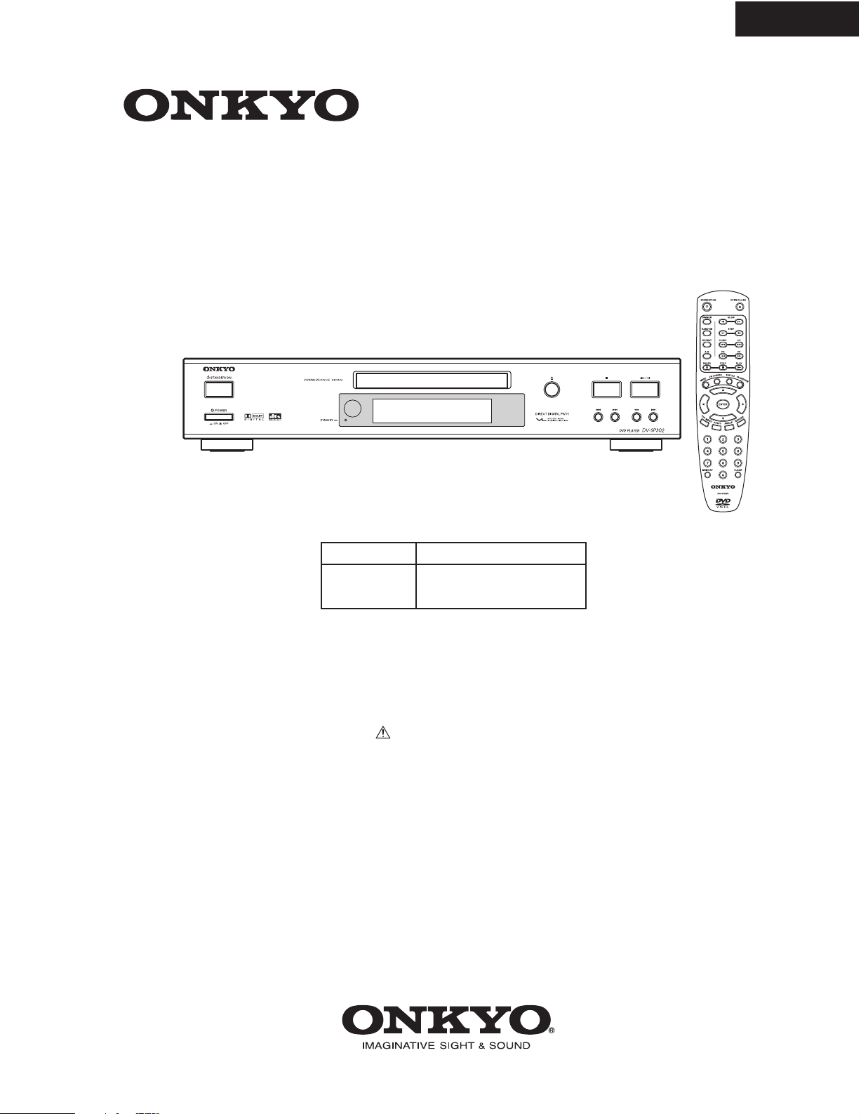
DVD PLAYER
MODEL DV-SP302
DV-SP302
Ref. No. 3814
092004
Black, Silver and Golden models
CDD
CUA, CUT,
120V AC, 60Hz
100-240V AC, 50/60Hz
CUK, CUR
SAFETY-RELATED COMPONENT
WARNING!!
THE MARK FOUND ON SOME COMPONENT
PARTS INDICATES THE CRITICAL FOR RISK OF
FIRE AND ELECTRIC SHOCK.
WHEN REPLACING, BE SURE TO USE PARTS OF
IDENTICAL DESIGNATION.
MAKE LEAKAGE-CURRENT OR RESISTANCE
MEASUREMENTS TO DETERMINE THAT EXPOSED
PARTS ARE ACCEPTABLY INSULATED FROM THE
SUPPLY CIRCUIT BEFORE RETURNING THE
APPLIANCE TO THE CUSTOMER.
RC-575DV
Page 2

SPECIFICATIONS
DVD Player
Power supply AC 120 V, 60 Hz (North America models)
AC 100-240 V, 50/60 Hz (Other models)
Power consumption 16 W
Weight 6.6 lbs, 3.0 kg
External dimensions (W x H x D) 17-1/8" x 3-3/16" x 11-1/8"
435 x 82 x 283 mm
Signal system PAL/NTSC
Frequency response Digital output 4 Hz to 22 kHz (48 kHz sampling)
DVD linear sound 4 Hz to 44 kHz (96 kHz sampling)
Signal-to-noise ratio (digital output) More than 90 dB
Audio dynamic range (digital output) More than 90 dB
Harmonic distortion (digital output) Less than 0.008%
Wow and flutter Below measurable level
DV-SP302
Outputs
Video output 1.0 V (p-p), 75 ohm negative sync., pin jack
S-video output (Y) 1.0 V (p-p), 75 ohm negative sync.,
(C) 0.286 V (p-p), 75 ohm Mini DIN 4-pin
PAL: (C) 0.300 V (p-p)
Component video output (Y) 1.0 V (p-p), 75 ohm negative sync.,
(PB)/(PR) 0.7 V (p-p), 75 ohm pin jack
Audio output Optical digital output -22.5 dBm, optical connector
Coaxial digital output 0.5 V (p-p), 75 ohm pin jack
Analog output 2.0 V (rms), 100 ohm pin jack (L, R)
Specifications and features are subject to change without notice.
Page 3
SERVICE PROCEDURE-1
SAFETY CHECK
(Only U.S.A. model)
After correcting the original service problem perform the
following safety check before releasing the set to the customer
Connect the insulating-resistance tester between the plug of
power supply cord and terminal GND on the back panel.
Specifications: More than 10M ohm at 500V
The lightning flash with arrowhead symbol, within an equilateral triangle, is
intended to alert the user to the presence of uninsulated "dangerous voltage"
within the product's enclosure that may be of sufficient magnitude to constitute
a risk of electric shock to persons.
The exclamation point within an equilateral triangle is intended to alert the user
to the presence of important operating and maintenance (servicing) instruction
in the literature accompanying the appliance.
LASER CAUTION
WARNING
RISK OF ELECTRIC SHOCK
DO NOT OPEN
AVI S
RISOUE DE CHOC ELECTRIQUE
NE PAS OUVRIR
DV-SP302
This unit contains a semiconductor laser system and is classified as a
CAUTION
VISIBLE AND INVISIVLE LASER RADIATION
WHEN OPEN DO NOT STARE INTO THE BEEM OR
VIEW DIRECTLY WITH OPTICAL INSTRUMENTS.
DO NOT PRESS ON THIS SURFACE
“CLASS 1 LASER PRODUCT”. So, to use this model properly, read
this Instruction Manual carefully. In case of any trouble, please contact
the store where you purchased the unit. To prevent being exposed to the
laser beam, do not try to open the enclosure.
CAUTION:
VISIBLE LASER RADIATION WHEN OPEN AND INTERLOCK
FAILED OR DEFEATED. DO NOT STARE INTO BEAM.
CAUTION:
THIS PRODUCT UTILIZES A LASER. USE OF CONTROLS OR
ADJUSTMENTS OR PERFORMANCE OF PROCEDURES OTHER
THAN THOSE SPECIFIED HEREIN MAY RESULT IN
HAZARDOUS RADIATION EXPOSURE.
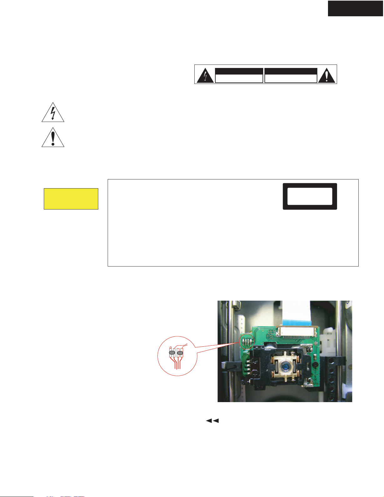
1.Remove the solder of Laser Diode shorting
1-1 Remove the bracket magnet.
1-2 Shorting the short land with solder.
1-3 Remove the FFC and other connectors.
The label on the right is
applied on the rear
panel except for USA
and Canadian models.
1. This unit is a CLASS 1 LASER PRODUCT and employs a laser
inside the cabinet.
2. To prevent the laser from being exposed, do not remove the
cover. Refer servicing to qualified personnel.
“CLASS 1 LASER
PRODUCT”
2. Factory setting (Initial setting)
2-1 Open the tray. Press 2 second the search button and
power key on remote controller (RC-575DV).
2-2 Displayed version of firmware on the FL tube.
2-3. At above condition, turn off the mechanical power switch.
Page 4
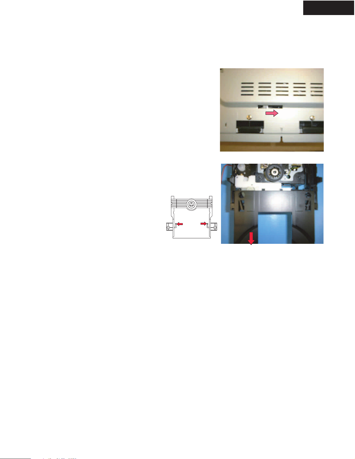
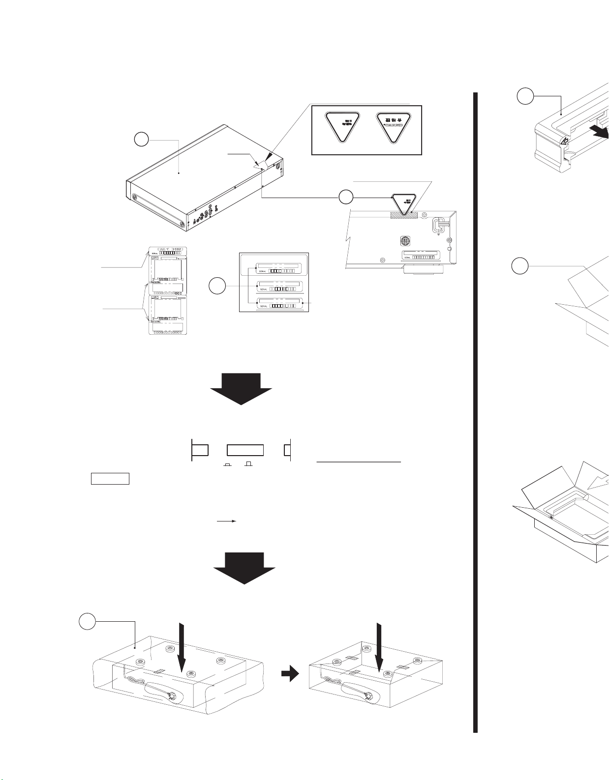
SERVICE PROCEDURE-2
Replace the DVD mechanism
1. Remove the top cover (six screws)
2. Remove two screws of both side of front panel.
3. Remove the bracket mecha. (two screws).
4. Shift the cam slider on bottom side. (See Fig-1)
5. Remove the tray.
6. Remove FFC, connector and one screw.
7. A tray is drawn out extending a nail. (See Fig-2)
DV-SP302
Bottom side
Fig-1
Tray
Page 5
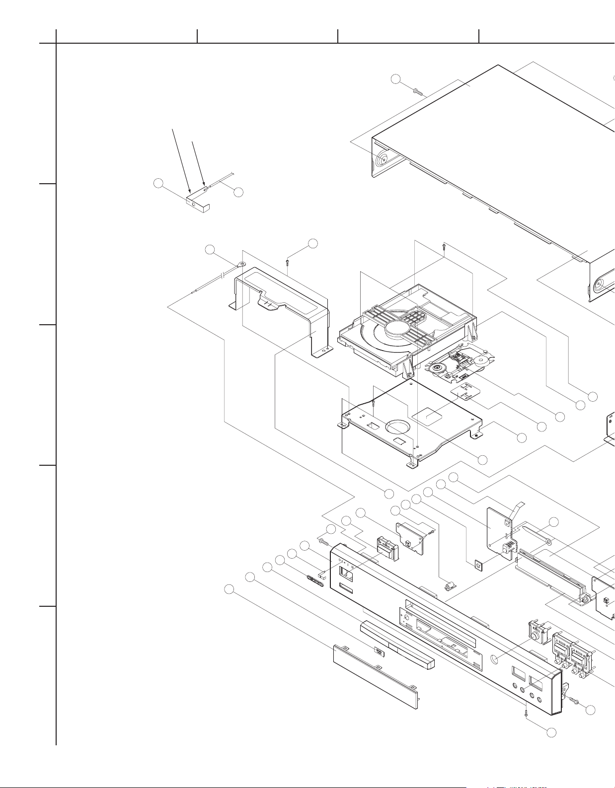
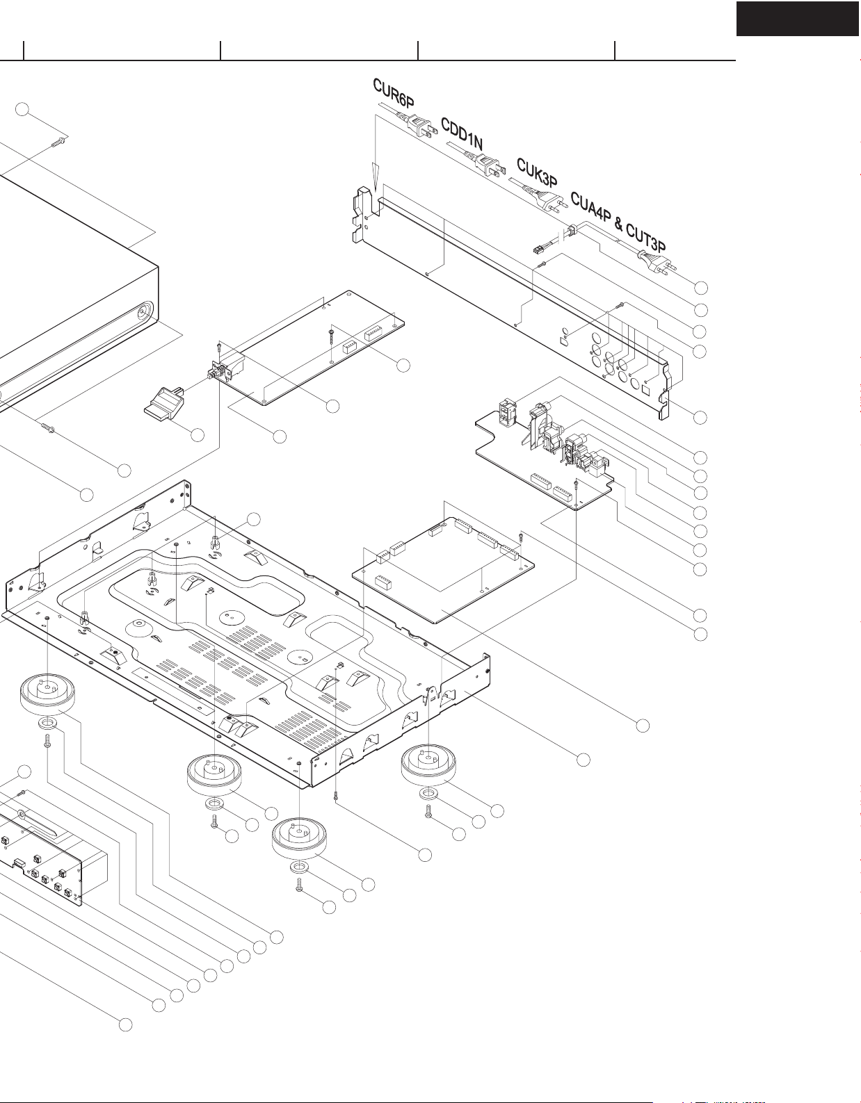
EXPLODED VIEW
A
1
2
3
4
5
BCDEFGH
S7
x2
S6
10
9
8
7
6
38
S6
5
4
S2
x 4
34
37
16
11
S2
x 2
4
1
4
2
3
S5
x 3
35
S2
x 2
39
1) Insert a plate in a panel front. Thereafter
2) Insert a wire in a hole of palte
and do soler.
39
38
40
S3
x 2
Page 6
DV-SP302
12
13
14
15
4
S5
x 11
S3
17
18
S3
17
18
S2
x 2
S3
17
18
19
20
21
S2
x 4
S2
22
23
24
25
26
27
28
S8
S4
x 11
30
29
S1
x 3
S2
x 2
31
36
x 3
32
S3
x 2
33
S3
18
17
40
S1 : 3 x 18 W/ Washer
S2 : 3 x 8 ZNY/ BH
S3 : 3 x 10 BK/ BH
or 3 x 8 Silver/ BH
S4 : 3 x 10 BK/ BH DOT
S5 : 2.6 x 8 ZNY/ PH
S6 : 3 x 8 BK/ FH
S7 : 3 x 10 BK/ BH
or 3 x 8 W/ Washer
S8 : 3 x 6 BK/ BH
S3
x 3
Page 7
DV-SP302
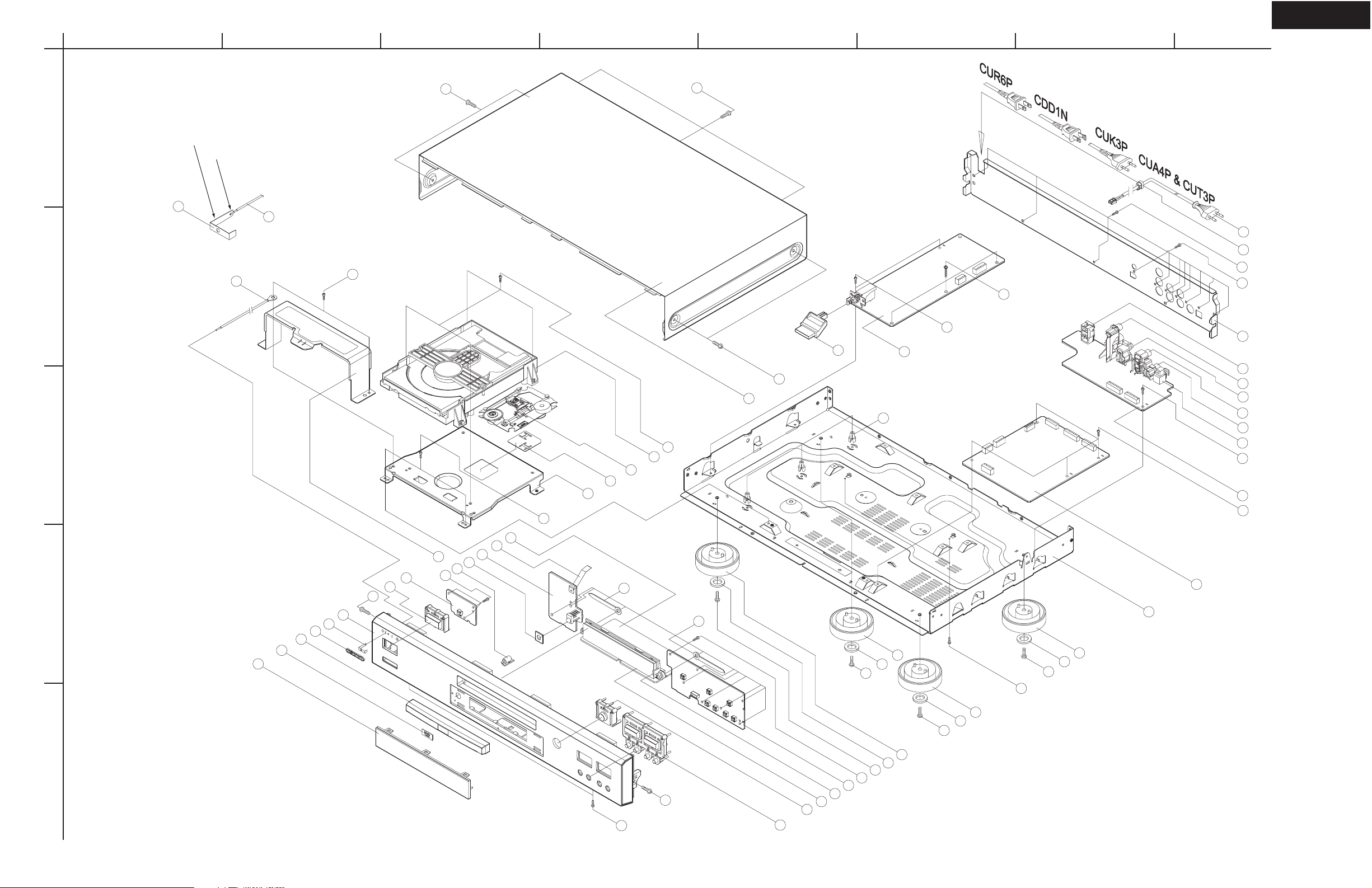
EXPLODED VIEW
A
1
2
3
4
5
BCDEFGH
S7
x2
S6
12
13
14
15
4
S5
x 11
S3
17
18
S3
17
18
S2
x 2
S3
17
18
19
20
21
S2
x 4
S2
22
23
24
10
9
8
7
6
38
S6
5
4
25
26
27
28
S8
S4
x 11
30
29
S1
x 3
S2
x 2
31
36
x 3
32
S3
x 2
33
S2
x 4
34
37
16
11
S2
x 2
4
1
4
2
3
S5
x 3
35
S2
x 2
39
1) Insert a plate in a panel front. Thereafter
2) Insert a wire in a hole of palte
and do soler.
39
38
S3
18
17
40
40
S1 : 3 x 18 W/ Washer
S2 : 3 x 8 ZNY/ BH
S3 : 3 x 10 BK/ BH
or 3 x 8 Silver/ BH
S4 : 3 x 10 BK/ BH DOT
S5 : 2.6 x 8 ZNY/ PH
S6 : 3 x 8 BK/ FH
S7 : 3 x 10 BK/ BH
or 3 x 8 W/ Washer
S8 : 3 x 6 BK/ BH
S3
x 3
S3
x 2
Page 8
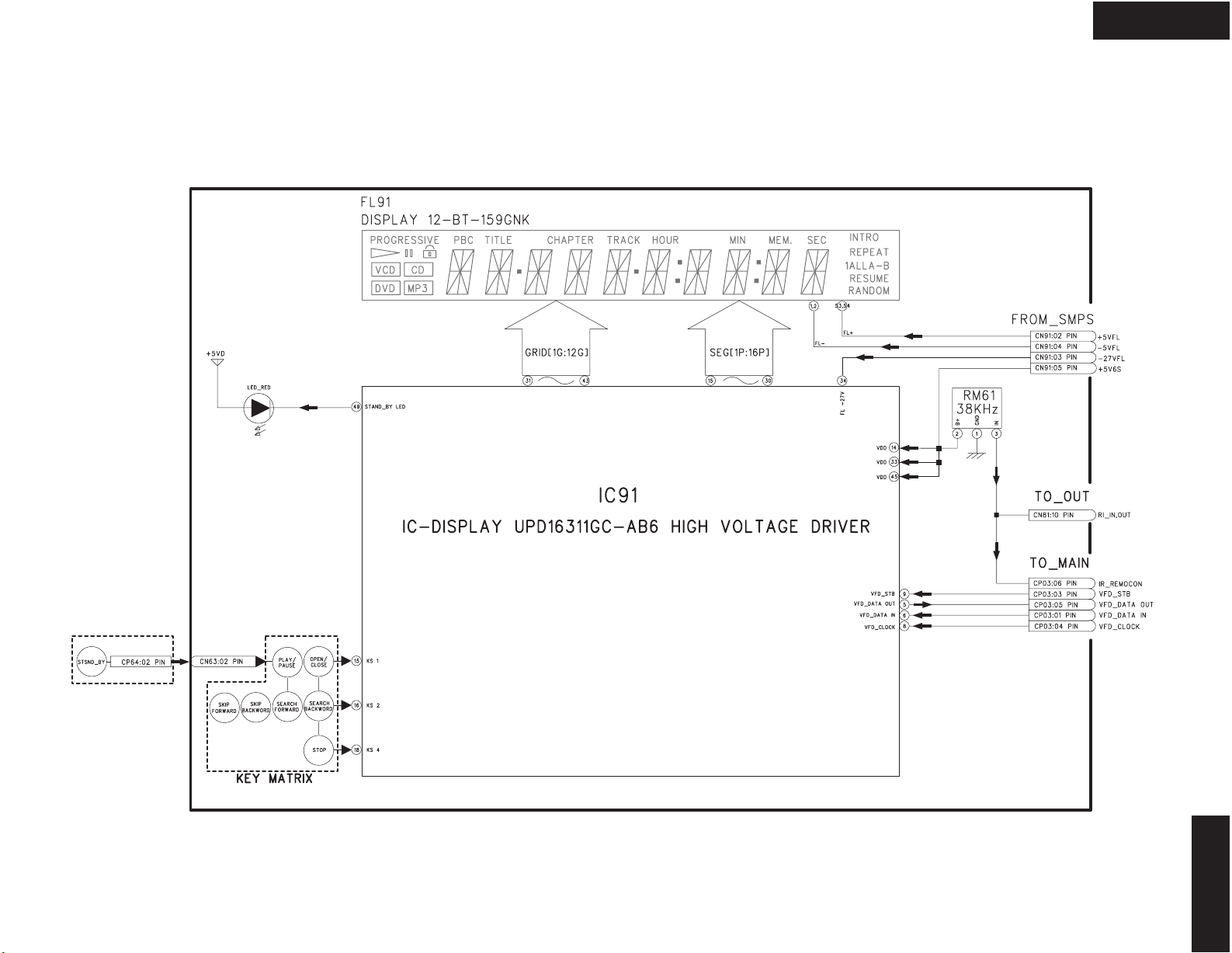
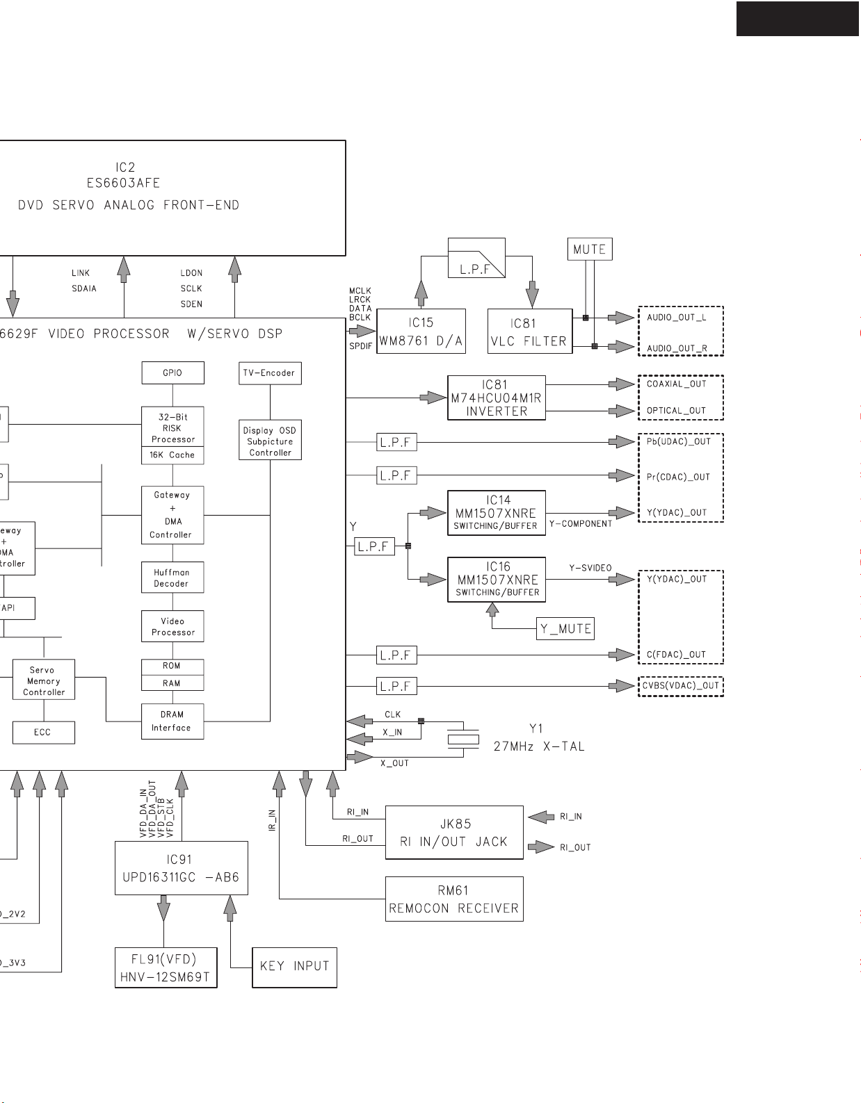
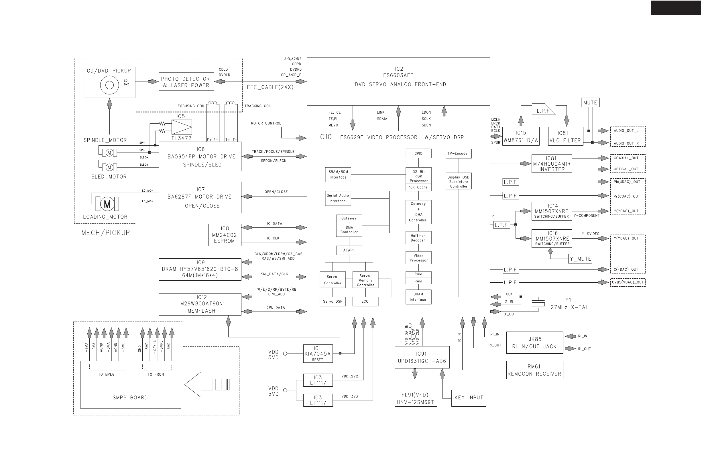
BLOCK DIAGRAM
FRONT DISPLAY SECTION
DV-SP302
DV-SP302
Page 9
BLOCK DIAGRAM
OVERALL
Page 10
DV-SP302
Page 11
DV-SP302
BLOCK DIAGRAM
OVERALL
Page 12
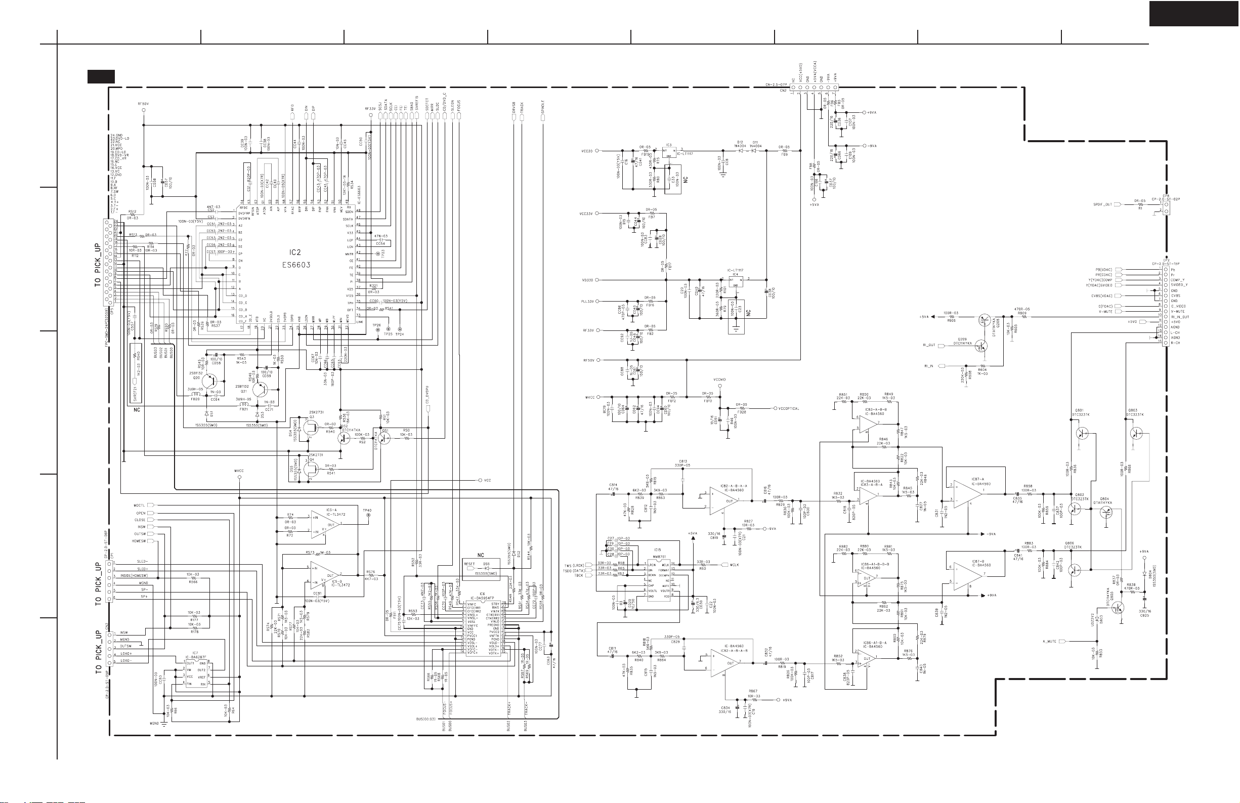
SCHEMATIC DIAGRAM
U20 : DVD MAIN CIRCUIT BOARD-2/2
A
1
2
3
4
5
BCDEFGH
Page 13
DV-SP302
From Power supply unit
To Output board
Page 14
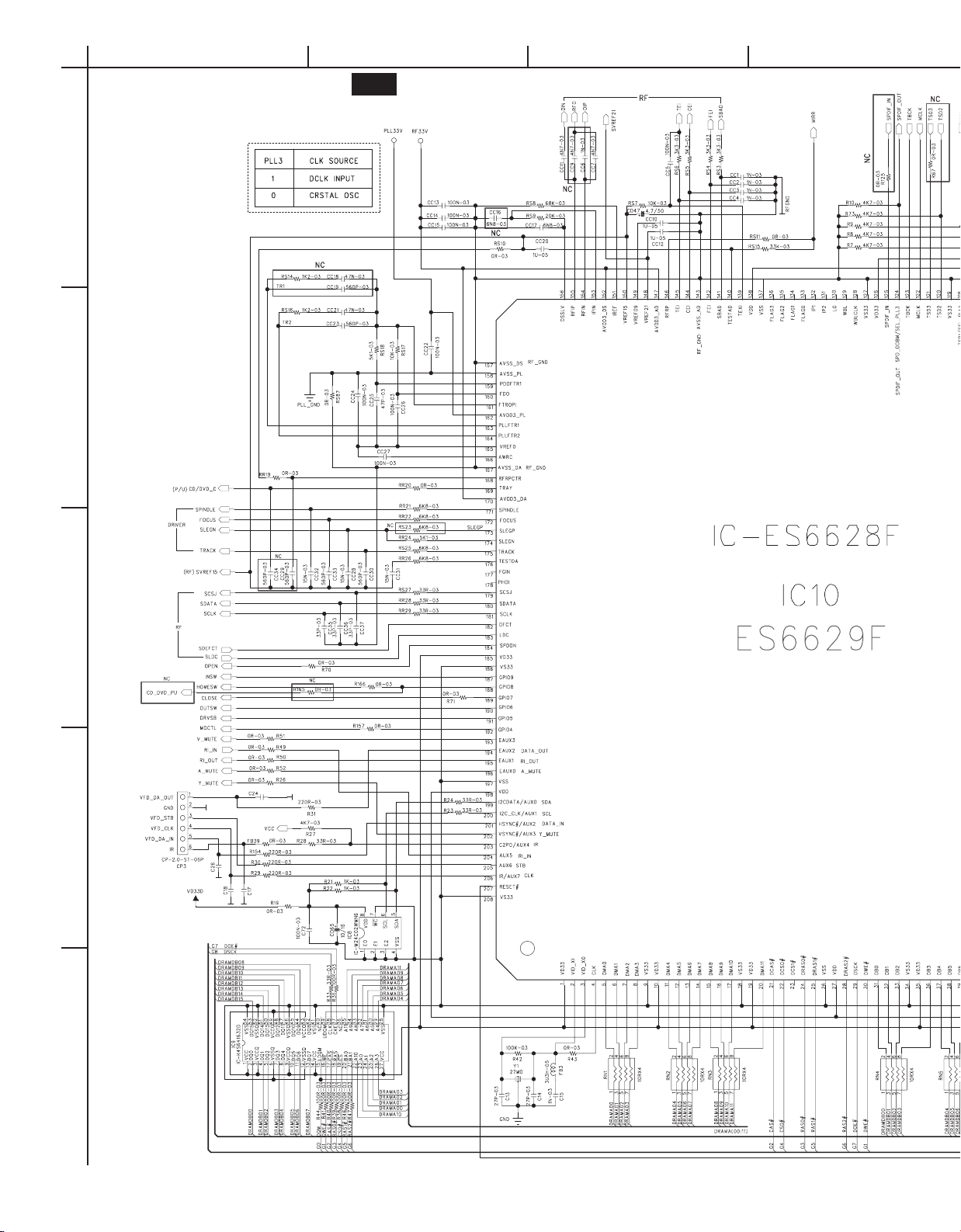
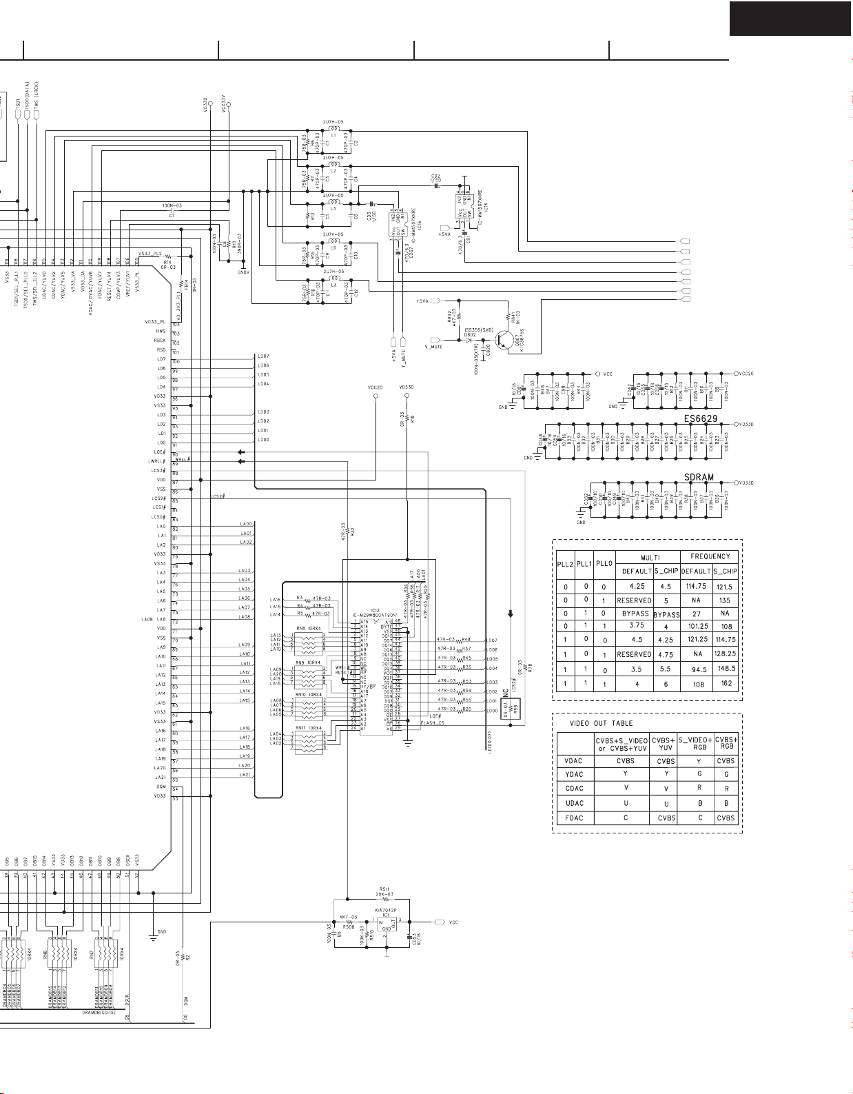
SCHEMATIC DIAGRAM
U20 : DVD MAIN CIRCUIT PC BOARD-2/2
A
1
2
3
4
5
BCDEFGH
From Front board
Page 15
DV-SP302
150R-03
150P-03
150P+
150R-03
Y
PB (UDAC)
PR (CDAC)
Y (YDAC) COMP.
Y (YDAC) SVIDEO
CVBS (VDAC)
C (FDAC)
V-MUTE
Pb
PR
CV
C
Page 16
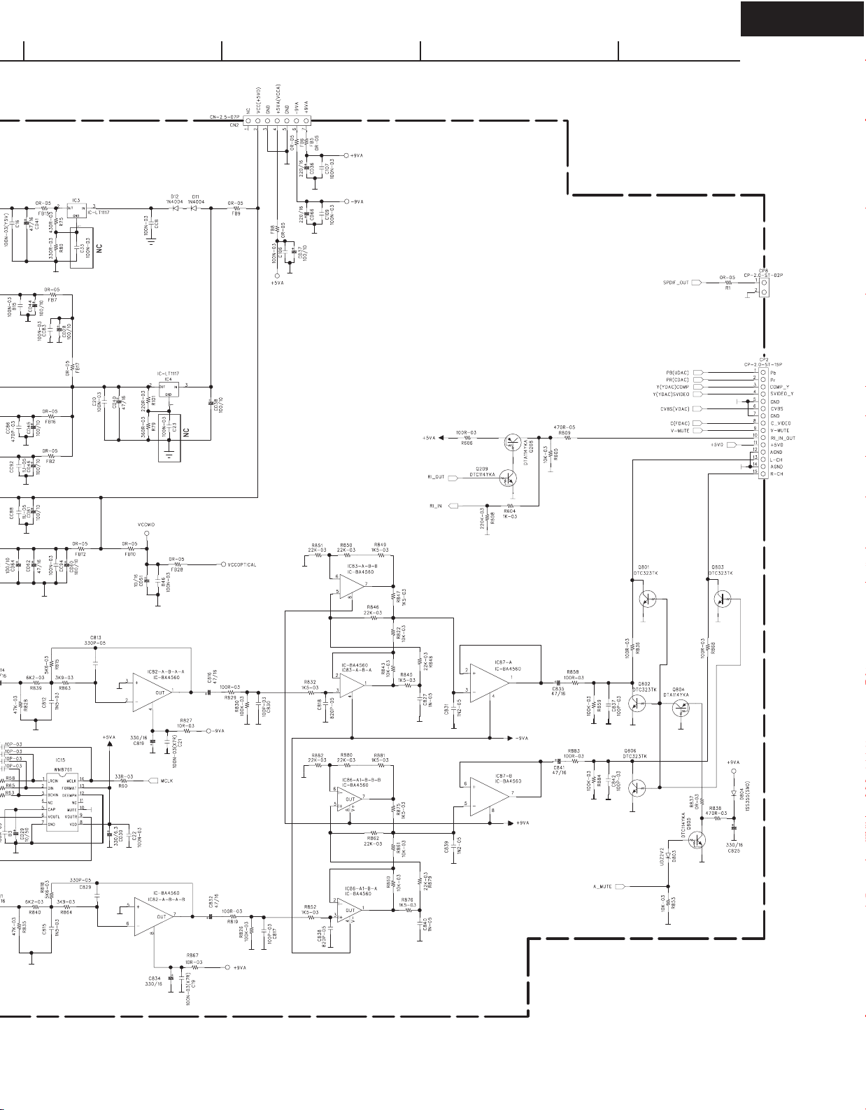
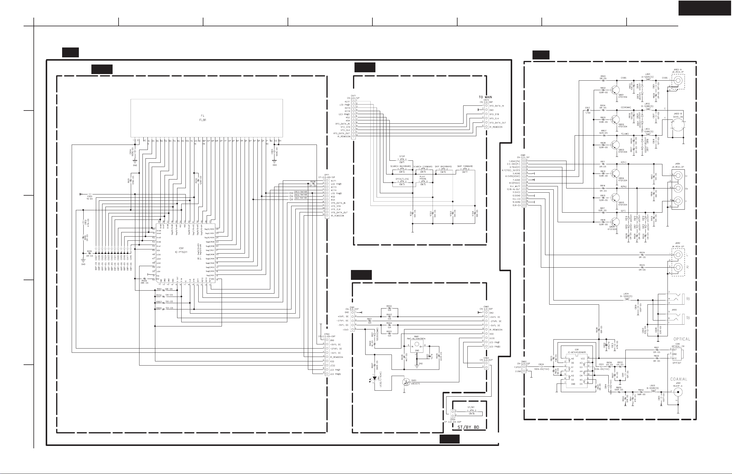
SCHEMATIC DIAGRAM
A
1
2
3
4
5
BCDEFGH
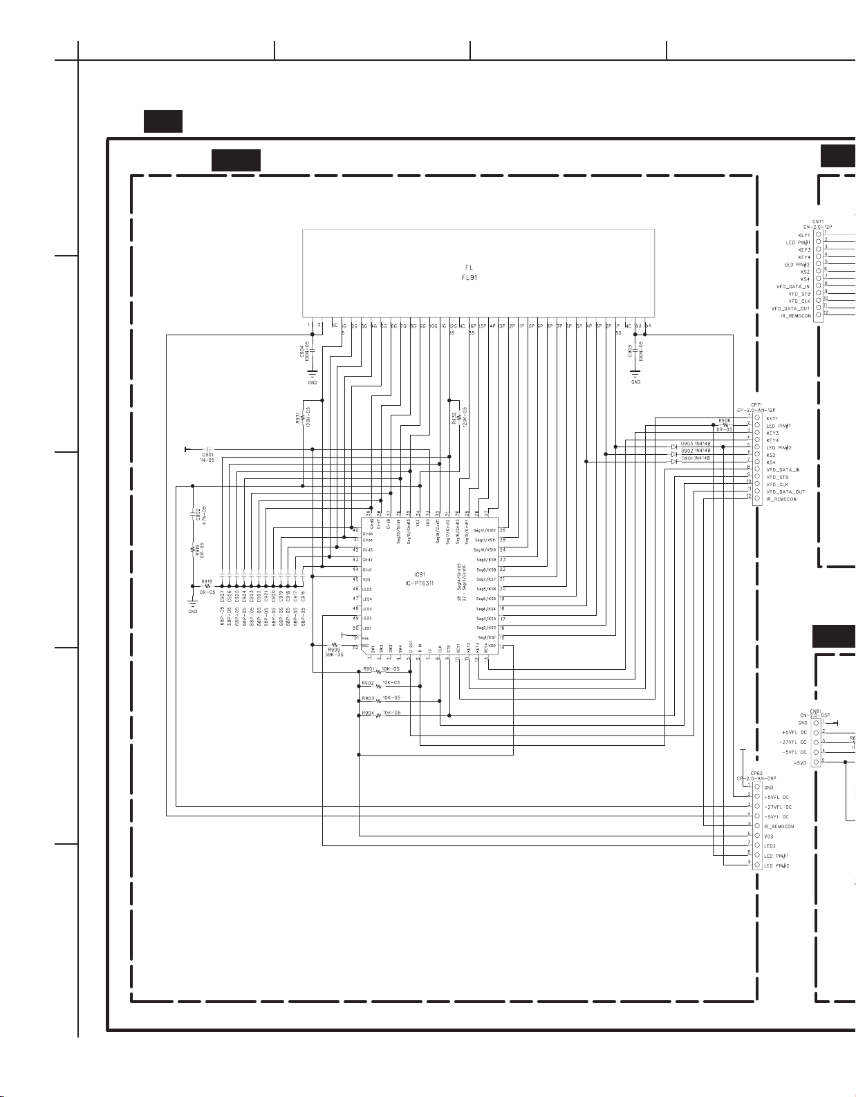
U4 : FRONT DISPLAY PC BOARD
U4-1 : FL TUBE PC BOARD
U4-2 : KEY SWITCH PC BOARD
U4-4 : REMOTE SENSOR PC BOARD
To Power supply unit
From Remote
sensor board
From Key
switch board
From FL tube board
Page 17
DV-SP302
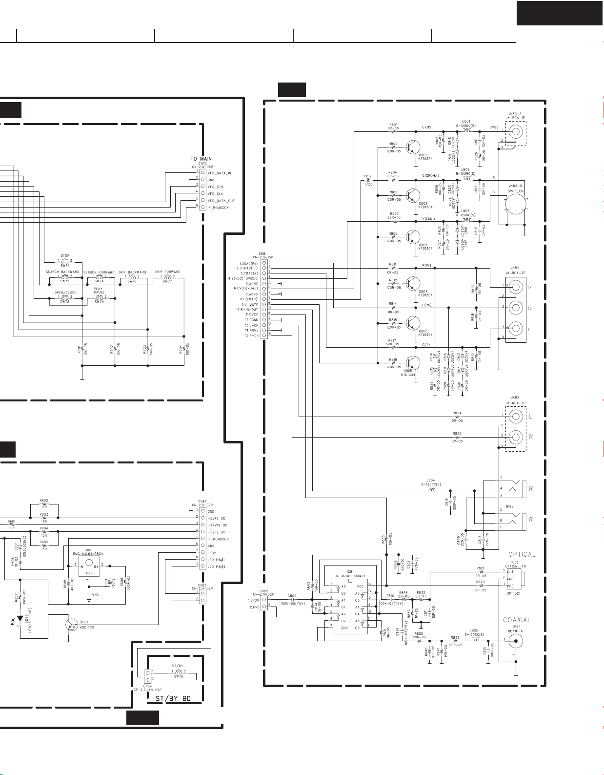
U21 : OUTPUT TERMINAL PC BOARD
U4-3 : STANDBY SWITCH PC BOARD
To FL display board
To DVD main board
To D VD
main board
Optical
Coaxial
Page 18
DV-SP302
SCHEMATIC DIAGRAM
A
1
2
3
4
5
BCDEFGH
U4 : FRONT DISPLAY PC BOARD
U4-1 : FL TUBE PC BOARD
U4-2 : KEY SWITCH PC BOARD
U4-4 : REMOTE SENSOR PC BOARD
U21 : OUTPUT TERMINAL PC BOARD
U4-3 : STANDBY SWITCH PC BOARD
To Power supply unit
From Remote
sensor board
To FL display board
From Key
switch board
From FL tube board
To DVD main board
To D VD
main board
Optical
Coaxial
Page 19
DV-SP302
SCHEMATIC DIAGRAM
U20 : DVD MAIN CIRCUIT BOARD-2/2
A
1
2
3
4
5
BCDEFGH
From Power supply unit
To Output board
Page 20
DV-SP302
SCHEMATIC DIAGRAM
U20 : DVD MAIN CIRCUIT PC BOARD-2/2
A
1
2
3
4
5
BCDEFGH
From Front board
150R-03
150P-03
150P+
150R-03
Y
PB (UDAC)
PR (CDAC)
Y (YDAC) COMP.
Y (YDAC) SVIDEO
CVBS (VDAC)
C (FDAC)
V-MUTE
Pb
PR
CV
C
Page 21
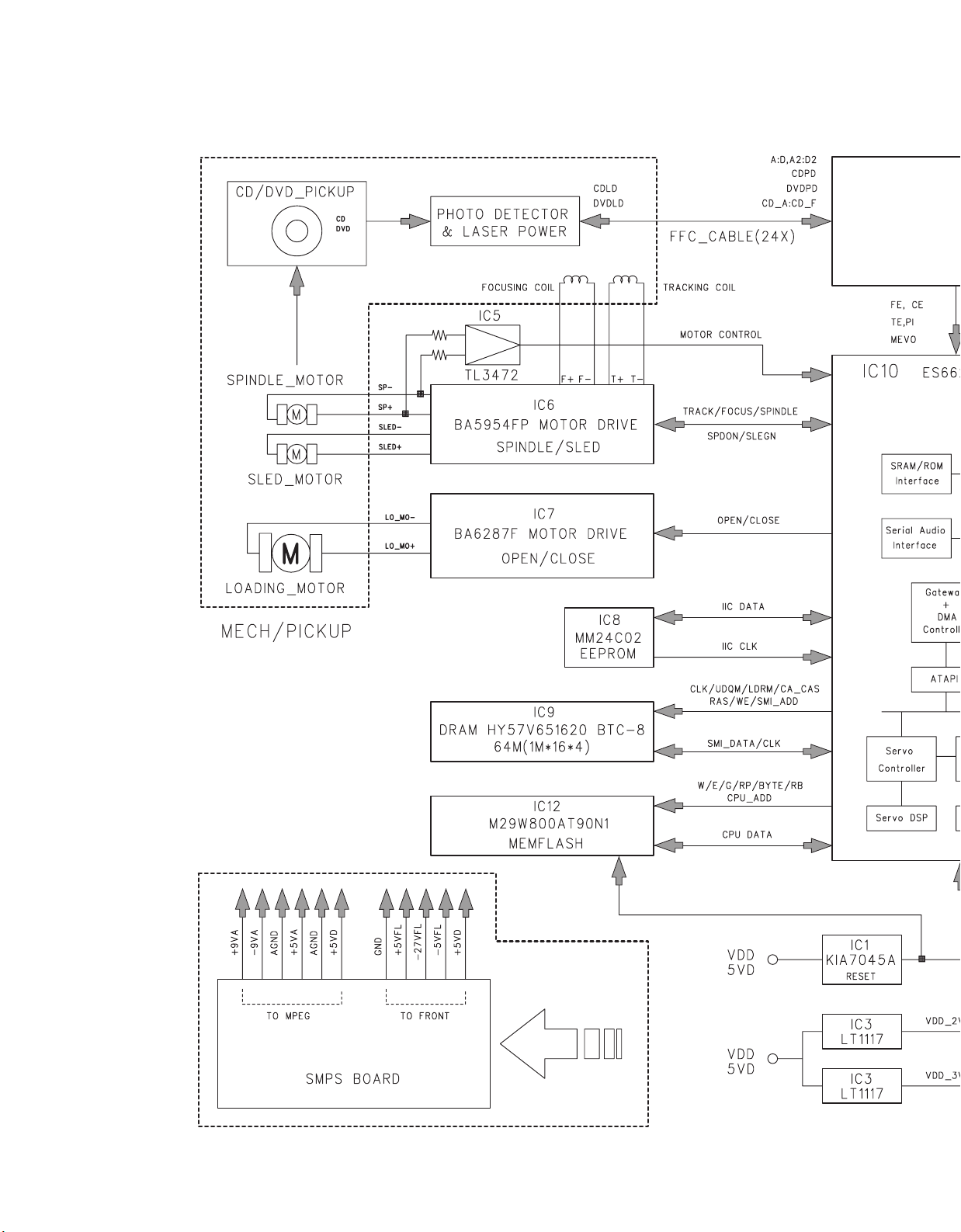
PCBOARD CONNECTION DIAGRAM
31
POWER SUPPLY UNIT
MECHA.
PICK-UP
CMS-S71SG6C
DV-SP302
U21
OUTPUT TERMINAL BOARD
U20
DVD MAIN BOARD
U4-3
STANDBY
SWITCH BOARD
U4-1
From power
supply board
U4-4
REMOTE
SENSOR BOARD
U4 FRONT DISPLAY BOARD: (U4-1) + (U4-2) + (U4-3) + (U4-4)
FL TUBE
BOARD
U4-2
KEY
SWITCH BOARD
DV-SP302
Page 22
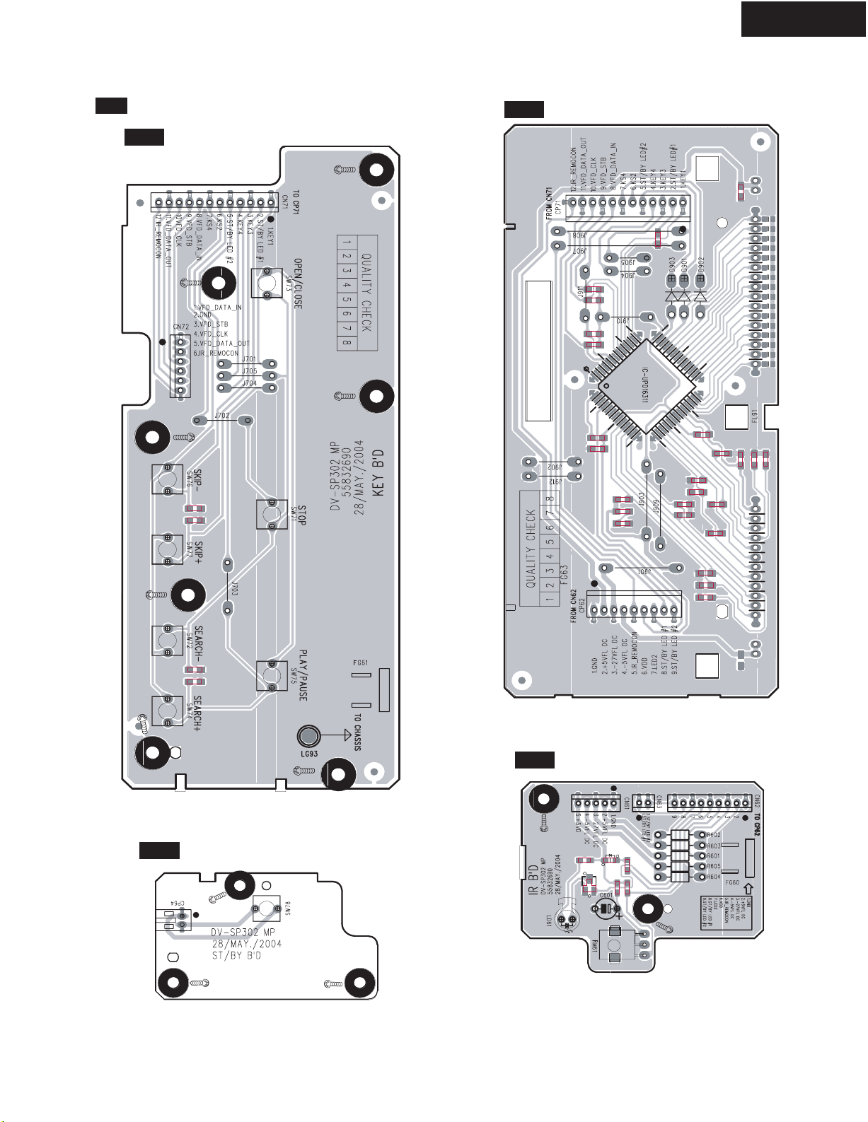
PRINTED CIRCUIT BOARD VIEW FROM COMPONENT SIDE-3
DV-SP302
U4 : FRONT DISPLAY BOARD
U4-2 : KEY SWITCH BOARD
R703
R704
U4-1 : FL TUBE BOARD
R906
R904
R903
5
50
R931
C902
R919
13
10
45
39
40
C922
C921
C920
C919
R902
R901
R909
C901
1
C905
C943
C942
C941
C940
C939
C938
C937
C936
C935
C934
35
R910
20
R932
C933
C932
C931
C930
C929
C928
P16 P15 P14 P13 P12 P11 P10 P9 P8 P7 P6 P5 P4 P3 P2 P1
IC91
30
C927
C925
C924
C926
C923
14
R701
R702
U4-3 : STANDBY SWITCH BOARD
C917
C916
C918
C904
U4-4 : REMOTE SENSOR BOARD
D601
R607
R606
R609
Q601
R608
1G 2G 3G 4G 5G 6G 7G 8G 9G 10G 11G 12G
Page 23

PRINTED CIRCUIT BOARD VIEW-1
U20 DVD MAIN BOARD-1
DV-SP302
Top view
Page 24

PRINTED CIRCUIT BOARD VIEW-2
U20 DVD MAIN BOARD-2
DV-SP302
Bottom view
Page 25

PRINTED CIRCUIT BOARD VIEW FROM SOLDERING SIDE-4
U21 OUTPUT TERMINAL PC BOARD
5
1
4
JK85
2
3
6
Component side view
DV-SP302
JK82
JK81
JK84
CN81
JK83
C812
IC86
CN83
C802
Page 26
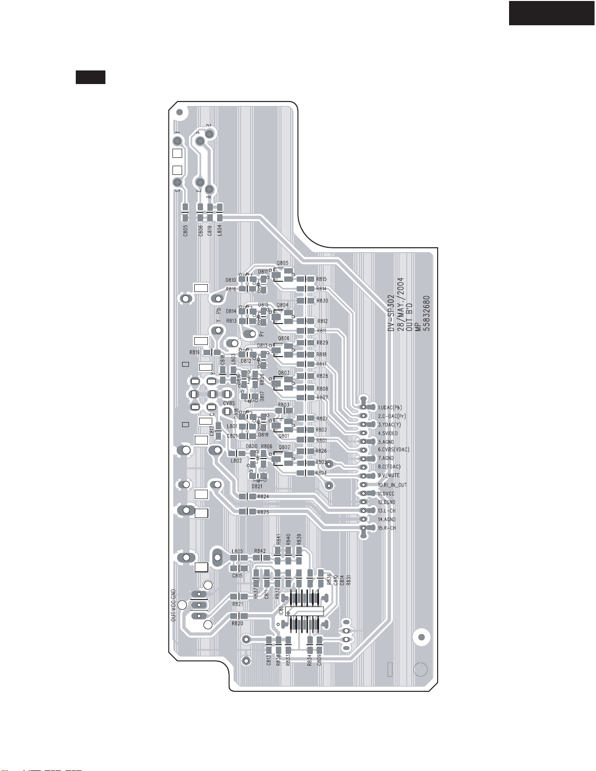
PRINTED CIRCUIT BOARD VIEW FROM SOLDERING SIDE-5
U21 OUTPUT TERMINAL PC BOARD
Soldering side view
DV-SP302
Page 27
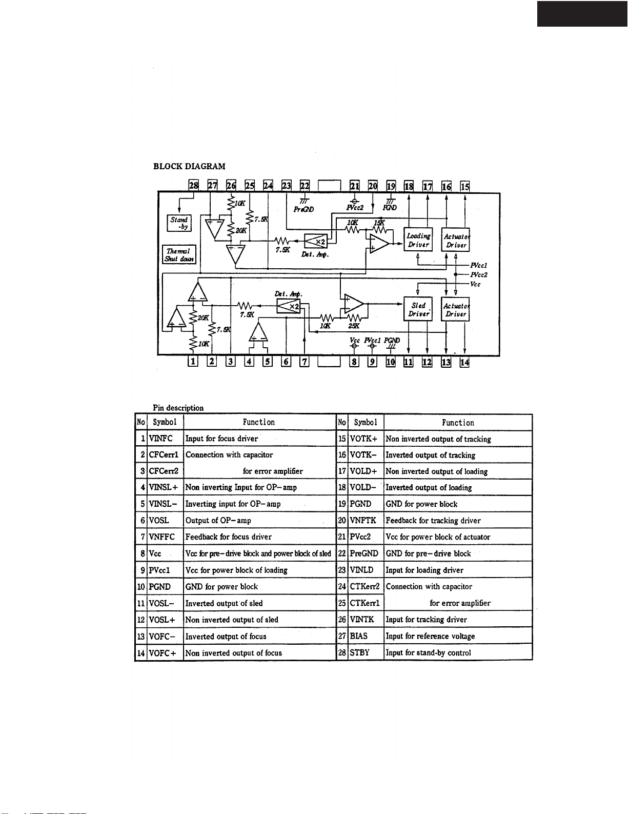
IC BLOCK DIAGRAM/ TERMINAL DESCRIPTION
IC6 : BA5954 MOTOR DROVER
DV-SP302
Page 28

IC BLOCK DIAGRAM/ TERMINAL DESCRIPTION
1 3
2 6
12
25
24
23
22
21
20
19
18
17
1 6
2 9
3 1
3 2
2 8
2 7
3 0
5 5
56
57
58
59
60
61
62
63
64
5 2
5 0
4 9
5 3
5 4
5 1
3 6
37
3 3
RX
EV
NA
NN
NP
IP
IN
YP
AC
PA
IP
IN
ON
OP
IN
DC
VO
IN
PF
MB
MP
RR
ON
NB
PD
PD
LD
LD
VC
PB
_E
_F
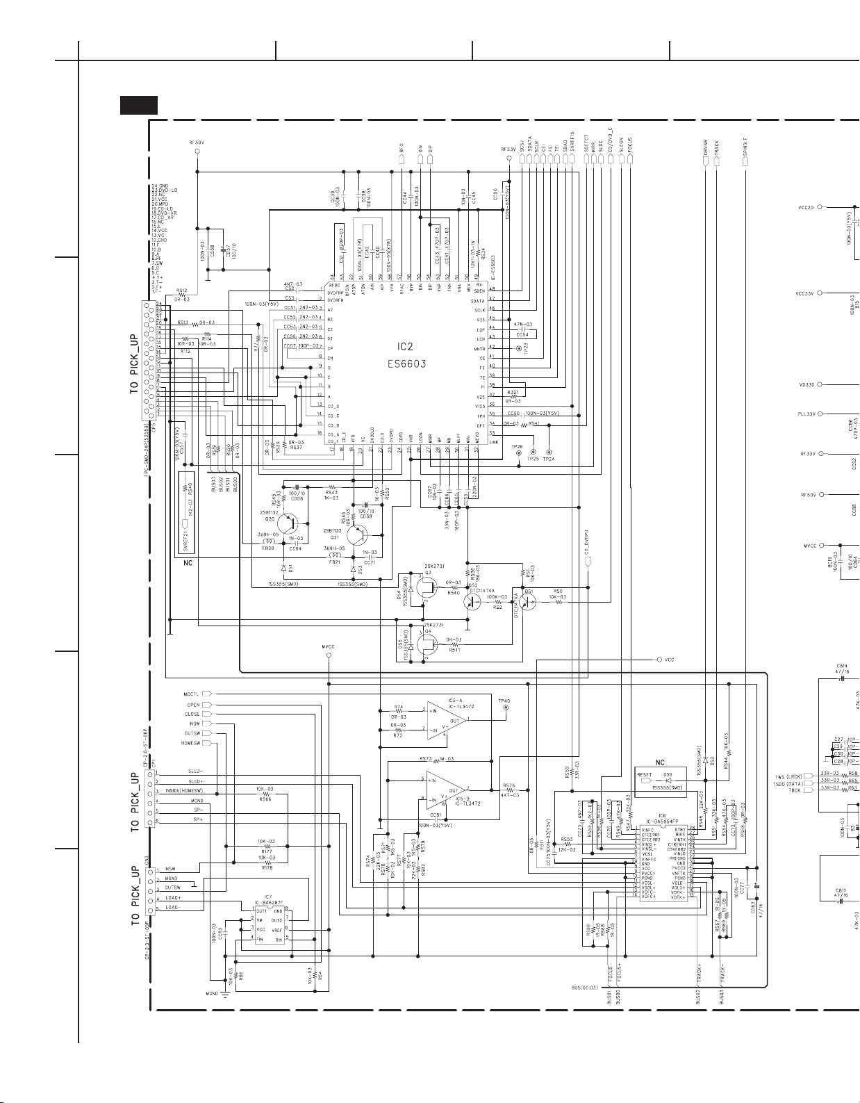
IC2 : ES6603 DVD SERVO F/E-(1)
DV-SP302
RX
MEV
V NA
F NN
F NP
DIP
DIN
B YP
R FAC
V PA
AIP
AIN
AT ON
A T OP
4 8 36
47 46 45 44 43 42 41 40 39 38 37
49
50
51
52
53
54
55
56
57
58
59
60
61
62
ES6603S
3 5 34 33
32
31
30
29
28
27
26
25
24
23
22
21
20
19
ME VO
MIN
MLMLPF
MB
MP
MIRR
LDON
V NB
C D PD
DV DPD
C D LD
DV DLD
VC
V PB
R F S IN
R FDC
63
64
1 13
2 3 4 5 6 7 8 9 10 11 12
1 4 15 16
18
17
C D _E
C D _F
Page 29

IC BLOCK DIAGRAM/ TERMINAL DESCRIPTION
IC2 : ES6603 DVD SERVO F/E-(2)
Name Pin Numbers I/O Definition
DVDRFP,
DVDRFN
A2, B2, C2, D2 3:6 I
CP, CN 7, 8 — Differential phase tracking low-pass filter pins. Connect CP to CN via capacitors.
D, C, B, A 9:12 I Photo detector interface inputs from the main beam photo matrix.
CD_D, CD_C,
CD_B, CD_A
CD_F, CD_E
VPB 19 P Servo block power supply.
VC 20 O Reference voltage out (VPB/2). Output impedance is less than 50
DVDLD 21 O DVD APC output; controls laser power for DVD.
CDLD 22 O CD APC output; controls laser power for CD.
DVDPD 23 I DVD APC input.
CDPD 24 I CD APC input.
VNB 25 G Servo block ground.
LDON 26 I APC On/Off control. A high level activates LD output. (open is low)
MIRR 27 O Mirror detect output.
MP, MB 28, 29 I Mirror top and bott
MLPF 30 I Mirror low-pass filter pins. Connected to VPB pin 19 via a capacitor.
MIN
MEVO 32 O
LINK 33 I,O
DFT 34 O
TPH 35 I Pull-In top hold. Connected to VPB pin 19 via a capacitor.
V125 36 O 1.25V servo block reference voltage output.
V25 37 P 2.5V servo output reference power supply.
PI 38 O
TE 39 O Tracking error output reference to V125 pin 36.
FE 40 O Focusing error output reference to V125 pin 36.
1, 2 I Differential RF signal attenuator inputs.
AC coupled photo detector interface inputs for the differential phase detector (DPD)
from the main beam photo matrix.
13:16 I CD photo detector i
17, 18 I CD photo detector interface inputs from the CD side beam photo detector; used for
CD tracking detection.
31 I RF input signal for mirror. AC coupled inputs for the mirror detection circuit from
MEVO pin 32.
RFDC bottom envelope out. Pull-In or bottom clamped RF envelope signal output
for mirror detection.
Linking Signal In/Mirror Monitor Out. In the linking area, the mirror and tracking
error outputs are disabled when this pin goes high. When the monitor output signal
is selected by the Control H register, mirror-related signals can be observed.
Defect output. When the Pull-In signal level is below the detection level, or when
the RF signal level is below the detection level, the DFT output goes high. The
defect output is selected by the serial port.
Pull-In signal out. The summing signal output of A, B, C, D, or CD_A, CD_B, CD_C,
or CD_D. Reference to V25/3.
terface inputs from the main beam photo matrix.
n
om
hold pins.Connected to VPB pin 19 via capacitors.
DV-SP302
Page 30

IC BLOCK DIAGRAM/ TERMINAL DESCRIPTION
6.
s.
CP
ft
lla
nect t
c-
r.
po
y.
fromom E E
8.
da
I/O.O.
. E
by
an
ac
l.
sis
nec
12
sis
..
botttt
ope. .
r.
po
d.
, F
ou
r.
npu
r.
r.
t.
po
y.
s.
s.
gna
t.
ded R R
ou
t.
on
IC2 : ES6603 DVD SERVO F/E-(3)
DV-SP302
Name Pin n Numbers I/I/O Definition
CE 41 O Cenenter r error r ououtput t referenence t to V V125 p pinin 3 36.
MNTR 42 O Mononitor r ouout t sigignalal. . Outpuput t is s selelectablele b by r regegister s settttingngs.
LCN, , LCP
V33 45 P 3.3V V ououtpuput t bubuffers po
SCLK 46 I Serialal c clockck fr
SDATATA 47 I/I/O Serialal da
SDEN 48 I Serialal d data e enabablele. E
RX 49 I Referencece r resis
MEV 50 I RFDC bo
VNA 51 G RF b blolockck a andnd seserialal po
FNN, F
NP 52, 5 53 O Differentialal ou
DIP, D DIN 5454, , 55 I Differenentialal a analogog inpu
BYP 56 I AGC a amplilifieier r gainin b bypass. T Tieded t to V VPA A viaia a a capacacitor.
RFAC 57 O Singnglele-endeded R RF F ououtpuput.
VPA 58 P RF b blolockck a andnd seserialal po
AIAIP, A AIN 5959, , 60 I Differentialal A AGC a ampmplifieier r inpnputs.
ATON, , ATOP 6161, , 62 O Differentialal a attttenuator o outpuputs.
RFSISIN 63 I Sininglele-endeded R RF F signa
RFDC 64 O Singnglele-ended
4343, , 44 I Lensns s shihift
itor.
offseset t cancella
ta I/
om e envevelope
tputs o of f equaualizezer/f/fililter.
tionon lolow-pasass f fililter r pinins. C Connec
wer r supppply.
S66x8.
nableded by
tor. . Connec
rt t ground.
ts t to t thehe R RF s singnglele-endnd ououtput t bubuffer andnd f fullll w waveve r recectifier.
rt t popower s supplply.
l a attenuauator r inpnput.
F summmmingng ou
an
ac
tiveve-highgh s signgnal.
teded t to g grounund v viaia a a 12
Connececteded t to V VPA p pinin 5858 v viaia a a c capacicitor.
tput.
.0k0k, , 1%1% r resis
LCN t to L LCP v viaia a a capapac-
tor..
Page 31
AIN
IC BLOCK DIAGRAM/ TERMINAL DESCRIPTION
IC2 : ES6603 DVD SERVO F/E-(4)
Block diagram
DV-SP302
DVDRFP
DVDRFN
DVDPD
OUTPUT INHIBIT
CCR b4-0
FE offset
CBR b3-2
Buff
CTCR b3-0
GCA
0-+8dB,4bit
LPF
ATT
Pol.sel
Buf(-12dB)
GCA
CGR b5-4
Gain
CGR b1
5
Offset
cansel
TOPHLD
CGR b0
OUTPUT INHIBIT
CO gain
4
SUB
CFR b4
CEFDB
CDR b7
LINKEN
RFA C
PII
SEL
CBR b1-0
SEL
CBR b5-4
TE MASK sel
MON
SEL
3
TE
RST
for TE,FE & CE output ref.
CDR b2
CDR b3
CCR b7
DISK DET
VP B
VN A
CDR b6
HLDEN
BYP
RX
FE
PI
TPH
DFT
2
RFDC
2
CE
MNTR
LCP
LCN
CP
CN
TE
V125
V25
VC
SDEN
SDATA
SCLK
V33
VNB
RFCR b3
AGC HOLD
AGC
CHARGE
PUMP
+/- 6dB 4bit
GCA
4
FOCR b3-0
FO Gain
COMP
2
DAC
PI
FE
TE
CE
V25
V125
V25/3
PIOR b7-5
Offset
GCA
cancel
3
6
CFR b7-5
TRCR b5-0
TR Gain
TR offset
for PI output ref.
LINK
V25/3
SERIAL PORT
REGISTER
VCI for servo input
MUX
MIRR
V25/2
VC
V33 for Output buff
VP A
ATOP
ATON
AIN
AIP
FCCR b6-0
FBCR b6-0
SIGR b2-0
12dB is added
@high gain mode
(CDR b5=1)
(CDR b5=1) @high gain mode
VC
IMPUT
BIAS
INPUT IMP SEL
+/- 4dB
GCA
4
TRCR2 b3-0
3B
Comp.
TRCR b6
DPD COMP HYS ON
DV D LD
2
RFCR b5-4
B + D
SUM
A + C
A + D
B + C
AG C O
Btm Env
ME V
AGC
SSOUT
Clamp
& Env
2
CAR b1-0
Env/Clamp
Tenvb
Amp.
RESUM
PHASE
DETECTOR
PHASE
DETECTOR
AGC BT M EN V
Tenv b
PII
MUX
ME V O
MIN
+-3dB
CDR b5
High gain
CTCR b5-4
MEVO SEL
TOPHLD
TOPHLD
MUX
Btm clamp
2
CAR b3-2
SIGDET
GCA
2
& clip
2
RFCR b7-6
INPUT IMP SEL
A
B
C
D
12dB is added
@high gain mode
6dB is added
@high gain mode
(CDR b5=1)
GCA
GCA
3
RFCR b2-0
(CDR b5=1)
GCA
GCA
GCA
GCA
3
RFCR b2-0
GCA
ATT
GCA
GCA
GCA
GCA
GCA
GCA
GCA
CCR b5
SIGR b7-4
SUM
APC SEL
DVD/CD
ATT
4D
LDON
4
w/LPF
w/LPF
w/LPF
w/LPF
3
SIGR b2-0
EQ
EQ
EQ
EQ
TRCR2 b6-4
DPD EQ
12dB is ad ded
3
Dual APC
CD L D
MUX
RFSIN
SIGR b3
INPUT S EL
A
MUX
CD_A
B
CD_B
C
CD_C
D
CD_D
PDCR b3
CD/DVD
CD_E
CD_F
A2
B2
C2
D2
CDR b4
LD H/L
CDPD
14
PROGRAMMABLE
EQUALIZER
FILTER
DIFFERENTI
Level
DAC
+/- 4dB
4
70kHz
LPF
MRCR2 b7 -0
droop rate
control
TOP HLD
TOP ENV
BTM HLD
BTM ENV
FNP
ATOR
FOCR b7-4
FS gain
FNN
AGCO
MUX
PDCR b3
CD/DVD
DIP
DIN
FULL WAVE
RECTIFIER
70kHz
LPF
5
PIOR b4-0
PI offset
Offset
cancel
CTCR b7
BCA DET
Offset
cancel
4
CER b4-0
CE offset
3
CFR b2-0
CE-ATT
CFR b3
CEPOL
LPF
TRCR2 b7
CP/CN
Low Imp
CHR b7-6
Mirr Defect
Comp ATT
MRCR b6-4
Mirr Comp
ATT Level
MUX
MB
MP
CONTROL
Signals
To each block
2
3
ATT
MUX
ATT
offset
Vref
MUX
ML PF
Page 32

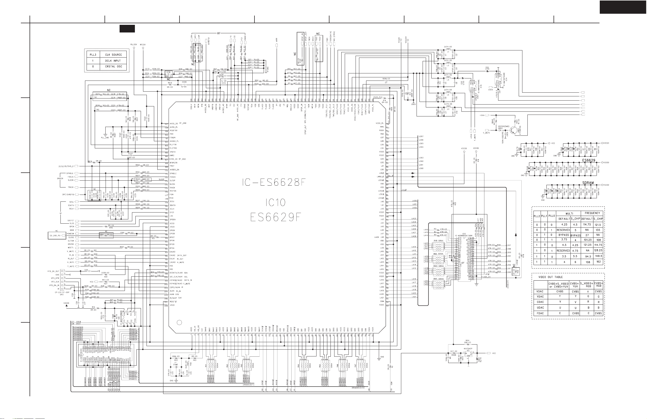
IC BLOCK DIAGRAM/ TERMINAL DESCRIPTION
IC10 : ES6629 VIDEO PROCESSOR-(1)
PINOUT DIAGRAM
IREF
RFIP
DSSLV
AVSS_DS
AVS S_ PL
PDOFTR1
FDO
FTROPI
AVDD3_PL
PLLFTR1
PLLFTR2
VREF0
AWRC
AVSS_DA
RFRPCTR
TRAY
AVDD3_DA
SPINDLE
FOCUS
SLEGP
SLEGN
TRACK
TESTDA
FGIN
PHOI
SCSJ
SDATA
SCLK
DFCT
LDC
SPDON
VD33
VS33
GPIO9
GPIO8
GPIO7
GPIO6
GPIO5
GPIO4
EAUX3
EAUX2
EAUX1
EAUX0
VSS
2
I
2
I
IOW#/HSYNC#/AUX2
IOR#/VSYNC#/AUX3
VDD
CDATA/AUX0
C_CLK/AUX1
C2PO/AUX4
AUX5
AUX6
IR/AUX7
RESET#
VS33
RFIN
154
155
156
157
158
159
160
161
162
163
164
165
166
167
168
169
170
171
172
173
174
175
176
177
178
179
180
181
182
183
184
185
186
187
188
189
190
191
192
193
194
195
196
197
198
199
200
201
202
203
204
205
206
207
208
1
2 3 4 5 6 7 8 910111213141516171819202122232425262728293031323334353637383940414243444546474849505152
IPIN
153
AVDD3_DS
152
151
VREF15
150
VREF09
149
VREF21
148
AVDD3_AD
147
RFRP
TEI
145
146
CEI
AVSS_AD
143
144
FEI
142
SBAD
141
TESTAD
140
TEXI
139
VDD
138
VSS
137
FLAG3
136
FLAG2
FLAG1
FLAG0
IP1
IP2
131
132
133
134
135
ES6629
LG
130
WBL
129
WBLCLK
128
VS33
127
VD33
126
SPDIF_IN
125
SPD_DOBM/SEL_PLL3
124
TBCK
MCLK
122
123
TSD3
TSD2
120
121
VS33
119
TWS/SEL_PLL2
UDAC/YUV0
CDAC/YUV2
TSD0/SEL_PLL0
TSD1/SEL_PLL1
118
117
116
115
114
YDAC/YUV5
113
VS33_DA
112
VD33_DA
VDAC/YUV6
110
111
FDAC/YUV7
RSET/YUV4
COMP/YUV3
107
108
109
DV-SP302
VREF/YUV1
VS33_PL
105
106
104
103
102
101
100
99
98
97
96
95
94
93
92
91
90
89
88
87
86
85
84
83
82
81
80
79
78
77
76
75
74
73
72
71
70
69
68
67
66
65
64
63
62
61
60
59
58
57
56
55
54
53
VD33_PL
RWS
RBCK
RSD
LD7
LD6
LD5
LD4
VD33
VS33
LD3
LD2
LD1
LD0
LOE#
LWRLL#
LCS3#
VDD
VSS
LCS2#
LCS1#
LCS0#
LA0
LA1
LA2
VD33
VS33
LA3
LA4
LA5
LA6
LA7
LA8
VDD
VSS
LA9
LA10
LA11
LA12
LA13
LA14
LA15
VD33
VS33
LA16
LA17
LA18
LA19
LA20
LA21
DQM
VD33
VD33
VID_XI
VID_XO
CLK
DMA0
DMA1
DMA2
DMA3
DB9
DB4
VS33
DB3
VD33
DB5
DB6
DB7
VS33
VD33
DB13
DB15
DB14
DB1
DB2
VS33
VD33
DMA4
DMA5
DMA6
DMA8
DMA7
DMA9
DMA10
VS33
VD33
DMA11
DCAS#
DCS0#
DCS1#
DRAS0#
VSS
DRAS1#
DB0
VDD
DWE#
DRAS2#
DSCK_EN/DOE#
DB8
DB11
DB12
VS33
DB10
DSCK
Page 33

IC BLOCK DIAGRAM/ TERMINAL DESCRIPTION
IC10 : ES6629 VIDEO PROCESSOR-(2)
PIN DESCRIPTION
Table 1 ES6629 Pin Description
Names Pin Numbers I/O Definitions
VD33
VID_XI 2 I Crystal input.
VID_XO 3 O Crystal output.
CLK 4 I System clock.
DMA[11:0] 5:8 11:17, 20 O DRAM address bus.
VS33
DCAS# 21 O DRAM column address strobe (active-low).
DCS[1:0]# 22, 23 O DRAM chip select (active-low).
DRAS[2:0]# 24, 25, 28 O DRAM row address strobe (active-low).
VSS 26, 70, 86, 137, 197 G Ground for core power supply.
VDD 27, 71, 87, 138, 198 P Core power supply.
DSCK_EN
DOE# O DRAM output enable (active-low).
DWE# 30 O DRAM write enable (active-low).
DB[15:0] 31:33, 36:42, 45:50 I/O DRAM data bus.
DSCK 51 O Output clock to DRAM.
DQM 54 O Data input/output mask.
LA[21:0]
LCS[3:0]# 83:85, 88 O RISC port chip select (active-low).
LWRLL# 89 O RISC port low-byte write enable (active-low).
LOE# 90 O RISC port output enable (active-low).
LD[7:0] 91:94, 97:100 I/O RISC port data bus; (5V tolerant input).
RSD 101 I Audio receive serial data; (5V tolerant input).
RBCK 102 I Audio receive bit clock; (5V tolerant input).
RWS 103 I Audio receive frame sync; (5V tolerant input).
VD33_PL 104 P Power for PLL blocks.
VS33_PL 105 G Ground for PLL blocks.
VREF
YUV1 O YUV pixel 1 output data.
COMP
YUV3 O YUV pixel 3 output data.
1, 10, 19, 35, 44,
53, 62, 79, 96, 126,
185
9, 18, 34, 43, 52,
61, 78, 95, 119, 127,
186, 208
29
55:60, 63:69, 72:77,
80:82
106
107
P I/O power supply.
G Ground for I/O power supply.
O DRAM clock enable output.
O RISC port address bus.
I Internal voltage reference to video DAC.
I Compensation input.
DV-SP302
Page 34
IC BLOCK DIAGRAM/ TERMINAL DESCRIPTION
IC10 : ES6629 VIDEO PROCESSOR-(3)
Table 1 ES6629 Pin Description (Continued)
Names Pin Numbers I/O Definitions
RSET
YUV4 O YUV pixel 4 output data.
FDAC
YUV7 O YUV pixel 7 output data.
VDAC
YUV6 O YUV pixel 6 output data.
VD33_DA 111 P Power for I/O power supply for VDAC.
VS33_DA 112 G Ground for I/O power supply for VDAC.
YDAC
YUV5 O YUV pixel 5 output data.
CDAC
YUV2 O YUV pixel 2 output data.
UDAC
108
109
110
113
114
115
I DAC current adjustment resistor input.
O Video DAC output. Refer to description and matrix for UDAC pin 115.
O Video DAC output. Refer to description and matrix for UDAC pin 115.
O Video DAC output. Refer to description and matrix for UDAC pin 115.
O Video DAC output. Refer to description and matrix for UDAC pin 115.
O Video DAC output.
Pin 109 110 113 114 115
Value F DAC V DAC Y DAC C DAC U DAC
0 CVBS/Chroma CVBS1 Y C N/A
1 CVBS/Chroma CVBS1 Y C CVBS2
2 CVBS/Chroma N/A Y C N/A
3 CVBS/Chroma CVBS1 N/A N/A CVBS2
4 CVBS/Chroma CVBS1 N/A N/A N/A
5 CVBS/Chroma CVBS1 Y Pb Pr
6 CVBS/Chroma N/A Y Pb Pr
7 N/A SYNC G B R
8 CVBS/Chroma Chroma Y Pb Pr
9 CVBS CVBS1 G B R
10 CVBS CVBS1 G R B
11 N/A SYNC G R B
12 CVBS/Chroma N/A Y Pr Pb
13 CVBS/Chroma CVBS1 Y Pr Pb
14 Chroma Y G R B
DV-SP302
F: CVBS/chroma signal for simultaneous mode.
Y: Luma component for YUV and Y/C processing.
C: Chrominance signal for Y/C processing.
U: Chrominance component signal for YUV mode.
V: Chrominance component signal for YUV mode.
YUV0 O YUV pixel 0 output data.
Page 35

IC BLOCK DIAGRAM/ TERMINAL DESCRIPTION
IC10 : ES6629 VIDEO PROCESSOR-(4)
Table 1 ES6629 Pin Description (Continued)
Names Pin Numbers I/O Definitions
TWS
SEL_PLL2 I System and DSCK output clock frequency selection is made at the rising edge of
116
O Audio transmit frame sync output.
RESET#. The matrix below lists the available clock frequencies and their
respective PLL bit settings. Strapped to VCC or ground via 4.7-k resistor; readonly during reset.
SEL_PLL2 SEL_PLL1 SEL_PLL0 Clock Type (MHz)
000CLK .5
001CLK 5.0
0 1 0 Bypass
0 1 1 CLK 4.0
1 0 0 CLK 4.25
1 0 1 CLK 4.75
110CLK 5.5
1 1 1 CLK 6.0
DV-SP302
TSD0
SEL_PLL0 I Refer to the description and matrix for SEL_PLL2 pin 116.
TSD1
SEL_PLL1 I Refer to the description and matrix for SEL_PLL2 pin 116.
TSD[2:3] 120, 121 O Audio transmit serial data ports 2 and 3.
MCLK 122 I/O Audio master clock for audio DAC.
TBCK 123 O Audio transmit bit clock.
SPD_DOBM
SEL_PLL3 I Clock source select. Strapped to VCC or ground via 4.7-k resistor; read only
SPDIF_IN 125 I S/PDIF input; (5V tolerant input).
WBLCLK 128 O DVD-RAM wobble detector circuit clock source to preamp.
WBL 129 O DVD-RAM wobble output.
LG 130 O DVD-RAM land/groove flag.
IP2 131 I DVD-RAM header position index 2.
IP1 132 I DVD-RAM header position index 1.
FLAG[3:0] 133:136 O To monitor servo status.
TEXI 139 I High-speed tracking error input.
TESTAD 140 I Test AD input.
SBAD 141 I Sub-beam addition input signal.
FEI 142 I Focus input error signal.
117
118
124
O Audio transmit serial data port 0.
O Audio transmit serial data port 1.
O S/PDIF output.
during reset.
SEL_PLL3 Clock Source
0 Crystal oscillator
1 CLK input
Page 36

IC BLOCK DIAGRAM/ TERMINAL DESCRIPTION
IC10 : ES6629 VIDEO PROCESSOR-(5)
Table 1 ES6629 Pin Description (Continued)
Names Pin Numbers I/O Definitions
TWS
SEL_PLL2 I System and DSCK output clock frequency selection is made at the rising edge of
116
O Audio transmit frame sync output.
RESET#. The matrix below lists the available clock frequencies and their
respective PLL bit settings. Strapped to VCC or ground via 4.7-k resistor; readonly during reset.
SEL_PLL2 SEL_PLL1 SEL_PLL0 Clock Type (MHz)
000CLK .5
001CLK 5.0
0 1 0 Bypass
0 1 1 CLK 4.0
1 0 0 CLK 4.25
1 0 1 CLK 4.75
110CLK 5.5
1 1 1 CLK 6.0
DV-SP302
TSD0
SEL_PLL0 I Refer to the description and matrix for SEL_PLL2 pin 116.
TSD1
SEL_PLL1 I Refer to the description and matrix for SEL_PLL2 pin 116.
TSD[2:3] 120, 121 O Audio transmit serial data ports 2 and 3.
MCLK 122 I/O Audio master clock for audio DAC.
TBCK 123 O Audio transmit bit clock.
SPD_DOBM
SEL_PLL3 I Clock source select. Strapped to VCC or ground via 4.7-k resistor; read only
SPDIF_IN 125 I S/PDIF input; (5V tolerant input).
WBLCLK 128 O DVD-RAM wobble detector circuit clock source to preamp.
WBL 129 O DVD-RAM wobble output.
LG 130 O DVD-RAM land/groove flag.
IP2 131 I DVD-RAM header position index 2.
IP1 132 I DVD-RAM header position index 1.
FLAG[3:0] 133:136 O To monitor servo status.
TEXI 139 I High-speed tracking error input.
TESTAD 140 I Test AD input.
SBAD 141 I Sub-beam addition input signal.
FEI 142 I Focus input error signal.
117
118
124
O Audio transmit serial data port 0.
O Audio transmit serial data port 1.
O S/PDIF output.
during reset.
SEL_PLL3 Clock Source
0 Crystal oscillator
1 CLK input
Page 37

IC BLOCK DIAGRAM/ TERMINAL DESCRIPTION
IC10 : ES6629 VIDEO PROCESSOR-(6)
Table 1 ES6629 Pin Description (Continued)
Names Pin Numbers I/O Definitions
AVSS_AD 143 G Analog ground for ADC block.
CEI 144 I Center error input signal.
TEI 145 I Tracking error input signal.
RFRP 146 I RF ripple/envelope input signal.
AVDD3_AD 147 P Analog power supply for ADC block.
VREF21 148 O 2.1V reference voltage.
VREF09 149 O 0.9V reference voltage.
VREF15 150 O 1.5V reference voltage.
IREF 151 I Servo data PLL interface reference current generator. Connect a resistor
between this pin and ground to set reference current.
AVDD3_DS 152 P Analog power supply for data slicer block.
IPIN 153 I Inverting input of data slicer.
RFIN 154 I Analog RF signal input after passing through equalizer (minus).
RFIP 155 I Analog RF signal input after passing through equalizer (plus).
DSSLV 156 O Data slicer level output.
AVSS_DS 157 G Analog ground for data slicer block.
AVSS_PL 158 G Analog ground for data PLL block.
PDOFTR1 159 O Servo data PLL phase detector filter pin number 1.
FDO 160 O Servo data PLL output node of frequency detector charge pump.
FTROPI 161 I Servo data PLL input node of loop filter OP circuit.
AVDD3_PL 162 P Analog power supply for data PLL block.
PLLFTR1 163 I Servo data PLL loop filter pin number 1.
PLLFTR2 164 I Servo data PLL loop filter pin number 2.
VREF0 165 O Servo data PLL reference voltage output.
AWRC 166 I/O Auto wide range control VCO signal from/to AWRC DAC.
AVSS_DA 167 G Analog ground for DAC part.
RFRPCTR 168 I/O Central level of RFRP.
TRAY 169 O Output voltage level for tray buffer IC.
AVDD3_DA 170 P Analog power supply for DAC part.
SPINDLE 171 O Output voltage level for spindle buffer IC.
FOCUS 172 O Output voltage level for focus buffer IC.
SLEGP 173 O Output voltage level for Sledge buffer IC (plus).
SLEGN 174 O Output voltage level for Sledge buffer IC (minus).
TRACK 175 O Output voltage level for tracking buffer IC.
TESTDA 176 O Test DA output.
FGIN 177 I Spindle hall sensor input.
DV-SP302
Page 38

IC BLOCK DIAGRAM/ TERMINAL DESCRIPTION
IC10 : ES6629 VIDEO PROCESSOR-(7)
Table 1 ES6629 Pin Description (Continued)
Names Pin Numbers I/O Definitions
PHOI 178 I Sledge photo interrupt signal input.
SCSJ 179 O Chip selection signal to RF chip (serial data enable).
SDATA 180 I/O Data signal from/to RF chip.
SCLK 181 O Serial clock source to RF chip.
DFCT 182 I Defect flag input signal.
LDC 183 O Laser diode on/off control output.
SPDON 184 O Spindle power driver on/off control output.
GPIO[9:4] 187:192 I/O General-purpose input/output used for servo control; (5V tolerant input).
EAUX[3:0] 193:196 I/O Extended auxilliary ports; (5V tolerant input).
2
I
CDATA
AUX0 I/O Auxiliary port (open collector); (5V tolerant input).
2
I
C_CLK
AUX1 I/O Auxiliary port (open collector); (5V tolerant input).
IOW#
HSYNC# I/O Horizontal sync (active-low); (5V tolerant input).
AUX2 I/O Auxiliary port; (5V tolerant input).
IOR#
VSYNC# I/O Vertical sync (active-low); (5V tolerant input).
AUX3 I/O Auxiliary port; (5V tolerant input).
C2PO
AUX4 I/O Auxiliary port; (5V tolerant input).
AUX[6:5] 204, 205 I/O Auxiliary ports; (5V tolerant input).
IR
AUX7 I/O Auxiliary port; (5V tolerant input).
RESET# 207 I Reset input (active-low); (5V tolerant input).
199
200
201
202
203
206
I/O I2C data I/O; (5V tolerant input).
I/O I2C clock I/O; (5V tolerant input).
O I/O Write strobe (LCS1) (active-low).
O I/O Read strobe (LCS1) (active-low).
I Error correction flag from CD; (5V tolerant input).
I Infrared remote control input; (5V tolerant input).
DV-SP302
Page 39

IC BLOCK DIAGRAM/ TERMINAL DESCRIPTION
IC10 : ES6629 VIDEO PROCESSOR-(8)
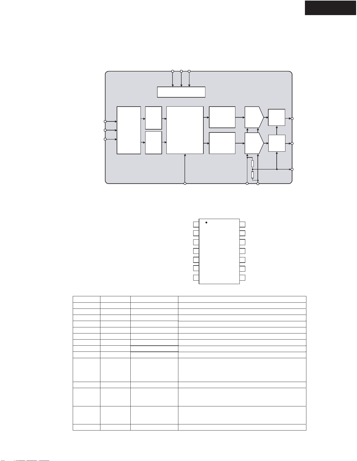
SYSTEM BLOCK DIAGRAM
A sampling system block diagram for the ES6629 Vibratto-II DVD
player board design is shown in Figure 2.
DVD/CD
SV-SP302
OPU
ES6603
RF Amp
8/16-MB
DRAM
EEPROM
ROM/Flash
Motor
Motor Driver
ES6629
Vibratto-II
Video
Audio DAC
Audio ADC
S/PDIF
VFD Driver
Figure 2 ES6629 Vibratto-II System Block Diagram
T
V Display
Speakers
Microphone In
A/V Receiver
VFD Panel
IR Remote
Page 40

IC BLOCK DIAGRAM/ TERMINAL DESCRIPTION
IC9 : HY57V641620HG D RAM-(1)
PIN CONFIGURATION
DV-SP302
VDD
DQ0
VDDQ
DQ1
DQ2
VSSQ
DQ3
DQ4
VDDQ
DQ5
DQ6
VSSQ
DQ7
VDD
LDQM
/WE
/CAS
/RAS
/CS
BA0
BA1
A10/AP
A0
A1
A2
A3
VDD
1
2
3
4
5
6
7
8
9
10
11
12
13
14
15
16
17
18
19
20
21
22
23
24
25
26
27
54pin TSOP II
400mil x 875mil
0.8mm pin pitch
54
53
52
51
50
49
48
47
46
45
44
43
42
41
40
39
38
37
36
35
34
33
32
31
30
29
28
VSS
DQ15
V SSQ
DQ14
DQ13
V DDQ
DQ12
DQ11
V SSQ
DQ10
DQ9
V DDQ
DQ8
VSS
NC
UDQM
CLK
CKE
NC
A11
A9
A8
A7
A6
A5
A4
VSS
PIN DESCRIPTION
PIN PIN NAME DESCRIPTION
CLK Clock
CK E Clock Enable
CS Chip Select Enables or disables all inputs except CLK, CKE and DQM
BA0,BA1 Bank Address
A0 ~ A11 Address
RAS, CAS, W E
LDQM, UDQM Data Input/Output Mask Controls output buffers in read mode and masks input data in write mode
DQ0 ~ DQ15 Data Input/Output Multiplexed data input / output pin
V
DD /VSS Power Supply/Ground Power supply for internal circuits and input buffers
V DDQ/V SSQ Data Output Power/Ground Power supply for output buffers
NC No Connection No connection
Row Address Strobe,
Column Address Strobe,
Write Enable
The system clock input. All other inputs are registered to the SDRAM on the
rising edge of CLK
Controls internal clock signal and when deactivated, the SDRAM will be one
of the states among power down, suspend or self refresh
Selects bank to be activated during R AS activity
Selects bank to be read/written during C AS activity
Row Address : RA0 ~ RA11, Column Address : CA0 ~ CA7
Auto-precharge flag : A10
RAS, CAS and WE define the operation
Refer function truth table for details
Page 41

IC BLOCK DIAGRAM/ TERMINAL DESCRIPTION
IC9 : HY57V641620HG D RAM-(2)
FUNCTIONAL BLOCK DIAGRAM
DV-SP302
Self refresh logic
& timer
CLK
CKE
CS
RAS
CAS
WE
UDQM
LDQM
Row active
State Machine
refresh
Column
Active
Internal Row
counter
Row
Pre
Decoders
Column
Pre
Decoders
1Mx16 Bank 3
X decoders
1Mx16 Bank 2
X decoders
X decoders
1Mx16 Bank 1
1Mx16 Bank 0
X decoders
Memory
Y decoders
Cell
Array
Sense AMP & I/O Gate
I/O Buffer & Logic
DQ0
DQ1
DQ14
DQ15
A0
A1
A11
BA0
BA1
Bank Select
Address
Address buffers
Registers
Mode Registers
Column Add
Counter
Burst
Counter
CAS Latency
Data Out Control
Pipe Line Control
Page 42

IC BLOCK DIAGRAM/ TERMINAL DESCRIPTION
IC8 : M24C02WMN6 EEPROM
Logic Diagram
V
CC
3
E0-E2 SDA
DV-SP302
SCL
WC
M24Cxx
V
SS
Signal Names
E0, E1, E2 Chip Enable Inputs
SDA Serial Data/Address Input/
Output
SCL Serial Clock
WC
V
CC
Write Control
Supply Voltage
V
SS
SO Connections
E0 V
E2
SS
Ground
M24Cxx
M24Cxx - W
M24Cxx - R
1
2
3
4
8
7
6
5
CC
WCE1
SCL
SDAV
Page 43

IC BLOCK DIAGRAM/ TERMINAL DESCRIPTION
IC12 : M29W800DT MEMORY FLASH
LOgic Diagram
Signal Names
DV-SP302
TSOP Connections
Page 44

IC BLOCK DIAGRAM/ TERMINAL DESCRIPTION
IC81 : M74HCU04 INVERTER IC
PIN CONNECTIONS
DV-SP302
PIN DESCRIPTION
Page 45
IC BLOCK DIAGRAM/ TERMINAL DESCRIPTION
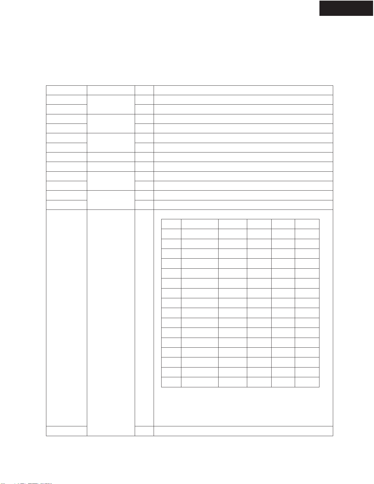
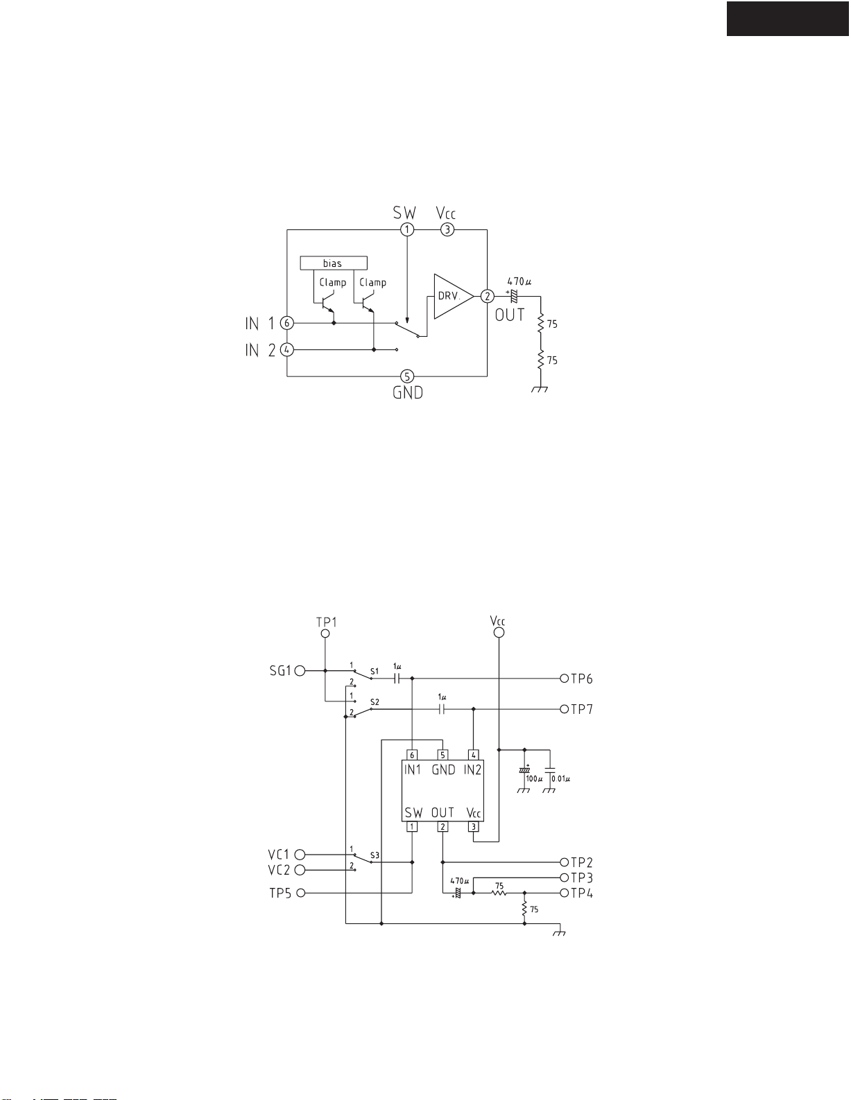
IC14 : MM1507 VIDEO SWITCH
Block Diagram
DV-SP302
Measuring circuit
Page 46
GND
VOUTR
CAP
NC
BCKIN
LRCIN
DIN
10
14
13
12
11
WM8761
VDD
VOUTL
MUTE
NC
DEEMPH
MCLK
FORMAT
IN
IO
CE
TE
OL
CE
TL
TR
MA
TA
OR
IN
IN
TE
MA
TA
OR
RS
OW
SS
ER
OW
PASS
ER
AP
AC
AC
61
IC BLOCK DIAGRAM/ TERMINAL DESCRIPTION
IC15 : WM8761 D/D Converter
DEEMPH
MUTE
BLOCK DIAGRAM
BCKIN
LRCRCIN
DIN
AUDUDIO
INTERFACE
MUTE
MUTE
FORMAT
CONTROL
INTERFACE
DIGIGITAL F FILTERS
MODULATOR
MODULATOR
SIGMA
DELTA
SIGMA
DELTA
DV-SP302
WM8761
LOW
DAC
DAC
PAPASS
FILTER
LOW
PASS
FILTER
VOUTR
VOUTL
CAP
MCLK
VDD
PIN CONFIGURATION
LRCIN
DIN
BCKIN
NC
CAP
VOUTR
GND
1
2
3
WM8761
4
5
6
7
14
13
12
11
10
9
8
MCLK
FORMAT
DEEMPH
NC
MUTE
VOUTL
VDD
PIN DESCRIPTION
PIN NAME TYPE DESCRIPTION
1
2 DIN Digital input Serial audio data input
3 BCKIN Digital inpu t Bit clock input
4
5
6 VOUTR Analogue output Right channel DAC output
7
8 VDD Supply Positive supply
9 VOUTL Analogue output Left channel DAC output
10 MUTE
11 NC No connect No internal connection
12
13 FORMAT Digital input Data input format select, Internal pull up
14 MCLK Digital input Master clock input
LRCIN Digital input Sample rate clock input
NC No connect No internal connection
CAP Analogue output Analogue internal reference
GND Supply Negative supply
D
igital input Soft mute control, Internal pull down
High Impedance
High = Mute ON
Low = Mute OFF
DEEMP H D igital i nput De-emphasis select,
High = de-em phasis ON
Low = de-emphasis OFF
Low = 24-bit right justified or DSP ‘late’
High = 16-24-bit I
Automute
=
I
nternal pull up
2
S or DSP ‘early’
GND
Page 47
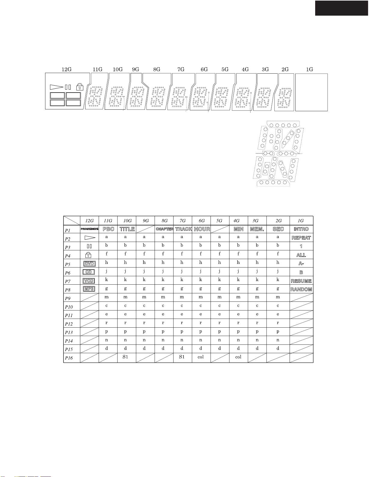
FL TUBE VIEW
INTRO
REPEAT
1 ALLA-B
RESUME
RANDOM
SEC
MEM.
MIN
HOUR
TRACK
CHAPTER
TITLE
PBC
PROGRESSIVE
DVD
VCD
CD
MP3
FL91 : HNV-12SM69T
GRID ASSIGNMENT
PROGRESSIVE
DVD
CD
VCD
MP3
PBC
TITLE
DV-SP302
TRACK
CHAPTER
S1
HOUR
COLS1
MIN
COL
g
e
MEM.
f
SEC
INTRO
REPEAT
1 ALLA-B
RESUME
RANDOM
a
h
j
b
k
m
r
n
p
c
ANODE CONNECTION
d
(2G - 11G)
Page 48

IC BLOCK DIAGRAM/ TERMINAL DESCRIPTION
IC91 : uPD16311 FL Driver-(1)
PIN CONFIGURATION
OSD
VSS
LED1
LED2
LED3
LED4
LED5
VDD
Grid1
Grid2
52
51
50
49
48
47
46
45
44
43
Grid3
42
Grid4
41
DV-SP302
Grid5
40
SW1
SW2
SW3
SW4
DOUT
DIN
IC
CLK
STB
KEY1
KEY2
KEY3
KEY4
10
11
12
13
1
2
3
4
5
6
7
8
9
14
15
16
17
18
19
20
21
22
23
24
25
26
VDD
39
38
37
36
35
34
33
32
31
30
29
28
27
Grid6
Grid7
Grid8
Seg20/Grid9
Seg19/Grid10
VEE
VDD
Seg18/Grid11
Seg17/Grid12
Seg16/Grid13
Seg15/Grid14
Seg14/Grid15
Seg13/Grid16
Seg1/KS1
Seg2/KS2
Seg3/KS3
Seg4/KS4
Seg5/KS5
Seg6/KS6
Seg7/KS7
Seg8/KS8
Seg9/KS9
Seg10/KS10
Seg11/KS11
Seg12/KS12
Page 49

IC BLOCK DIAGRAM/ TERMINAL DESCRIPTION
IC91 : uPD16311 FL Driver-(2)
BLOCK DIAGRAM
DV-SP302
DIN
DOUT
CLK
STB
Key
to
Key
SW1
to
SW
VDD
4
Command decoder
Dimming
circuit
Seg1
Serial I/F
Display memory
20 bit x 16 word
20
20-bit output latch
8
12
Segment driver
Seg12
Seg13/Grid16
R
OSD
1
4
4
4
4-bit latch
Timming generator
key scan
Key data memory (4 x 12)
5-bit latch
LED1 LED6
16
16-bit shift register
VDD VSS VEE
(+5V) (-30V)(0V)
8
Data selector
8
8
driver
Segment/ grid
Grid driver
Seg20/Grid9
Grid1
Grid8
Page 50

IC BLOCK DIAGRAM/ TERMINAL DESCRIPTION
IC91 : uPD16311 FL Driver-(3)
PIN FUNCTION
Pin No. Symbol Pin name Description
6
5
9
8
52
15 to 26
44 to 37
27 to 32
35 to 36
50 to 46
10 to 13
1 to 4
14, 33, 45
51
34
7
DIN
DOUT
STB
CLK
OSD
Seg1/KS1 to
Seg12/KS12
Grid1 to Grid6
Seg13/Grid16 to
Seg20/Grid9
LED1 to LED6
Key1 to Key4
SW1 to SW4
VDD
VSS
VEE
IC
Data input
Data output
Strobe
Clock input
Oscillator pin
High-voltage output
(segment)
High-voltage output (Grid)
High-voltage output
(segment/ grid)
LED output
Key data input
switch input
Logic power
Logic ground
Pull-down level
Internally connection
Inputs serial data at rising edge of shift clock,
starting from lower bit.
Outputs serial data at falling edge of shift clock, starting from
lower bit. This is N-ch open-drain output pin.
Initializes serial interface at rising or falling edge to make
uPD16311 waiting for reception of command. Data input
after STB has fallen is processed as command. While command
data is processed, current processing is stopped, and serial interface
is initializes. While STB is high, CLK is ignored.
Reads serial data at rising edge, and outputs data at falling edge.
Connect resistor for determining oscillation frequency to this pin.
Segment output pins (Dual function as key source).
Grid output pins.
Tease pins are selectable for segment or grid output.
CMOS output. +20 mA max..
Data input to these pins is latched at end of display cycle.
These pins constitute 4-bit general-purpose input port.
5 V = 10 %
connect this pin to GND of system.
VDD - 35 V max.
Be sure to leave this pin open (this pin is at VDD level).
DV-SP302
Page 51

UPGRADE FIRM WARE
Confirm the version of firmware.
1. Open a tray.
2. Press the "SEARCH DOWN" button 2 second at the unit and
"POWER" key on the remote controller.
Displayed on the FL tube like "1022". ex)
3. Turn off the power switch and power on, again.
Initializing
4. While display version of firmware, turn off a mechanical power switch.
Upgrade the firmware
1. Connect a video monitor to video out jack on the DV-SP302.
2. Turn on the power switch and standby switch on.
3. Setting the disc on the tray. (Down load firmware data disc)
4. Will start the Firm Ware updating.
Display repeat "ERASES" and "WRITE" on the monitor.
Will tray open after finish the updating.
Light up "STANDBY/ON" LED. = Complete the upgrade FW.
5. Turn off mechanical power switch.
6. Turn on the power switch again and take out the disc and close the tray.
1022= FW version 1.22
DV-SP302
Page 52
NOTE
Pack the unit that have been set the DVD mechanism
to initial mode (Push standby button so that set can
goes into standby mode. Pull out AC-cord (after
check power switch ON).
STEP 1 : LABEL FOR SET POSITION
DETAIL - CARD CERTIFICATE
Rear side
Front side
Apply to DV-SP302 CUR6P only
Record trier's name and data
before packing in card certificate.
Rear side
Changed packing location
For Rear panel
For Carton box
STEP 2 : KNOB POWER POSITION
STEP 3 : SET PACKING
3
Rear side
Bottom side
Rear side
Bottom side
STEP 4 : SET IN BOX
1
Stick in the card certificate
23
4
Front side
8
Stick in the middle position
on the front side wall
by double side tape
STEP 5 : AC CORD POSITION
Front side
OFF (NG)
ON OFF
POWER
ON (OK)
Knob power position : ON
Label Rating
Only DV-SP302(G) CUK3P
21
2
Rear panel
POS Label
PACKING PROCESURE
Page 53

6
7
5
10
Stick in the accessory
Left side
11
STEP 6 : PACKING IN ACCESSORIES
(PUT ON THE POLY BAG).
Attach tape to PE bag.
Battery
Detail view
20
12
13
14
15
16
17
Front side
11
Roll a PE bag and
attach tape to PE bag. (2 place)
19
18
Not apply to DV-SP302 CUR6P (CHINA VERSION ONLY)
Stick in the accessory
STEP 7 : LABEL FOR BOX POSITION
For Rear panel
Right side
Front
DV-SP302
DV-SP302
Page 54

NOTE
Pack the unit that have been set the DVD mechanism
to initial mode (Push standby button so that set can
goes into standby mode. Pull out AC-cord (after
check power switch ON).
STEP 1 : LABEL FOR SET POSITION
DETAIL - CARD CERTIFICATE
Rear side
Front side
Apply to DV-SP302 CUR6P only
Record trier's name and data
before packing in card certificate.
Rear side
Changed packing location
For Rear panel
For Carton box
STEP 2 : KNOB POWER POSITION
STEP 3 : SET PACKING
3
Rear side
Bottom side
Rear side
Bottom side
STEP 4 : SET IN BOX
1
Stick in the card certificate
23
4
6
7
5
Front side
8
Stick in the middle position
on the front side wall
by double side tape
STEP 5 : AC CORD POSITION
10
Front side
Stick in the accessory
Left side
11
STEP 6 : PACKING IN ACCESSORIES
(PUT ON THE POLY BAG).
Attach tape to PE bag.
Battery
Detail view
20
12
13
14
15
16
17
Front side
11
Roll a PE bag and
attach tape to PE bag. (2 place)
19
18
Not apply to DV-SP302 CUR6P (CHINA VERSION ONLY)
Stick in the accessory
STEP 7 : LABEL FOR BOX POSITION
For Rear panel
Right side
Front
DV-SP302
OFF (NG)
ON OFF
POWER
ON (OK)
Knob power position : ON
Label Rating
Only DV-SP302(G) CUK3P
21
2
Rear panel
POS Label
DV-SP302
PACKING PROCESURE
Page 55

PARTS LIST
55932710
I
l
CUR6P
(G)
P
1
d
0
PACKING PARTS LIST
Qt'y
NO. PART NO. PART NAME DESTINATION DESCRIPTION
55832660 POS Label <B CDD1N>
55932730 POS Label
2 LABEL POS
55932750 POS Label
55932760 POS Label
55932740 POS Label
<S CDD1N>
<B CUA4P>
<S CUA4P>
<G CUT3P> <G CUK3P> <G CUR6P>
3 55169520 Sheet
4 5568332A Pad L
5 5568331A Pad R
6 20194780 Cable tie
7 55259730 PE Bag
8 5520874A Cushion
5583263A Carton box
5593265A Carton box
5593266A Carton box
10
5593267A Carton box
5593268A Carton box
5593269A Carton box
5593270A Carton box
<B CDD1N>
<S CDD1N>
<B CUA4P>
<S CUA4P>
<G CUT3P>
<G CUK3P>
<G CUR6P>
11 55170650 PE Bag
12 55176530 Audio/ Video cable
13 55186190 Coaxial cable
14 55743520 RI cable
15 55236070 AC Adapter
<B CUA4P> <S CUA4P> <G CUT3P>
16 5502022A Battery
17 55167260 Remote controller
55832640 Instruction manual
55932720 Instruction manual
nstruction manua
19 55511980 Warranty car
<G CUT3P>
<G
<B CDD1N> <SCDD1N>
>
20 55030950 PE Bag
AC PRI LABEL POS DV-SP302(B) CDD1N
AC PRI LABEL POS DV-SP302(S) CDD1N
AC PRI LABEL POS DV-SP302(B) CUA4P
AC PRI LABEL POS DV-SP302(S) CUA4P
AC PRI LABEL POS DV-SP302(G) CUT3P
AC RAW BAG SHEET EPE TAV5100 820MM X 820MM
AC CPL ENDCAP CUSHION LEFT DV-SP301 UDD
AC CPL ENDCAP CUSHION RIGHT DV-SP301 UDD
CABLE-FIX CABLE-TIE THE FITMOS PLASTIC 0 0
AC CPL BAG POLY PE T0.05 350MM X 115MM
MAT-PKG CUSHION 80.0MM X 35.0MM 0 0
AC CARTON DV-SP302(B) CDD1N DW-2
AC CARTON DV-SP302(S) CDD1N DW-2
AC CARTON DV-SP302(B) CUA4P DW-2
AC CARTON DV-SP302(S) CUA4P DW-2
AC CARTON DV-SP302(G) CUT3P DW-2
AC CARTON DV-SP302(G) CUK3P DW-2
AC CARTON DV-SP302(G) CUR6P DW-2
AC CPL BAG RCA 260MM X 410MM
WIRE-CABSP AUDIO-CABLE STEREO 1500MM BK 0 A0
WIRE-CABSP AUDIO-CABLE MONO 1000MM OG 0 0
WIRE-CABSP AUDIO-CABLE MONO 800MM BU 0 A0
CON ADPTR PLUG AC ADAPTOR -BATNCALK 1.5V AAA 1.15 AH
EPR RCT REMOCON DV-S353 OEM -- W/O BATTERY -AC BOOK INSTR DV-SP302(B) CDD1N
AC BOOK INSTR DV-SP302(G) CUT3P
AC BOOK INSTR DV-SP302
AC PRI CARD WARRANTY ONKYO DV-CP50
AC CPL BAG PE 45MM X 80MM
CUR6
(B)CDD1N (S)CDD1N (B)CUA4P (S)CUA4P (G)CUT3P (G)CUK3P (G)CUR6P
1
1
1
1
111
1111111
1111111
1111111
1111111
1111111
1111111
1
1
1
1
1
1
1
2222222
1111111
1111111
1111111
111
2222222
1111111
111111
1
11
1111111
REMARK
CARTON BOX
MANUAL18
Page 56
PARTS LIST
P
EXPLODED VIEW
PART NO.
No
1 55209110 Finger PIN-STRIP 0.0MM 1 -- U FINGER STRIP DVD10 0 0 1.0 1.0 1.0 1.0 1.0 1.0 1.0
2 55221140 Shield cover AC RAW SHIELD COVER SENSOR DV-C503 1.0 1.0 1.0 1.0 1.0 1.0 1.0
3 55186710 Facet AC MLD CRYSTAL ST/BY DV-C503 1.0 1.0 1.0 1.0 1.0 1.0 1.0
55830650 Front display board <B CDD1N>
55931380 Front display board <B CUA4P>
55931390 Front display board <S CDD1N>
U4
55931400 Front display board <S CUA4P>
55931410 Front display board <G CUT3P>
55931420 Front display board <G CUK3P>
55931430 Front display board <G CUR6P>
55830650-1 FL tube board <B CDD1N>
55931380-1 FL tube board <B CUA4P>
55931390-1 FL tube board <S CDD1N>
U4-1
55931400-1 FL tube board <S CUA4P>
55931410-1 FL tube board <G CUT3P>
55931420-1 FL tube board <G CUK3P>
55931430-1 FL tube board <G CUR6P>
55830650-2 Key switch board <B CDD1N>
55931380-2 Key switch board <B CUA4P>
55931390-2 Key switch board <S CDD1N>
U4-2
55931400-2 Key switch board <S CUA4P>
55931410-2 Key switch board <G CUT3P>
55931420-2 Key switch board <G CUK3P>
55931430-2 Key switch board <G CUR6P>
55830650-3 Standby switch board <B CDD1N>
55931380-3 Standby switch board <B CUA4P>
55931390-3 Standby switch board <S CDD1N>
U4-3
55931400-3 Standby switch board <S CUA4P>
55931410-3 Standby switch board <G CUT3P>
55931420-3 Standby switch board <G CUK3P>
55931430-3 Standby switch board <G CUR6P>
55830650-4 Remote sensor board <B CDD1N>
55931380-4 Remote sensor board <B CUA4P>
55931390-4 Remote sensor board <S CDD1N>
U4-4
55931400-4 Remote sensor board <S CUA4P>
55931410-4 Remote sensor board
55931420-4 Remote sensor board <G CUK3P>
55931430-4 Remote sensor board <G CUR6P>
55830660 DVD Main board assy <B CDD1N> AC EMBD IMA MAIN BD DV-SP302(B) CDD1N
55931690 DVD Main board assy <S CDD1N> AC EMBD IMA MAIN BD DV-SP302(S) CDD1N
55931680 DVD Main board assy <B CUA4P> AC EMBD IMA MAIN BD DV-SP302(B) CUA4P
U20
55931700 DVD Main board assy <S CUA4P> AC EMBD IMA MAIN BD DV-SP302(S) CUA4P
55931710 DVD Main board assy <G CUT3P> AC EMBD IMA MAIN BD DV-SP302(G) CUT3P
PART NAME DST/ COLOR
<G CUT3P>
DESCRIPTION
AC EMBD IMA FRONT BD DV-SP302(B) CDD1N 1.0
AC EMBD IMA FRONT BD DV-SP302(B) CUA4P 1.0
AC EMBD IMA FRONT BD DV-SP302(S) CDD1N 1.0
AC EMBD IMA FRONT BD DV-SP302(S) CUA4P 1.0
AC EMBD IMA FRONT BD DV-SP302(G) CUT3P 1.0
AC EMBD IMA FRONT BD DV-SP302(G) CUK3P 1.0
AC EMBD IMA FRONT BD DV-SP302(G) CUR6P 1.0
Included U4 (Front display board)
Included U4 (Front display board)
Included U4 (Front display board)
Included U4 (Front display board)
(B)CDD1N (S)CDD1N (B)CUA4P
1.0
1.0
1.0
1.0
1.0
1.0
1.0
1.0
1.0
1.0
Qt'y
S)CUA4PG)CUT3PG)CUK3PG)CUR6
1.0
1.0
1.0
1.0
1.0
1.0
1.0
1.0
1.0
1.0
1.0
1.0
1.0
1.0
1.0
1.0
1.0
1.0
1.0
REMARK
NSP
1.0
1.0
1.0
1.0
MAIN BD
Page 57

55931720 DVD Main board assy <G CUK3P> AC EMBD IMA MAIN BD DV-SP302(G) CUK3P
1.0
55931730 DVD Main board assy <G CUR6P> AC EMBD IMA MAIN BD DV-SP302(G) CUR6P
55830670 Output terminal board assy <B CDD1N> AC EMBD IMA OUT BD DV-SP302(B) CDD1N
55931930 Output terminal board assy <S CDD1N> AC EMBD IMA OUT BD DV-SP302(S) CDD1N
55931920 Output terminal board assy <B CUA4P> AC EMBD IMA OUT BD DV-SP302(B) CUA4P
U21
55931940 Output terminal board assy <S CUA4P> AC EMBD IMA OUT BD DV-SP302(S) CUA4P
55931950 Output terminal board assy <G CUT3P> AC EMBD IMA OUT BD DV-SP302(G) CUT3P
55931960 Output terminal board assy <G CUK3P> AC EMBD IMA OUT BD DV-SP302(G) CUK3P
1.0
1.0
1.0
1.0
1.0
1.0
55931970 Output terminal board assy <G CUR6P> AC EMBD IMA OUT BD DV-SP302(G) CUR6P
55678210 Button Standby
5
55688530 Button Standby
55688540 Button Standby
55832550 Front panel
55932560 Front panel
6
55932570 Front panel
55932580 Front panel
55932590 Front panel
55186750 Badge LOGO
7
55688330 Badge LOGO
55832570 Door
8
55932600 Door
55932610 Door
55384980 Badge
9
55688340 Badge
55678230 Clear plate
10
55688570 Clear plate
55832590 Bracket Mecha.
11
55678220 Button 6 key
12
55688550 Button 6 key
55688560 Button 6 key
55678190 Button Open/ Close
13
55688510 Button Open/ Close
55688520 Button Open/ Close
<B>
<S>
<G>
<B CDD1N>
<S CDD1N>
<B CUA4P>
<S CUA4P>
<G CUT3P>
<B>
<S> <G>
<B>
<S>
<G>
<B>
<S> <G>
<B>
<S> <G>
<B>
<S>
<G>
<B>
<S>
<G>
AC MLD BUTTON STANDBY DV-SP301 BK HIPS 1.0 1.0
AC DEC BUTTON STANDBY DV-SP301(S) UDD1N HIPS 1.0 1.0
AC DEC BUTTON STANDBY DV-SP301(G) UUT3P HIPS 1.0 1.0 1.0
AC DEC CABINET PANEL FRONT DV-SP302(B) CDD1N 1.0
AC DEC CABINET PANEL FRONT DV-SP302(S) CDD1N 1.0
AC DEC CABINET PANEL FRONT DV-SP302(B) CUA4P 1.0
AC DEC CABINET PANEL FRONT DV-SP302(S) CUA4P 1.0
AC DEC CABINET PANEL FRONT DV-SP302(G) CUT3P 1.0 1.0 1.0
AC CPL PLATE LOGO-ONKYO DV-C503 1.0 1.0
AC CPL PLATE LOGO-ONKYO DV-SP301(S),(G) 1.0 1.0 1.0 1.0 1.0
AC DEC DOOR TRAY DV-SP302(B) CDD1N BK 1.0 1.0
AC DEC DOOR TRAY DV-SP302(S) CDD1N SI01TH 1.0 1.0
AC DEC DOOR TRAY DV-SP302(G) CUT3P GD01TH 1.0 1.0 1.0
AC CPL PLATE BADGE DVD DPC5.3 1.0 1.0
AC CPL PLATE BADGE DVD DV-SP301(S),(G) 1.0 1.0 1.0 1.0 1.0
AC MLD CRYSTAL WINDOW DISPLAY DV-SP301 1.0 1.0
AC MLD CRYSTAL WINDOW DISPLAY DV-SP301(S),(G) 1.0 1.0 1.0 1.0 1.0
AC PUN BRACKET MECHA DV-SP302 SECC 1.0T 1.0 1.0 1.0 1.0 1.0 1.0 1.0
AC MLD BUTTON 6KEY DV-SP301 BK HIPS 1.0 1.0
AC DEC BUTTON 6KEY DV-SP301(S) UDD1N HIPS 1.0 1.0
AC DEC BUTTON 6KEY DV-SP301(G) UUT3P HIPS 1.0 1.0 1.0
AC MLD BUTTON OPEN/CLOSE DV-SP301 BK HIPS 1.0 1.0
AC DEC BUTTON OPEN/CLOSE DV-SP301(S) UDD1N HIPS 1.0 1.0
AC DEC BUTTON OPEN/CLOSE DV-SP301(G) UUT3P HIPS 1.0 1.0 1.0
14 55929750 FL tube DISPLAY HNV-12SM69T DV-SP302(ONKYO) 1.0 1.0 1.0 1.0 1.0 1.0 1.0
55832580 Holder FL tube
15
55914040 Plate
16
AC MLD HOLDER VFD DV-SP302 1.0 1.0 1.0 1.0 1.0 1.0 1.0
AC PUN PLATE GUIDE DV-SP302 1.0 1.0 1.0 1.0 1.0 1.0 1.0
17 55141370 Rubber Foot AC FOOT RUBBER ROUND 3.0MM 25.0MM JIS 60 Y DIA 4.0 4.0 4.0 4.0 4.0 4.0 4.0
5512512A Foot
18
55832480 Chassis
19
55832490 Rear panel
55932620 Rear panel
28
55932630 Rear panel
55932640 Rear panel
29 55125180 Bushing
55190780 Power cord
55190790 Power cord
30
55968210 Power cord
55328430 Power cord
<B S> <CDD1N>
<B> <CUA4P>
<G> <CUT3P> <CUK3P>
<G> <CUR6P>
!
<CDD1N> !
<CUA4P> <CUT3P> !
<CUK3P> !
<CUR6P> !
AC RAW FOOT REAR ROUND 12.5MM 50MM 4.0 4.0 4.0 4.0 4.0 4.0 4.0
AC CPL CABINET CHASSIS MAIN DV-SP302 1.0 1.0 1.0 1.0 1.0 1.0 1.0
AC CPL REAR PANEL DV-SP302(B) CDD1N 1.0 1.0
AC CPL REAR PANEL DV-SP302(B) CUA4P 1.0 1.0
AC CPL REAR PANEL DV-SP302(G) CUT3P 1.0 1.0
AC CPL REAR PANEL DV-SP302(G) CUR6P 1.0
AC MLD CLAMP AC CORD RT2280/RT2250(PAV5007/PAV5005) 1.0 1.0 1.0 1.0 1.0 1.0 1.0
WIRE-MCRDM 0.75MM2 2200MM BK US LMPS0242-O 1.0 1.0
WIRE-MCRDM 0.75MM2 2200MM BK EU H03VVH2-F 1.0 1.0 1.0
WIRE-MCRDM 0.75MM2 2200MM BK KS 1.0
WIRE-MCRDM 0.75MM2 1830MM BK CCEE POWER CORD 1.0
1.0
OUT BD
1.0
BUTTON STANDBY
PANEL FRONT
BADGE ONKYO
DOOR TRAY
BADGE DVD
WINDOW DSP
BUTTON 6KEY
BUTTON OPEN/CLOSE
REAR PANEL
AC POWER CORD
Page 58

31 55934240 Power supply unit
55678120 Knob
32
55688410 Knob
55688420 Knob
55683400 Top cover
33
55688580 Top cover
55688590 Top cover
55896680 DVD Loader mechanism
34
!
<B CDD1N> <B CUA4P>
<S CDD1N> <S CUA4P>
<G >
<B>
<S>
<G>
AD ASY SMPS KSP118F-1102005-0 1.0 1.0 1.0 1.0 1.0 1.0 1.0
AC MLD KNOB POWER DV-SP301 BK 1.0 1.0
AC DEC KNOB POWER DV-SP301(S) UDD1N 1.0 1.0
AC DEC KNOB POWER DV-SP301(G) UUT3P 1.0 1.0 1.0
AC PUN COVER TOP DV-SP301 BK -- -- 1.0 1.0
AC PUN COVER TOP DV-SP301(S) UDD1N PCM 0.7T SI01TH 1.0 1.0
AC PUN COVER TOP DV-SP301(G) UUS4P PCM 0.7T GD01TH 1.0 1.0 1.0
AC MSA ASY WXD-8610(2) DVD LOADER 1.0 1.0 1.0 1.0 1.0 1.0 1.0
35 55926240 Frame AC PUN BRACKET FRAME MECHA DV-SP302 SECC 1.0T 1.0 1.0 1.0 1.0 1.0 1.0 1.0
36 5516498A Spacer AC MLD BRACKET SPACE PCB BK PLASTIC 3.0 3.0 3.0 3.0 3.0 3.0 3.0
55943700 Traverse mechanism
37
55768220 Plate
38
55179040 Wire
39
55212250 Cable clamp CABLE-FIX CLAMP WIRE UL DENNISON 0 0
40
AC MSA ASY PICK-UP TRAVERSE CMS-S71SG6T 1.0 1.0 1.0 1.0 1.0 1.0 1.0
AC PUN PLATE EARTH DV-SP301 1.0 1.0 1.0 1.0 1.0
WIRECONASY UNIQUE 1P 140MM UL1007 PVC DISCRETE 24 1 1.0 1.0 1.0 1.0 1.0
2.0 2.0 2.0 2.0 2.0 2.0 2.0
S1 55127290 Screw SCREW-ST 3MM 18MM JIS B 1122 J80600031810 53 0 0 3.0 3.0 3.0 3.0 3.0 3.0 3.0
S2 55164800 Screw SCREW 3MM 8MM DIN963 62 2182 B7 15.0 15.0 15.0 15.0 15.0 15.0 15.0
55127070 Screw SCREW-ST 3MM 10MM JIS B 1122 J5636140010X 19 0 0 13.0 6.0 13.0 6.0 6.0 6.0 6.0
S3
55215970 Screw SCREW-ST 3MM 8MM JIS B 1122 53 0 0 7.0 7.0 7.0 7.0 7.0
S4 55135460 Screw SCREW-SPEC 3MM 10MM JIS J90720301080 27 0 0 11.0 11.0 11.0 11.0 11.0 11.0 11.0
S5 20363340 Screw SCREW-ST 2.6MM 8MM JIS B 1122 53 0 0 14.0 14.0 14.0 14.0 14.0 14.0 14.0
S6 55127180 Screw SCREW-ST 3MM 8MM JIS B 1122 25 0 0 2.0 2.0 2.0 2.0 2.0 2.0 2.0
55127280 Screw SCREW-ST 3MM 6MM JIS B 1122 25 0 0 2.0 2.0
S7
55127120 Screw SCREW-ST 3MM 8MM JIS B 1122 J5636140040X 53 0 0 2.0 2.0 2.0 2.0 2.0
S8 55546030 Screw SCREW-ST 3MM 6MM SAM 53 0 A4 1.0 1.0 1.0 1.0 1.0 1.0 1.0
KNOB POWER
COVER TOP
NOTE:
<B>:
<S>:
<G>:
<CUD1N>:
<CUA4P>:
<CUT3P>:
<CUK3P>:
Black color model
Silver color model
Golden color model
North American model
Australian model
Asia model
Korean model
Page 59

DV-SP302(B) UDD1N PART LIST
T
PC BOARD PARTS LIS
FRONT DISPLAY BOARD DV-SP302
CIRCUIT NO. PART NAME PART NO. DESCRIPTION
0050 Holder 55832580 front FL tube
CN61 Socket AS 55180520 5P 220mm, 2.0mm
CN62 Socket AS 55951950 9P 130mm, 2.0mm
CN63 Socket AS 55158680 2P 80mm, 2.0mm
CN71 Socket AS 55951960 12P 100mm, 2.0mm
CN72 Socket AS 55951970 6P 90mm, 2.0mm
CP64 Connector 55078520 CONN 2.0MM 2 MA R NAT LW2003P02 0 0
FG60 Finger 55209110 PIN-STRIP 0.0MM 1 -- U FINGER STRIP DVD10 0 0
FG63 Finger plate 55178960 AC SPRING PLATE SPRING GND C5212 0.2T AVR520
FL91 FL tube 55929750 DISPLAY HNV-12SM69T DV-SP302(ONKYO)
LD61 LED 55125510 D-LEM LTL-1CHE RD RND 3.0 DIFU 5.6CD
RM61 Remote sensor 55193920 IC-REMOTE NJL64H380A RECEIVER 38KHZ
C901 Capacitor ceramic 11059320 CCCFMIN 1N0F +10% -10% 50.0V X7R
C902 Capacitor ceramic 20251250 CCCFMIN 47N0F +10% -10% 50.0V X7R
C904 Capacitor ceramic 20267290 CCCFMIN 100N0F +80% -20% 50.0V Y5V
C905 Capacitor ceramic 20267290 CCCFMIN 100N0F +80% -20% 50.0V Y5V
C916 Capacitor ceramic 30938700 CCCFMIN 68P0F +5% -5% 50.0V NP0
C917 Capacitor ceramic 30938700 CCCFMIN 68P0F +5% -5% 50.0V NP0
C918 Capacitor ceramic 30938700 CCCFMIN 68P0F +5% -5% 50.0V NP0
C919 Capacitor ceramic 30938700 CCCFMIN 68P0F +5% -5% 50.0V NP0
C920 Capacitor ceramic 30938700 CCCFMIN 68P0F +5% -5% 50.0V NP0
C921 Capacitor ceramic 30938700 CCCFMIN 68P0F +5% -5% 50.0V NP0
C922 Capacitor ceramic 30938700 CCCFMIN 68P0F +5% -5% 50.0V NP0
C923 Capacitor ceramic 30938700 CCCFMIN 68P0F +5% -5% 50.0V NP0
C924 Capacitor ceramic 30938700 CCCFMIN 68P0F +5% -5% 50.0V NP0
C925 Capacitor ceramic 30938700 CCCFMIN 68P0F +5% -5% 50.0V NP0
C926 Capacitor ceramic 30938700 CCCFMIN 68P0F +5% -5% 50.0V NP0
C927 Capacitor ceramic 30938700 CCCFMIN 68P0F +5% -5% 50.0V NP0
D601 Diode 20496510 D-SLP 1SS355 35.0V 225MI0A
IC91 IC 20920150 IC-DISPLAY UPD16311GC-AB6 HIGH VOLTAGE DRIVER
Q601 Trnsistor 55051240 TR-SSD KRC107S N 10K0 OHM 47K0 OHM
R606 Resistor 15268430 RMGCFMIN 1R0 OHM +5% 100MI0W
R607 Resistor 11066420 RMGCFMIN 390R0 OHM +5% 100MI0W
R608 Resistor 30944310 RMGCFMIN 4K7 OHM +5% 100MI0W
R609 Resistor 70434200 RMGCFMIN 100R0 OHM +5% 100MI0W
R701 Resistor 50886610 RMGCFMIN 10K0 OHM +5% 100MI0W
R702 Resistor 50886610 RMGCFMIN 10K0 OHM +5% 100MI0W
R703 Resistor 50886610 RMGCFMIN 10K0 OHM +5% 100MI0W
R704 Resistor 50886610 RMGCFMIN 10K0 OHM +5% 100MI0W
R901 Resistor 50886610 RMGCFMIN 10K0 OHM +5% 100MI0W
R902 Resistor 50886610 RMGCFMIN 10K0 OHM +5% 100MI0W
R903 Resistor 50886610 RMGCFMIN 10K0 OHM +5% 100MI0W
R904 Resistor 50886610 RMGCFMIN 10K0 OHM +5% 100MI0W
R906 Resistor 80440510 RMGCFMIN 0 OHM +0% 100MI0W
R909 Resistor 50886620 RMGCFMIN 39K0 OHM +5% 100MI0W
R910 Resistor 80440510 RMGCFMIN 0 OHM +0% 100MI0W
R919 Resistor 80440510 RMGCFMIN 0 OHM +0% 100MI0W
R931 Resistor 11066510 RMGCFMIN 120K0 OHM +5% 100MI0W
R932 Resistor 11066510 RMGCFMIN 120K0 OHM +5% 100MI0W
C601 Capacitor Electric 15002130 CE 10U0F +20% 16.0V 85C
SW71 Tact switch 55145270 SWITACT VERTICAL F/B 50MI0A 12.0V 500MI0OHM 1T 1P
SW72 Tact switch 55145270 SWITACT VERTICAL F/B 50MI0A 12.0V 500MI0OHM 1T 1P
SW73 Tact switch 55145270 SWITACT VERTICAL F/B 50MI0A 12.0V 500MI0OHM 1T 1P
SW74 Tact switch 55145270 SWITACT VERTICAL F/B 50MI0A 12.0V 500MI0OHM 1T 1P
SW75 Tact switch 55145270 SWITACT VERTICAL F/B 50MI0A 12.0V 500MI0OHM 1T 1P
SW76 Tact switch 55145270 SWITACT VERTICAL F/B 50MI0A 12.0V 500MI0OHM 1T 1P
SW77 Tact switch 55145270 SWITACT VERTICAL F/B 50MI0A 12.0V 500MI0OHM 1T 1P
SW78 Tact switch 55145270 SWITACT VERTICAL F/B 50MI0A 12.0V 500MI0OHM 1T 1P
D901 Diode 70436540 D-SLP 1N4148 100.0V 150E-3A
D902 Diode 70436540 D-SLP 1N4148 100.0V 150E-3A
1 / 10
Page 60

DV-SP302(B) UDD1N PART LIST
D903 Diode 70436540 D-SLP 1N4148 100.0V 150E-3A
R601 Resistor 30939360 RCF 10R0 OHM +5% 250MI0W
R602 Resistor 30939370 RCF 15R0 OHM +5% 250MI0W
R603 Resistor 30939370 RCF 15R0 OHM +5% 250MI0W
R604 Resistor 30939370 RCF 15R0 OHM +5% 250MI0W
R605 Resistor 30939370 RCF 15R0 OHM +5% 250MI0W
MAIN BOARD DV-SP302
CIRCUIT NO. PART NAME PART NO. DESCRIPTION
C6 Capacitor 55126060 CC 470P0F +10% -10% 50.0V 2B4
CC1A Socket AS 55933000 6P 80mm, 2.0mm
CC4A Socket AS 55933010 5P 80mm, 2.0mm
CC5A FFC 55946320 FFC-JUMPER 24X 0.5MM 190MM D TYPE
CD49 Capacitor 10071220 CE 100U0F +20% 10.0V 85C 10124720
CD50 Capacitor 10071220 CE 100U0F +20% 10.0V 85C 10124720
CD57 Capacitor 10071220 CE 100U0F +20% 10.0V 85C 10124720
CD58 Capacitor 80434330 CE 100U0F +20% 10.0V 85C
CD59 Capacitor 80434330 CE 100U0F +20% 10.0V 85C
CD60 Capacitor 80434330 CE 100U0F +20% 10.0V 85C
CD61 Capacitor 80434330 CE 100U0F +20% 10.0V 85C
CD63 Capacitor 20267830 CE 47U0F +20% 16.0V 85C 20251640
CD64 Capacitor 80434330 CE 100U0F +20% 10.0V 85C
CD66 Capacitor 20252650 CE 220U0F +20% 16.0V 85C
CN2 Socket AS 55932990 WIRECONASY 07305H 7P 300MM UL1007 RIBBON 22 1
CP1 Socket AS 55123330 CONN 2.0MM 6 MA ST NAT LW2002P06 0 0
CP2 Socket AS 55123380 CONN 2.0MM 15 MA ST NAT LW2002P15 0 0
CP3 Socket AS 55123330 CONN 2.0MM 6 MA ST NAT LW2002P06 0 0
CP4 Socket AS 55123320 CONN 2.0MM 5 MA ST NAT LW2002P05 0 0
CP8 Socket AS 55090070 CONN 2.0MM 2 MA ST NAT LW2002P0200T 0 0
D11 Diode silicon 20415060 D-SR 1N4004 400.0V 1.0A
D12 Diode silicon 20415060 D-SR 1N4004 400.0V 1.0A
GND1 Terminal 55135980 TERMLUG GND
Y1 Oscillator 55827880 FILQZ 27M0 HZ +30 PPM 40.0 OHM 20P0 F
B10 Capacitor 20288040 CCCFMIC 100N0F +80% -20% 16.0V Y5V
B11 Capacitor 20288040 CCCFMIC 100N0F +80% -20% 16.0V Y5V
B12 Capacitor 20288040 CCCFMIC 100N0F +80% -20% 16.0V Y5V
B15 Capacitor 20288040 CCCFMIC 100N0F +80% -20% 16.0V Y5V
B24 Capacitor 20288040 CCCFMIC 100N0F +80% -20% 16.0V Y5V
B25 Capacitor 20288040 CCCFMIC 100N0F +80% -20% 16.0V Y5V
B26 Capacitor 20288040 CCCFMIC 100N0F +80% -20% 16.0V Y5V
B27 Capacitor 20288040 CCCFMIC 100N0F +80% -20% 16.0V Y5V
B28 Capacitor 20288040 CCCFMIC 100N0F +80% -20% 16.0V Y5V
B29 Capacitor 20288040 CCCFMIC 100N0F +80% -20% 16.0V Y5V
B30 Capacitor 20288040 CCCFMIC 100N0F +80% -20% 16.0V Y5V
B31 Capacitor 20288040 CCCFMIC 100N0F +80% -20% 16.0V Y5V
B32 Capacitor 20288040 CCCFMIC 100N0F +80% -20% 16.0V Y5V
B33 Capacitor 20288040 CCCFMIC 100N0F +80% -20% 16.0V Y5V
B36 Capacitor 20288040 CCCFMIC 100N0F +80% -20% 16.0V Y5V
B37 Capacitor 20288040 CCCFMIC 100N0F +80% -20% 16.0V Y5V
B38 Capacitor 20288040 CCCFMIC 100N0F +80% -20% 16.0V Y5V
B39 Capacitor 20288040 CCCFMIC 100N0F +80% -20% 16.0V Y5V
B40 Capacitor 20288040 CCCFMIC 100N0F +80% -20% 16.0V Y5V
B41 Capacitor 20288040 CCCFMIC 100N0F +80% -20% 16.0V Y5V
B42 Capacitor 20288040 CCCFMIC 100N0F +80% -20% 16.0V Y5V
B46 Capacitor 20288040 CCCFMIC 100N0F +80% -20% 16.0V Y5V
B9 Capacitor 20288040 CCCFMIC 100N0F +80% -20% 16.0V Y5V
C1 Capacitor 20506680 CCCFMIC 470P0F +5% -5% 50.0V NP0
C106 Capacitor 20288040 CCCFMIC 100N0F +80% -20% 16.0V Y5V
C107 Capacitor 20288040 CCCFMIC 100N0F +80% -20% 16.0V Y5V
C109 Capacitor 20288040 CCCFMIC 100N0F +80% -20% 16.0V Y5V
C11 Capacitor 20506680 CCCFMIC 470P0F +5% -5% 50.0V NP0
C19 Capacitor 20288040 CCCFMIC 100N0F +80% -20% 16.0V Y5V
C21 Capacitor 20288040 CCCFMIC 100N0F +80% -20% 16.0V Y5V
C22 Capacitor 20288040 CCCFMIC 100N0F +80% -20% 16.0V Y5V
2 / 10
Page 61

DV-SP302(B) UDD1N PART LIST
C27 Capacitor 20506540 CCCFMIC 10P0F +0P5F -0P5F 50.0V NP0
C28 Capacitor 20506540 CCCFMIC 10P0F +0P5F -0P5F 50.0V NP0
C29 Capacitor 20506540 CCCFMIC 10P0F +0P5F -0P5F 50.0V NP0
C3 Capacitor 20506680 CCCFMIC 470P0F +5% -5% 50.0V NP0
C30 Capacitor 20506540 CCCFMIC 10P0F +0P5F -0P5F 50.0V NP0
C5 Capacitor 20506680 CCCFMIC 470P0F +5% -5% 50.0V NP0
C558 Capacitor 20288040 CCCFMIC 100N0F +80% -20% 16.0V Y5V
C7 Capacitor 20288040 CCCFMIC 100N0F +80% -20% 16.0V Y5V
C72 Capacitor 20288040 CCCFMIC 100N0F +80% -20% 16.0V Y5V
C9 Capacitor 20506680 CCCFMIC 470P0F +5% -5% 50.0V NP0
C98 Capacitor 20288040 CCCFMIC 100N0F +80% -20% 16.0V Y5V
CC10 Capacitor 20947600 CCCFMIN 1U0F +10% -10% 10.0V X7R
CC11 Capacitor 10138710 CCCFMIC 4N7F +10% -10% 50.0V X7R
CC14 Capacitor 20288040 CCCFMIC 100N0F +80% -20% 16.0V Y5V
CC15 Capacitor 20288040 CCCFMIC 100N0F +80% -20% 16.0V Y5V
CC17 Capacitor 10138740 CCCFMIC 6N8F +10% -10% 50.0V X7R
CC20 Capacitor 20947600 CCCFMIN 1U0F +10% -10% 10.0V X7R
CC22 Capacitor 20288040 CCCFMIC 100N0F +80% -20% 16.0V Y5V
CC24 Capacitor 20288040 CCCFMIC 100N0F +80% -20% 16.0V Y5V
CC26 Capacitor 20288040 CCCFMIC 100N0F +80% -20% 16.0V Y5V
CC28 Capacitor 10138980 CCCFMIC 15N0F +10% -10% 50.0V X7R
CC30 Capacitor 10138390 CCCFMIC 560P0F +10% -10% 50.0V X7R
CC31 Capacitor 10138980 CCCFMIC 15N0F +10% -10% 50.0V X7R
CC32 Capacitor 10138980 CCCFMIC 15N0F +10% -10% 50.0V X7R
CC33 Capacitor 10138390 CCCFMIC 560P0F +10% -10% 50.0V X7R
CC38 Capacitor 20288040 CCCFMIC 100N0F +80% -20% 16.0V Y5V
CC44 Capacitor 20288040 CCCFMIC 100N0F +80% -20% 16.0V Y5V
CC45 Capacitor 10138960 CCCFMIC 10N0F +10% -10% 50.0V X7R
CC57 Capacitor 20506590 CCCFMIC 100P0F +5% -5% 50.0V NP0
CC63 Capacitor 20288060 CCCFMIC 220N0F +80% -20% 16.0V Y5V
CC64 Capacitor 10138550 CCCFMIC 1N0F +10% -10% 50.0V X7R
CC71 Capacitor 10138550 CCCFMIC 1N0F +10% -10% 50.0V X7R
CC80 Capacitor 20288040 CCCFMIC 100N0F +80% -20% 16.0V Y5V
CC81 Capacitor 20288040 CCCFMIC 100N0F +80% -20% 16.0V Y5V
CC86 Capacitor 20506680 CCCFMIC 470P0F +5% -5% 50.0V NP0
CC88 Capacitor 20947600 CCCFMIN 1U0F +10% -10% 10.0V X7R
CC92 Capacitor 20947600 CCCFMIN 1U0F +10% -10% 10.0V X7R
CS2 Capacitor 10138710 CCCFMIC 4N7F +10% -10% 50.0V X7R
CS3 Capacitor 20288040 CCCFMIC 100N0F +80% -20% 16.0V Y5V
QS1 Transistor 55133330 TR-SSD DTC114TKA N 10K0 OHM
R11 Resistor 10134710 RMGCFMIC 75R0 OHM +5% 100MI0W
R112 Resistor 10134410 RMGCFMIC 10R0 OHM +5% 100MI0W
R114 Resistor 10134410 RMGCFMIC 10R0 OHM +5% 100MI0W
R12 Resistor 10134710 RMGCFMIC 75R0 OHM +5% 100MI0W
R13 Resistor 10134890 RMGCFMIC 390R0 OHM +5% 100MI0W
R15 Resistor 10134710 RMGCFMIC 75R0 OHM +5% 100MI0W
R16 Resistor 10134710 RMGCFMIC 75R0 OHM +5% 100MI0W
R17 Resistor 10134650 RMGCFMIC 47R0 OHM +5% 100MI0W
R18 Resistor 10328750 RMGCFMIC 0 OHM +0% 100MI0W
R20 Resistor 10134650 RMGCFMIC 47R0 OHM +5% 100MI0W
R25 Resistor 10134650 RMGCFMIC 47R0 OHM +5% 100MI0W
R32 Resistor 10134650 RMGCFMIC 47R0 OHM +5% 100MI0W
R33 Resistor 10134590 RMGCFMIC 33R0 OHM +5% 100MI0W
R34 Resistor 10134650 RMGCFMIC 47R0 OHM +5% 100MI0W
R35 Resistor 10134650 RMGCFMIC 47R0 OHM +5% 100MI0W
R37 Resistor 10134650 RMGCFMIC 47R0 OHM +5% 100MI0W
R45 Resistor 10134650 RMGCFMIC 47R0 OHM +5% 100MI0W
R48 Resistor 10134650 RMGCFMIC 47R0 OHM +5% 100MI0W
R49 Resistor 10328750 RMGCFMIC 0 OHM +0% 100MI0W
R50 Resistor 10328750 RMGCFMIC 0 OHM +0% 100MI0W
R52 Resistor 10328750 RMGCFMIC 0 OHM +0% 100MI0W
R53 Resistor 10134650 RMGCFMIC 47R0 OHM +5% 100MI0W
R54 Resistor 10134650 RMGCFMIC 47R0 OHM +5% 100MI0W
R55 Resistor 10134650 RMGCFMIC 47R0 OHM +5% 100MI0W
R56 Resistor 10134650 RMGCFMIC 47R0 OHM +5% 100MI0W
3 / 10
Page 62

DV-SP302(B) UDD1N PART LIST
R6 Resistor 10134710 RMGCFMIC 75R0 OHM +5% 100MI0W
R64 Resistor 10135010 RMGCFMIC 10K0 OHM +5% 100MI0W
R66 Resistor 10135010 RMGCFMIC 10K0 OHM +5% 100MI0W
R70 Resistor 10328750 RMGCFMIC 0 OHM +0% 100MI0W
R71 Resistor 10328750 RMGCFMIC 0 OHM +0% 100MI0W
R77 Resistor 10328750 RMGCFMIC 0 OHM +0% 100MI0W
R853 Resistor 10135010 RMGCFMIC 10K0 OHM +5% 100MI0W
RS1 Resistor 10135010 RMGCFMIC 10K0 OHM +5% 100MI0W
RS10 Resistor 10328750 RMGCFMIC 0 OHM +0% 100MI0W
RS11 Resistor 10328750 RMGCFMIC 0 OHM +0% 100MI0W
RS16 Resistor 10135790 RMGCFMIC 1K2 OHM +5% 100MI0W
RS17 Resistor 10135010 RMGCFMIC 10K0 OHM +5% 100MI0W
RS2 Resistor 10135340 RMGCFMIC 100K0 OHM +5% 100MI0W
RS25 Resistor 10135980 RMGCFMIC 6K8 OHM +5% 100MI0W
RS34 Resistor 20736640 RMGCFMIC 12K1 OHM +1% 100MI0W
RS43 Resistor 10135770 RMGCFMIC 1K0 OHM +5% 100MI0W
RS8 Resistor 10135290 RMGCFMIC 68K0 OHM +5% 100MI0W
RS87 Resistor 10328750 RMGCFMIC 0 OHM +0% 100MI0W
RS9 Resistor 10135090 RMGCFMIC 20K0 OHM +5% 100MI0W
C811 Capacitor Electric 20267830 CE 47U0F +20% 16.0V 85C 20251640
C814 Capacitor Electric 20267830 CE 47U0F +20% 16.0V 85C 20251640
C816 Capacitor Electric 20267830 CE 47U0F +20% 16.0V 85C 20251640
C819 Capacitor Electric 20268180 CE 330U0F +20% 16.0V 85C
C825 Capacitor Electric 20268180 CE 330U0F +20% 16.0V 85C
C832 Capacitor Electric 20267830 CE 47U0F +20% 16.0V 85C 20251640
C834 Capacitor Electric 20268180 CE 330U0F +20% 16.0V 85C
C835 Capacitor Electric 20267830 CE 47U0F +20% 16.0V 85C 20251640
C841 Capacitor Electric 20267830 CE 47U0F +20% 16.0V 85C 20251640
CD1 Capacitor Electric 20268620 CE 470U0F +20% 6.3V 85C
CD2 Capacitor Electric 20268840 CE 1U0F +20% 50.0V 85C
CD28 Capacitor Electric 20268940 CE 100U0F +20% 10.0V 85C
CD29 Capacitor Electric 20268880 CE 10U0F +20% 50.0V 85C
CD3 Capacitor Electric 20268840 CE 1U0F +20% 50.0V 85C
CD30 Capacitor Electric 20269110 CE 330U0F +20% 6.3V 85C
CD36 Capacitor Electric 20252650 CE 220U0F +20% 16.0V 85C
CD37 Capacitor Electric 20268940 CE 100U0F +20% 10.0V 85C
CD38 Capacitor Electric 20268940 CE 100U0F +20% 10.0V 85C
CD40 Capacitor Electric 20267830 CE 47U0F +20% 16.0V 85C 20251640
CD41 Capacitor Electric 20267830 CE 47U0F +20% 16.0V 85C 20251640
CD42 Capacitor Electric 15002130 CE 10U0F +20% 16.0V 85C
CD44 Capacitor Electric 15002130 CE 10U0F +20% 16.0V 85C
CD45 Capacitor Electric 20268940 CE 100U0F +20% 10.0V 85C
CD46 Capacitor Electric 20268940 CE 100U0F +20% 10.0V 85C
CD46 Capacitor Electric 80434330 CE 100U0F +20% 10.0V 85C
CD47 Capacitor Electric 20268870 CE 4U7F +20% 50.0V 85C
CD48 Capacitor Electric 15002130 CE 10U0F +20% 16.0V 85C
CD51 Capacitor Electric 15002130 CE 10U0F +20% 16.0V 85C
CD52 Capacitor Electric 20268940 CE 100U0F +20% 10.0V 85C
CD53 Capacitor Electric 15002130 CE 10U0F +20% 16.0V 85C
CD54 Capacitor Electric 15002130 CE 10U0F +20% 16.0V 85C
CD55 Capacitor Electric 15002130 CE 10U0F +20% 16.0V 85C
CD56 Capacitor Electric 15002130 CE 10U0F +20% 16.0V 85C
CD62 Capacitor Electric 20267830 CE 47U0F +20% 16.0V 85C 20251640
CD65 Capacitor Electric 15002130 CE 10U0F +20% 16.0V 85C
CD67 Capacitor Electric 20268620 CE 470U0F +20% 6.3V 85C
CD81 Capacitor Electric 15002130 CE 10U0F +20% 16.0V 85C
IC1 IC 20977940 IC-REGSPECKT KIA7042AP
B23 Capacitor 20288040 CCCFMIC 100N0F +80% -20% 16.0V Y5V
B3 Capacitor 20288040 CCCFMIC 100N0F +80% -20% 16.0V Y5V
B44 Capacitor 20288040 CCCFMIC 100N0F +80% -20% 16.0V Y5V
B47 Capacitor 20288040 CCCFMIC 100N0F +80% -20% 16.0V Y5V
B48 Capacitor 20288040 CCCFMIC 100N0F +80% -20% 16.0V Y5V
B6 Capacitor 20288040 CCCFMIC 100N0F +80% -20% 16.0V Y5V
BC19 Capacitor 20288040 CCCFMIC 100N0F +80% -20% 16.0V Y5V
C10 Capacitor 20506680 CCCFMIC 470P0F +5% -5% 50.0V NP0
4 / 10
Page 63

DV-SP302(B) UDD1N PART LIST
C12 Capacitor 20506680 CCCFMIC 470P0F +5% -5% 50.0V NP0
C13 Capacitor 20678060 CCCFMIC 27P0F +5% -5% 50.0V NP0
C14 Capacitor 20678060 CCCFMIC 27P0F +5% -5% 50.0V NP0
C15 Capacitor 10138550 CCCFMIC 1N0F +10% -10% 50.0V X7R
C16 Capacitor 20288040 CCCFMIC 100N0F +80% -20% 16.0V Y5V
C2 Capacitor 20506680 CCCFMIC 470P0F +5% -5% 50.0V NP0
C20 Capacitor 20288040 CCCFMIC 100N0F +80% -20% 16.0V Y5V
C4 Capacitor 20506680 CCCFMIC 470P0F +5% -5% 50.0V NP0
C557 Capacitor 20288040 CCCFMIC 100N0F +80% -20% 16.0V Y5V
C8 Capacitor 20288040 CCCFMIC 100N0F +80% -20% 16.0V Y5V
C812 Capacitor 10138590 CCCFMIC 1N5F +10% -10% 50.0V X7R
C813 Capacitor 20468970 CCCFMIN 330P0F +5% -5% 50.0V NP0
C815 Capacitor 10138590 CCCFMIC 1N5F +10% -10% 50.0V X7R
C817 Capacitor 20506590 CCCFMIC 100P0F +5% -5% 50.0V NP0
C818 Capacitor 15070890 CCCFMIN 820P0F +5% -5% 50.0V NP0
C820 Capacitor 20947390 CCCFMIC 100N0F +10% -10% 16.0V X7R
C827 Capacitor 11059320 CCCFMIN 1N0F +10% -10% 50.0V X7R
C829 Capacitor 20468970 CCCFMIN 330P0F +5% -5% 50.0V NP0
C830 Capacitor 20506590 CCCFMIC 100P0F +5% -5% 50.0V NP0
C831 Capacitor 30939220 CCCFMIN 1N2F +10% -10% 50.0V X7R
C837 Capacitor 20506590 CCCFMIC 100P0F +5% -5% 50.0V NP0
C838 Capacitor 15070890 CCCFMIN 820P0F +5% -5% 50.0V NP0
C839 Capacitor 30939220 CCCFMIN 1N2F +10% -10% 50.0V X7R
C840 Capacitor 11059320 CCCFMIN 1N0F +10% -10% 50.0V X7R
C842 Capacitor 20506590 CCCFMIC 100P0F +5% -5% 50.0V NP0
CC1 Capacitor 10138550 CCCFMIC 1N0F +10% -10% 50.0V X7R
CC12 Capacitor 20947600 CCCFMIN 1U0F +10% -10% 10.0V X7R
CC13 Capacitor 20288040 CCCFMIC 100N0F +80% -20% 16.0V Y5V
CC2 Capacitor 10138550 CCCFMIC 1N0F +10% -10% 50.0V X7R
CC21 Capacitor 20288010 CCCFMIC 47N0F +80% -20% 50.0V Y5V
CC23 Capacitor 10138390 CCCFMIC 560P0F +10% -10% 50.0V X7R
CC25 Capacitor 20506570 CCCFMIC 47P0F +5% -5% 50.0V NP0
CC27 Capacitor 20288040 CCCFMIC 100N0F +80% -20% 16.0V Y5V
CC3 Capacitor 10138550 CCCFMIC 1N0F +10% -10% 50.0V X7R
CC35 Capacitor 20506560 CCCFMIC 33P0F +5% -5% 50.0V NP0
CC36 Capacitor 20506560 CCCFMIC 33P0F +5% -5% 50.0V NP0
CC37 Capacitor 20506560 CCCFMIC 33P0F +5% -5% 50.0V NP0
CC39 Capacitor 20288040 CCCFMIC 100N0F +80% -20% 16.0V Y5V
CC4 Capacitor 10138550 CCCFMIC 1N0F +10% -10% 50.0V X7R
CC40 Capacitor 20288040 CCCFMIC 100N0F +80% -20% 16.0V Y5V
CC41 Capacitor 20506680 CCCFMIC 470P0F +5% -5% 50.0V NP0
CC42 Capacitor 20288040 CCCFMIC 100N0F +80% -20% 16.0V Y5V
CC43 Capacitor 20506680 CCCFMIC 470P0F +5% -5% 50.0V NP0
CC5 Capacitor 20288040 CCCFMIC 100N0F +80% -20% 16.0V Y5V
CC50 Capacitor 20288040 CCCFMIC 100N0F +80% -20% 16.0V Y5V
CC51 Capacitor 10138620 CCCFMIC 2N2F +10% -10% 50.0V X7R
CC52 Capacitor 10138620 CCCFMIC 2N2F +10% -10% 50.0V X7R
CC53 Capacitor 10138620 CCCFMIC 2N2F +10% -10% 50.0V X7R
CC54 Capacitor 20288010 CCCFMIC 47N0F +80% -20% 50.0V Y5V
CC56 Capacitor 10138620 CCCFMIC 2N2F +10% -10% 50.0V X7R
CC60 Capacitor 20288040 CCCFMIC 100N0F +80% -20% 16.0V Y5V
CC65 Capacitor 10375220 CCCFMIC 160P0F +5% -5% 50.0V NP0
CC66 Capacitor 10138990 CCCFMIC 33N0F +80% -20% 50.0V Y5V
CC67 Capacitor 10138960 CCCFMIC 10N0F +10% -10% 50.0V X7R
CC7 Capacitor 10138710 CCCFMIC 4N7F +10% -10% 50.0V X7R
CC70 Capacitor 20506590 CCCFMIC 100P0F +5% -5% 50.0V NP0
CC72 Capacitor 20506590 CCCFMIC 100P0F +5% -5% 50.0V NP0
CC73 Capacitor 10138710 CCCFMIC 4N7F +10% -10% 50.0V X7R
CC75 Capacitor 20288040 CCCFMIC 100N0F +80% -20% 16.0V Y5V
CC77 Capacitor 20288040 CCCFMIC 100N0F +80% -20% 16.0V Y5V
CC8 Capacitor 20288040 CCCFMIC 100N0F +80% -20% 16.0V Y5V
CC83 Capacitor 20288040 CCCFMIC 100N0F +80% -20% 16.0V Y5V
CC94 Capacitor 20288040 CCCFMIC 100N0F +80% -20% 16.0V Y5V
CP5 Socket 55009830 CONN 0.5MM 24 FE ST NAT 52559-2492(MOLEX) 3299 0
CS1 Capacitor 10138420 CCCFMIC 820P0F +10% -10% 50.0V X7R
5 / 10
Page 64

DV-SP302(B) UDD1N PART LIST
D802 Diode 20496510 D-SLP 1SS355 35.0V 225MI0A
D803 Diode Zener 55171070 D-ZENER UDZS 2.2 B 2.2V 200MI0W
D804 Diode 20496510 D-SLP 1SS355 35.0V 225MI0A
DS1 Diode 20496510 D-SLP 1SS355 35.0V 225MI0A
DS2 Diode 20496510 D-SLP 1SS355 35.0V 225MI0A
DS3 Diode 20496510 D-SLP 1SS355 35.0V 225MI0A
DS4 Diode 20496510 D-SLP 1SS355 35.0V 225MI0A
DS5 Diode 20496510 D-SLP 1SS355 35.0V 225MI0A
FB11 Ferrite core 80440510 RMGCFMIN 0 OHM +0% 100MI0W
FB12 Ferrite core 80440510 RMGCFMIN 0 OHM +0% 100MI0W
FB14 Ferrite core 80440510 RMGCFMIN 0 OHM +0% 100MI0W
FB15 Ferrite core 80440510 RMGCFMIN 0 OHM +0% 100MI0W
FB16 Ferrite core 80440510 RMGCFMIN 0 OHM +0% 100MI0W
FB17 Ferrite core 80440510 RMGCFMIN 0 OHM +0% 100MI0W
FB2 Ferrite core 80440510 RMGCFMIN 0 OHM +0% 100MI0W
FB20 Ferrite core 14009120 LF-SMD 3U9H +10%
FB21 Ferrite core 14009120 LF-SMD 3U9H +10%
FB3 Ferrite core 14040410 LF-SMD 3U3H +10%
FB39 Ferrite core 10328750 RMGCFMIC 0 OHM +0% 100MI0W
FB4 Ferrite core 80440510 RMGCFMIN 0 OHM +0% 100MI0W
FB5 Ferrite core 80440510 RMGCFMIN 0 OHM +0% 100MI0W
FB6 Ferrite core 80440510 RMGCFMIN 0 OHM +0% 100MI0W
FB7 Ferrite core 80440510 RMGCFMIN 0 OHM +0% 100MI0W
FB8 Ferrite core 80440510 RMGCFMIN 0 OHM +0% 100MI0W
IC10 IC 55903880 IC-VIDEOPROC ES6629F PQFP VIDEO PROCESSOR
IC12 IC 55136720 IC-MEMFLASH M29W800AT90N1
IC12 IC 5513672A IC-MEMFLASH M29W800DT70N1
IC12 IC 55248560 IC-MEMFLASH M29W800DT-70N6 TSOP-48
IC14 IC 21149670 IC-SWITCH MM1507XNRE VIDEO
IC15 IC 55929740 IC-CONV WM8761 SOIC14 D/A
IC16 IC 21149670 IC-SWITCH MM1507XNRE VIDEO
IC2 IC 55884390 IC-LOWFREQ ES6603 DSP
IC3 IC 55768910 IC-REGPOSFXD LT1117CST NORMAL
IC4 IC 55768910 IC-REGPOSFXD LT1117CST NORMAL
IC5 IC 55884380 IC-OPERAMP TL3472CDR, SO8 DUAL OP
IC6 IC 10682770 IC-MOTORCIR BA5954FP MOTOR DRIVER
IC7 IC 55930950 IC-MOTORCIR BA6287F MOTOR DRIVER
IC8 IC 20940740 IC-EEPROM M24C02WMN6
IC82 IC 55128990 IC-OPERAMP BA4560F DUAL OP
IC83 IC 55128990 IC-OPERAMP BA4560F DUAL OP
IC86 IC 55128990 IC-OPERAMP BA4560F DUAL OP
IC87 IC 55128990 IC-OPERAMP BA4560F DUAL OP
IC9 IC 55236130 IC-DRAM 64M HY57V641620HGT-H 133MHZ
L1 Inductor 55800400 LF-SMD 2U7H +10%
L2 Inductor 55800400 LF-SMD 2U7H +10%
L3 Inductor 55800400 LF-SMD 2U7H +10%
L5 Inductor 55800400 LF-SMD 2U7H +10%
L6 Inductor 55800400 LF-SMD 2U7H +10%
Q20 Transistor 55201820 TR-SHPLF 2SB1132 P 2.0A 32V
Q208 Transistor 55133190 TR-SSD DTA114YKA P 10K0 OHM 47K0 OHM
Q209 Transistor 55133180 TR-SSD DTC114YKA N 10K0 OHM 47K0 OHM
Q21 Transistor 55201820 TR-SHPLF 2SB1132 P 2.0A 32V
Q3 Transistor 55884270 TR-M 2SK2731 N 200MI0W 200MI0A
Q3 Transistor 55930750 TR-M LBSS138LT1( LESHAN) N 225MI0W 200MI0A
Q4 Transistor 55884270 TR-M 2SK2731 N 200MI0W 200MI0A
Q4 Transistor 55930750 TR-M LBSS138LT1( LESHAN) N 225MI0W 200MI0A
Q801 Transistor 55039430 TR-SSD DTC323TK N 2K2 OHM
Q802 Transistor 55039430 TR-SSD DTC323TK N 2K2 OHM
Q803 Transistor 55039430 TR-SSD DTC323TK N 2K2 OHM
Q804 Transistor 55133190 TR-SSD DTA114YKA P 10K0 OHM 47K0 OHM
Q805 Transistor 55133180 TR-SSD DTC114YKA N 10K0 OHM 47K0 OHM
Q806 Transistor 55039430 TR-SSD DTC323TK N 2K2 OHM
Q807 Transistor 20970460 TR-SLPSWA KTC3875Y N 50V 150MI0A
QS2 Transistor 55133330 TR-SSD DTC114TKA N 10K0 OHM
R1 Resistor 80440510 RMGCFMIN 0 OHM +0% 100MI0W
6 / 10
Page 65

DV-SP302(B) UDD1N PART LIST
R10 Resistor 10135940 RMGCFMIC 4K7 OHM +5% 100MI0W
R101 Resistor 10134830 RMGCFMIC 220R0 OHM +5% 100MI0W
R14 Resistor 10328750 RMGCFMIC 0 OHM +0% 100MI0W
R154 Resistor 10134830 RMGCFMIC 220R0 OHM +5% 100MI0W
R157 Resistor 10328750 RMGCFMIC 0 OHM +0% 100MI0W
R166 Resistor 10328750 RMGCFMIC 0 OHM +0% 100MI0W
R177 Resistor 10135010 RMGCFMIC 10K0 OHM +5% 100MI0W
R178 Resistor 10135010 RMGCFMIC 10K0 OHM +5% 100MI0W
R19 Resistor 10328750 RMGCFMIC 0 OHM +0% 100MI0W
R2 Resistor 10328750 RMGCFMIC 0 OHM +0% 100MI0W
R21 Resistor 10135770 RMGCFMIC 1K0 OHM +5% 100MI0W
R22 Resistor 10135770 RMGCFMIC 1K0 OHM +5% 100MI0W
R23 Resistor 10134590 RMGCFMIC 33R0 OHM +5% 100MI0W
R24 Resistor 10134590 RMGCFMIC 33R0 OHM +5% 100MI0W
R26 Resistor 10328750 RMGCFMIC 0 OHM +0% 100MI0W
R27 Resistor 10135940 RMGCFMIC 4K7 OHM +5% 100MI0W
R28 Resistor 10134590 RMGCFMIC 33R0 OHM +5% 100MI0W
R29 Resistor 10134830 RMGCFMIC 220R0 OHM +5% 100MI0W
R3 Resistor 10134650 RMGCFMIC 47R0 OHM +5% 100MI0W
R30 Resistor 10134830 RMGCFMIC 220R0 OHM +5% 100MI0W
R31 Resistor 10134830 RMGCFMIC 220R0 OHM +5% 100MI0W
R321 Resistor 10328750 RMGCFMIC 0 OHM +0% 100MI0W
R36 Resistor 10134740 RMGCFMIC 100R0 OHM +5% 100MI0W
R38 Resistor 10134740 RMGCFMIC 100R0 OHM +5% 100MI0W
R39 Resistor 10134740 RMGCFMIC 100R0 OHM +5% 100MI0W
R4 Resistor 10134650 RMGCFMIC 47R0 OHM +5% 100MI0W
R40 Resistor 10134740 RMGCFMIC 100R0 OHM +5% 100MI0W
R41 Resistor 10134740 RMGCFMIC 100R0 OHM +5% 100MI0W
R42 Resistor 10135340 RMGCFMIC 100K0 OHM +5% 100MI0W
R43 Resistor 10328750 RMGCFMIC 0 OHM +0% 100MI0W
R44 Resistor 10134740 RMGCFMIC 100R0 OHM +5% 100MI0W
R46 Resistor 10134740 RMGCFMIC 100R0 OHM +5% 100MI0W
R47 Resistor 10134740 RMGCFMIC 100R0 OHM +5% 100MI0W
R5 Resistor 10134650 RMGCFMIC 47R0 OHM +5% 100MI0W
R508 Resistor 10135940 RMGCFMIC 4K7 OHM +5% 100MI0W
R51 Resistor 10328750 RMGCFMIC 0 OHM +0% 100MI0W
R510 Resistor 10135340 RMGCFMIC 100K0 OHM +5% 100MI0W
R511 Resistor 10135090 RMGCFMIC 20K0 OHM +5% 100MI0W
R536 Resistor 10135080 RMGCFMIC 18K0 OHM +5% 100MI0W
R540 Resistor 10328750 RMGCFMIC 0 OHM +0% 100MI0W
R541 Resistor 10328750 RMGCFMIC 0 OHM +0% 100MI0W
R566 Resistor 10135010 RMGCFMIC 10K0 OHM +5% 100MI0W
R58 Resistor 10134590 RMGCFMIC 33R0 OHM +5% 100MI0W
R60 Resistor 10134590 RMGCFMIC 33R0 OHM +5% 100MI0W
R604 Resistor 10135770 RMGCFMIC 1K0 OHM +5% 100MI0W
R605 Resistor 10135010 RMGCFMIC 10K0 OHM +5% 100MI0W
R606 Resistor 10134740 RMGCFMIC 100R0 OHM +5% 100MI0W
R608 Resistor 10135420 RMGCFMIC 220K0 OHM +5% 100MI0W
R63 Resistor 10134590 RMGCFMIC 33R0 OHM +5% 100MI0W
R65 Resistor 10134590 RMGCFMIC 33R0 OHM +5% 100MI0W
R7 Resistor 10135940 RMGCFMIC 4K7 OHM +5% 100MI0W
R72 Resistor 10328750 RMGCFMIC 0 OHM +0% 100MI0W
R73 Resistor 10135940 RMGCFMIC 4K7 OHM +5% 100MI0W
R74 Resistor 10328750 RMGCFMIC 0 OHM +0% 100MI0W
R75 Resistor 10134900 RMGCFMIC 430R0 OHM +5% 100MI0W
R78 Resistor 10328750 RMGCFMIC 0 OHM +0% 100MI0W
R79 Resistor 10134880 RMGCFMIC 360R0 OHM +5% 100MI0W
R8 Resistor 10135940 RMGCFMIC 4K7 OHM +5% 100MI0W
R80 Resistor 10134870 RMGCFMIC 330R0 OHM +5% 100MI0W
R809 Resistor 10134910 RMGCFMIC 470R0 OHM +5% 100MI0W
R815 Resistor 10135960 RMGCFMIC 5K6 OHM +5% 100MI0W
R818 Resistor 10135960 RMGCFMIC 5K6 OHM +5% 100MI0W
R819 Resistor 10134740 RMGCFMIC 100R0 OHM +5% 100MI0W
R822 Resistor 10135010 RMGCFMIC 10K0 OHM +5% 100MI0W
R826 Resistor 10135340 RMGCFMIC 100K0 OHM +5% 100MI0W
7 / 10
Page 66

DV-SP302(B) UDD1N PART LIST
R827 Resistor 10134410 RMGCFMIC 10R0 OHM +5% 100MI0W
R828 Resistor 10135220 RMGCFMIC 47K0 OHM +5% 100MI0W
R829 Resistor 10134740 RMGCFMIC 100R0 OHM +5% 100MI0W
R830 Resistor 10135340 RMGCFMIC 100K0 OHM +5% 100MI0W
R832 Resistor 10135820 RMGCFMIC 1K5 OHM +5% 100MI0W
R835 Resistor 10135220 RMGCFMIC 47K0 OHM +5% 100MI0W
R836 Resistor 10134740 RMGCFMIC 100R0 OHM +5% 100MI0W
R837 Resistor 10328750 RMGCFMIC 0 OHM +0% 100MI0W
R838 Resistor 10134910 RMGCFMIC 470R0 OHM +5% 100MI0W
R839 Resistor 10135970 RMGCFMIC 6K2 OHM +5% 100MI0W
R840 Resistor 10135970 RMGCFMIC 6K2 OHM +5% 100MI0W
R841 Resistor 10135770 RMGCFMIC 1K0 OHM +5% 100MI0W
R842 Resistor 10135940 RMGCFMIC 4K7 OHM +5% 100MI0W
R843 Resistor 10135010 RMGCFMIC 10K0 OHM +5% 100MI0W
R845 Resistor 10135820 RMGCFMIC 1K5 OHM +5% 100MI0W
R846 Resistor 10135120 RMGCFMIC 22K0 OHM +5% 100MI0W
R847 Resistor 10135820 RMGCFMIC 1K5 OHM +5% 100MI0W
R848 Resistor 10135120 RMGCFMIC 22K0 OHM +5% 100MI0W
R849 Resistor 10135820 RMGCFMIC 1K5 OHM +5% 100MI0W
R850 Resistor 10135120 RMGCFMIC 22K0 OHM +5% 100MI0W
R851 Resistor 10135120 RMGCFMIC 22K0 OHM +5% 100MI0W
R852 Resistor 10135820 RMGCFMIC 1K5 OHM +5% 100MI0W
R858 Resistor 10134740 RMGCFMIC 100R0 OHM +5% 100MI0W
R859 Resistor 10135340 RMGCFMIC 100K0 OHM +5% 100MI0W
R860 Resistor 10135010 RMGCFMIC 10K0 OHM +5% 100MI0W
R861 Resistor 10135010 RMGCFMIC 10K0 OHM +5% 100MI0W
R862 Resistor 10135120 RMGCFMIC 22K0 OHM +5% 100MI0W
R863 Resistor 10135920 RMGCFMIC 3K9 OHM +5% 100MI0W
R864 Resistor 10135920 RMGCFMIC 3K9 OHM +5% 100MI0W
R867 Resistor 10134410 RMGCFMIC 10R0 OHM +5% 100MI0W
R868 Resistor 10134740 RMGCFMIC 100R0 OHM +5% 100MI0W
R875 Resistor 10135820 RMGCFMIC 1K5 OHM +5% 100MI0W
R876 Resistor 10135820 RMGCFMIC 1K5 OHM +5% 100MI0W
R879 Resistor 10135120 RMGCFMIC 22K0 OHM +5% 100MI0W
R880 Resistor 10135120 RMGCFMIC 22K0 OHM +5% 100MI0W
R881 Resistor 10135820 RMGCFMIC 1K5 OHM +5% 100MI0W
R882 Resistor 10135120 RMGCFMIC 22K0 OHM +5% 100MI0W
R883 Resistor 10134740 RMGCFMIC 100R0 OHM +5% 100MI0W
R884 Resistor 10135340 RMGCFMIC 100K0 OHM +5% 100MI0W
R9 Resistor 10135940 RMGCFMIC 4K7 OHM +5% 100MI0W
RN1 Resistor 15271870 RCA 10R0 OHM +5% 62MI5W 4
RN10 Resistor 15271870 RCA 10R0 OHM +5% 62MI5W 4
RN11 Resistor 15271870 RCA 10R0 OHM +5% 62MI5W 4
RN2 Resistor 15271870 RCA 10R0 OHM +5% 62MI5W 4
RN3 Resistor 15271870 RCA 10R0 OHM +5% 62MI5W 4
RN4 Resistor 15271870 RCA 10R0 OHM +5% 62MI5W 4
RN5 Resistor 15271870 RCA 10R0 OHM +5% 62MI5W 4
RN6 Resistor 15271870 RCA 10R0 OHM +5% 62MI5W 4
RN7 Resistor 15271870 RCA 10R0 OHM +5% 62MI5W 4
RN8 Resistor 15271870 RCA 10R0 OHM +5% 62MI5W 4
RN9 Resistor 15271870 RCA 10R0 OHM +5% 62MI5W 4
RR19 Resistor 10328750 RMGCFMIC 0 OHM +0% 100MI0W
RR20 Resistor 10328750 RMGCFMIC 0 OHM +0% 100MI0W
RR21 Resistor 10135980 RMGCFMIC 6K8 OHM +5% 100MI0W
RR22 Resistor 10135980 RMGCFMIC 6K8 OHM +5% 100MI0W
RR24 Resistor 10135950 RMGCFMIC 5K1 OHM +5% 100MI0W
RR26 Resistor 10135980 RMGCFMIC 6K8 OHM +5% 100MI0W
RR28 Resistor 10134590 RMGCFMIC 33R0 OHM +5% 100MI0W
RR29 Resistor 10134590 RMGCFMIC 33R0 OHM +5% 100MI0W
RS0 Resistor 10135010 RMGCFMIC 10K0 OHM +5% 100MI0W
RS13 Resistor 10328750 RMGCFMIC 0 OHM +0% 100MI0W
RS15 Resistor 10135170 RMGCFMIC 33K0 OHM +5% 100MI0W
RS18 Resistor 10135950 RMGCFMIC 5K1 OHM +5% 100MI0W
RS19 Resistor 10328750 RMGCFMIC 0 OHM +0% 100MI0W
RS20 Resistor 10328750 RMGCFMIC 0 OHM +0% 100MI0W
8 / 10
Page 67

DV-SP302(B) UDD1N PART LIST
RS27 Resistor 10134590 RMGCFMIC 33R0 OHM +5% 100MI0W
RS3 Resistor 10135900 RMGCFMIC 3K3 OHM +5% 100MI0W
RS37 Resistor 10328750 RMGCFMIC 0 OHM +0% 100MI0W
RS39 Resistor 10328750 RMGCFMIC 0 OHM +0% 100MI0W
RS4 Resistor 10135900 RMGCFMIC 3K3 OHM +5% 100MI0W
RS41 Resistor 10328750 RMGCFMIC 0 OHM +0% 100MI0W
RS44 Resistor 10135010 RMGCFMIC 10K0 OHM +5% 100MI0W
RS45 Resistor 10134410 RMGCFMIC 10R0 OHM +5% 100MI0W
RS46 Resistor 10134410 RMGCFMIC 10R0 OHM +5% 100MI0W
RS47 Resistor 10135170 RMGCFMIC 33K0 OHM +5% 100MI0W
RS48 Resistor 10135120 RMGCFMIC 22K0 OHM +5% 100MI0W
RS49 Resistor 10135220 RMGCFMIC 47K0 OHM +5% 100MI0W
RS5 Resistor 10135900 RMGCFMIC 3K3 OHM +5% 100MI0W
RS50 Resistor 10135770 RMGCFMIC 1K0 OHM +5% 100MI0W
RS51 Resistor 10135170 RMGCFMIC 33K0 OHM +5% 100MI0W
RS52 Resistor 10134590 RMGCFMIC 33R0 OHM +5% 100MI0W
RS53 Resistor 10135030 RMGCFMIC 12K0 OHM +5% 100MI0W
RS54 Resistor 10135220 RMGCFMIC 47K0 OHM +5% 100MI0W
RS55 Resistor 10135790 RMGCFMIC 1K2 OHM +5% 100MI0W
RS56 Resistor 10135770 RMGCFMIC 1K0 OHM +5% 100MI0W
RS58 Resistor 10328750 RMGCFMIC 0 OHM +0% 100MI0W
RS6 Resistor 10135900 RMGCFMIC 3K3 OHM +5% 100MI0W
RS66 Resistor 15268430 RMGCFMIN 1R0 OHM +5% 100MI0W
RS67 Resistor 15268430 RMGCFMIN 1R0 OHM +5% 100MI0W
RS68 Resistor 15268430 RMGCFMIN 1R0 OHM +5% 100MI0W
RS69 Resistor 15268430 RMGCFMIN 1R0 OHM +5% 100MI0W
RS7 Resistor 10135010 RMGCFMIC 10K0 OHM +5% 100MI0W
RS70 Resistor 10135010 RMGCFMIC 10K0 OHM +5% 100MI0W
RS71 Resistor 10135820 RMGCFMIC 1K5 OHM +5% 100MI0W
RS73 Resistor 10135620 RMGCFMIC 1M0 OHM +10% 100MI0W
RS74 Resistor 10135120 RMGCFMIC 22K0 OHM +5% 100MI0W
RS76 Resistor 10135940 RMGCFMIC 4K7 OHM +5% 100MI0W
RS77 Resistor 10135010 RMGCFMIC 10K0 OHM +5% 100MI0W
RS79 Resistor 10135820 RMGCFMIC 1K5 OHM +5% 100MI0W
RS82 Resistor 10135120 RMGCFMIC 22K0 OHM +5% 100MI0W
OUTPUT BOARD DV-SP302
CIRCUIT NO. PART NAME PART NO. DESCRIPTION
C802 Capacitor 20269080 CE 220U0F +20% 10.0V 85C
C812 Capacitor 20268840 CE 1U0F +20% 50.0V 85C
CN81 Capacitor 55548440 WIRECONASY DL 2.0MM 15P 80MM UL1007 RIBBON 26 1
CN83 Capacitor 55933020 WIRECONASY UNIQUE 2P 120MM UL1533 SHIELD 26 1
IC86 IC 5556195A D-LEM GP1FA554TZ RD RND CL
JK81 Jack 55164750 CON PHONO SCKT W/GN 1 PINS
JK82 Jack 55175260 CON PHONO SCKT RCA 2P W/GND CAP JE020059PN
JK83 Jack 55191220 CON DIN SCKT MIX SOCKET RCA & S-VIDEO
JK84 Jack 55149420 CON PHONO SCKT RCA-314P RBG
JK85 Jack 55739620 CON PHONO SCKT EST-J35228 2 PINS
C801 Capacitor 11059440 CCCFMIN 10P0F +0P25F -0P25F 50.0V NP0
C805 Capacitor 30939240 CCCFMIN 22N0F +10% -10% 50.0V X7R
C806 Capacitor 30939240 CCCFMIN 22N0F +10% -10% 50.0V X7R
C809 Capacitor 20267290 CCCFMIN 100N0F +80% -20% 50.0V Y5V
C810 Capacitor 20267290 CCCFMIN 100N0F +80% -20% 50.0V Y5V
C811 Capacitor 11059440 CCCFMIN 10P0F +0P25F -0P25F 50.0V NP0
C813 Capacitor 20251250 CCCFMIN 47N0F +10% -10% 50.0V X7R
C814 Capacitor 20267290 CCCFMIN 100N0F +80% -20% 50.0V Y5V
C815 Capacitor 11058670 CCCFMIN 100P0F +5% -5% 50.0V NP0
C817 Capacitor 11059440 CCCFMIN 10P0F +0P25F -0P25F 50.0V NP0
C818 Capacitor 11059440 CCCFMIN 10P0F +0P25F -0P25F 50.0V NP0
C819 Capacitor 11058670 CCCFMIN 100P0F +5% -5% 50.0V NP0
D810 Diode 55177710 D-ZENER UDZS 5.1 B 5.1V 200MI0W
D811 Diode 55177710 D-ZENER UDZS 5.1 B 5.1V 200MI0W
D812 Diode 55177710 D-ZENER UDZS 5.1 B 5.1V 200MI0W
D813 Diode 55177710 D-ZENER UDZS 5.1 B 5.1V 200MI0W
9 / 10
Page 68

DV-SP302(B) UDD1N PART LIST
D814 Diode 55177710 D-ZENER UDZS 5.1 B 5.1V 200MI0W
D815 Diode 55177710 D-ZENER UDZS 5.1 B 5.1V 200MI0W
D816 Diode 55177710 D-ZENER UDZS 5.1 B 5.1V 200MI0W
D817 Diode 55177710 D-ZENER UDZS 5.1 B 5.1V 200MI0W
D818 Diode 55177710 D-ZENER UDZS 5.1 B 5.1V 200MI0W
D819 Diode 55177710 D-ZENER UDZS 5.1 B 5.1V 200MI0W
D820 Diode 55177710 D-ZENER UDZS 5.1 B 5.1V 200MI0W
D821 Diode 55177710 D-ZENER UDZS 5.1 B 5.1V 200MI0W
IC81 IC 55133310 IC-LOGIC M74HCU04M1R INVERTER HCT
L801 Inductor 55800380 FBEAD SURFACE MT 120OHM SZ2012G121T
L802 Inductor 55800380 FBEAD SURFACE MT 120OHM SZ2012G121T
L803 Inductor 55800380 FBEAD SURFACE MT 120OHM SZ2012G121T
L804 Inductor 55800380 FBEAD SURFACE MT 120OHM SZ2012G121T
L805 Inductor 55800380 FBEAD SURFACE MT 120OHM SZ2012G121T
Q801 Transistor 55138710 TR-SLPSWA KTD1304 N 20V 300MI0A
Q802 Transistor 55138710 TR-SLPSWA KTD1304 N 20V 300MI0A
Q803 Transistor 55138710 TR-SLPSWA KTD1304 N 20V 300MI0A
Q804 Transistor 55138710 TR-SLPSWA KTD1304 N 20V 300MI0A
Q805 Transistor 55138710 TR-SLPSWA KTD1304 N 20V 300MI0A
Q806 Transistor 55138710 TR-SLPSWA KTD1304 N 20V 300MI0A
R801 Resistor 80440510 RMGCFMIN 0 OHM +0% 100MI0W
R802 Resistor 30944280 RMGCFMIN 120R0 OHM +5% 100MI0W
R803 Resistor 50886610 RMGCFMIN 10K0 OHM +5% 100MI0W
R804 Resistor 80440510 RMGCFMIN 0 OHM +0% 100MI0W
R805 Resistor 30944280 RMGCFMIN 120R0 OHM +5% 100MI0W
R806 Resistor 50886610 RMGCFMIN 10K0 OHM +5% 100MI0W
R807 Resistor 50886510 RMGCFMIN 62R0 OHM +5% 100MI0W
R808 Resistor 30944280 RMGCFMIN 120R0 OHM +5% 100MI0W
R809 Resistor 50886610 RMGCFMIN 10K0 OHM +5% 100MI0W
R811 Resistor 80440510 RMGCFMIN 0 OHM +0% 100MI0W
R812 Resistor 30944280 RMGCFMIN 120R0 OHM +5% 100MI0W
R813 Resistor 50886610 RMGCFMIN 10K0 OHM +5% 100MI0W
R814 Resistor 80440510 RMGCFMIN 0 OHM +0% 100MI0W
R815 Resistor 30944280 RMGCFMIN 120R0 OHM +5% 100MI0W
R816 Resistor 50886610 RMGCFMIN 10K0 OHM +5% 100MI0W
R817 Resistor 50886510 RMGCFMIN 62R0 OHM +5% 100MI0W
R818 Resistor 30944280 RMGCFMIN 120R0 OHM +5% 100MI0W
R819 Resistor 50886610 RMGCFMIN 10K0 OHM +5% 100MI0W
R820 Resistor 80440510 RMGCFMIN 0 OHM +0% 100MI0W
R821 Resistor 80440510 RMGCFMIN 0 OHM +0% 100MI0W
R824 Resistor 80440510 RMGCFMIN 0 OHM +0% 100MI0W
R825 Resistor 80440510 RMGCFMIN 0 OHM +0% 100MI0W
R826 Resistor 80440510 RMGCFMIN 0 OHM +0% 100MI0W
R827 Resistor 80440510 RMGCFMIN 0 OHM +0% 100MI0W
R828 Resistor 80440510 RMGCFMIN 0 OHM +0% 100MI0W
R829 Resistor 80440510 RMGCFMIN 0 OHM +0% 100MI0W
R830 Resistor 80440510 RMGCFMIN 0 OHM +0% 100MI0W
R831 Resistor 80440510 RMGCFMIN 0 OHM +0% 100MI0W
R832 Resistor 80440510 RMGCFMIN 0 OHM +0% 100MI0W
R833 Resistor 15464100 RMGCFMIN 10M0 OHM +5% 100MI0W
R834 Resistor 50886670 RMGCFMIN 1M0 OHM +5% 100MI0W
R836 Resistor 80440510 RMGCFMIN 0 OHM +0% 100MI0W
R837 Resistor 20471950 RMGCFMIN 1K0 OHM +5% 100MI0W
R838 Resistor 30944250 RMGCFMIN 10R0 OHM +5% 100MI0W
R839 Resistor 30944280 RMGCFMIN 120R0 OHM +5% 100MI0W
R840 Resistor 50886520 RMGCFMIN 91R0 OHM +5% 100MI0W
R841 Resistor 50886520 RMGCFMIN 91R0 OHM +5% 100MI0W
R842 Resistor 20471910 RMGCFMIN 56R0 OHM +5% 100MI0W
10 / 10
Page 69

DV-SP302
ONKYO CORPORATION
Sales & Product Planning Div. : 2-1, Nisshin-cho, Neyagawa-shi, OSAKA 572-8540, JAPAN
Tel: 072-831-8023 Fax: 072-831-8124
ONKYO U.S.A. CORPORATION
18 Park Way, Upper Saddle River, N.J. 07458, U.S.A.
Tel: 201-785-2600 Fax: 201-785-2650 http://www.onkyousa.com
ONKYO EUROPE ELECTRONICS GmbH
Liegnitzerstrasse 6, 82194 Groebenzell, GERMANY
Tel: +49-8142-4401-0 Fax: +49-8142-4401-555 http://www.onkyo.net
ONKYO CHINA LIMITED
Units 2102-2107, Metroplaza Tower I, 223 Hing Fong Road, Kwai Chung,
N.T., HONG KONG Tel: 852-2429-3118 Fax: 852-2428-9039
HOMEPAGE
http://www.onkyo.com/
 Loading...