

Page 1
SERVICE MANUAL
SERVICE MANUAL
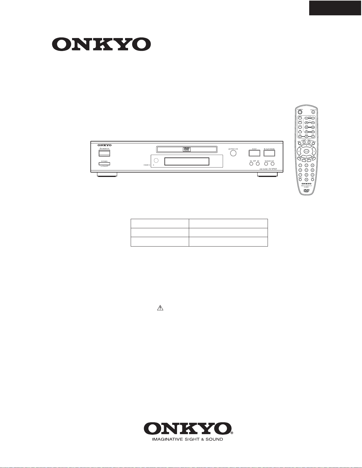
DVD PLAYER
MODEL DV-SP301
DV-SP301
Ref. No. 3761
052003
Black, Silver and Golden models
B UDD, S UDD 120V AC, 60Hz
B UUS, S UUS 230-240V AC, 50Hz
G UUK, G UUT 220-230V AC, 50/60Hz
SAFETY-RELATED COMPONENT
WARNING!!
THE MARK FOUND ON SOME COMPONENT
PARTS INDICATES THE CRITICAL FOR RISK OF
FIRE AND ELECTRIC SHOCK.
WHEN REPLACING, BE SURE TO USE PARTS OF
IDENTICAL DESIGNATION.
MAKE LEAKAGE-CURRENT OR RESISTANCE
MEASUREMENTS TO DETERMINE THAT EXPOSED
PARTS ARE ACCEPTABLY INSULATED FROM THE
SUPPLY CIRCUIT BEFORE RETURNING THE
APPLIANCE TO THE CUSTOMER.
RC-458DV
Page 2

SPECIFICATIONS
DVD Player
Power supply AC120 V, 60 Hz (North America models)
AC 110-240V, 50/60Hz (Other models)
Power consumption 16 W
Weight
External dimensions
Signal system
Regional restriction code Region 1 (North America)
(region number) Region 4 (Central and South America and Australia)
Frequency range (digital audio) 48 kHz sampling 4 Hz to 22 kHz
(DVD linear sound) 96 kHz sampling 4 Hz to 44 kHz
Signal-to-noise ratio (digital audio) More than 90 dB
Audio dynamic range (digital audio) More than 95 dB
Harmonic distortion (digital audio) Less than 0.005 %
Wow and flutter Below measurable level
Operating conditions Temperature: 5˚C to 35˚C (41˚F to 95˚F)
8.2 lbs
17-1/8" x 3-7/8" x 12-11/16" (W/H/D)
NTSC (North America models)
PAL/NTSC (Other models)
Operation status: Horizontal
DV-SP301
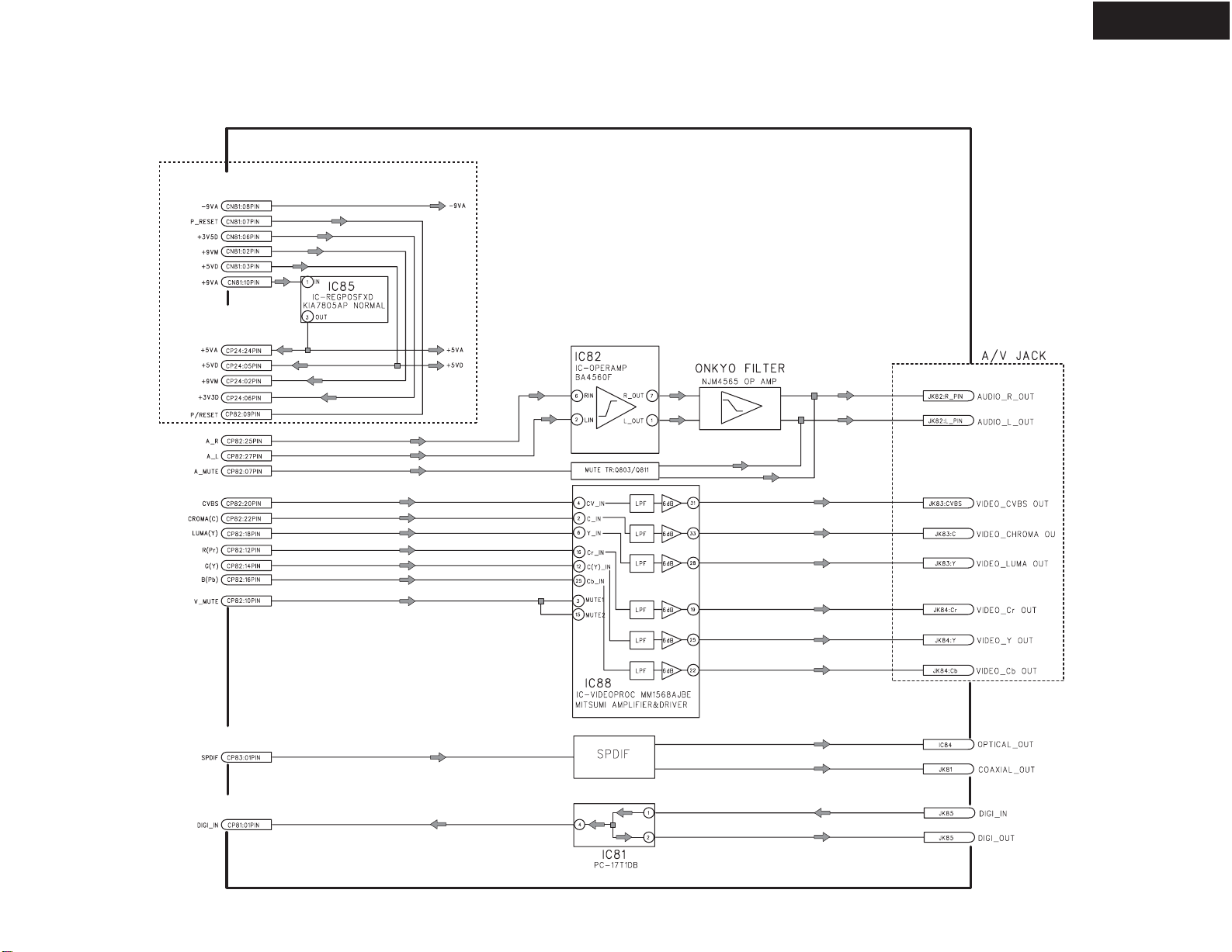
Outputs
Video output 1.0 V (p-p), 75 W, negative sync., pin jack 1
S-video output (Y) 1.0 V (p-p), 75 W, negative sync., Mini DIN 4-pin 1
(C) 0.286 V (p-p), 75 W
Component video output (Y) 1.0 V (p-p), 75 W, negative sync., pin jack 1
(PB)/(PR) 0.7 V (p-p), 75 W,
Audio output (digital output Optical) Optical connector 1
Audio output (digital output Coaxial) 0.5 V (p-p), 75 W, pin jack 1
Audio output (2-Channel Audio) 2.0 V (rms), 320 W, pin jack (L, R) 1
Specifications and features are subject to change without notice.
x
pin jack 2
x
x
x
x
x
x
Page 3
SERVICE PROCEDURE
SAFETY CHECK
(Only U.S.A. model)
After correcting the original service problem perform the
following safety check before releasing the set to the customer
Connect the insulating-resistance tester between the plug of
power supply cord and terminal GND on the back panel.
Specifications: More than 10M ohm at 500V
The lightning flash with arrowhead symbol, within an equilateral triangle, is
intended to alert the user to the presence of uninsulated "dangerous voltage"
within the product's enclosure that may be of sufficient magnitude to constitute
a risk of electric shock to persons.
The exclamation point within an equilateral triangle is intended to alert the user
to the presence of important operating and maintenance (servicing) instruction
in the literature accompanying the appliance.
LASER CAUTION
WARNING
RISK OF ELECTRIC SHOCK
DO NOT OPEN
AVIS
RISOUE DE CHOC ELECTRIQUE
NE PAS OUVRIR
DV-SP301
This unit contains a semiconductor laser system and is classified as a
CAUTION
VISIBLE AND INVISIVLE LASER RADIATION
WHEN OPEN DO NOT STARE INTO THE BEEM OR
VIEW DIRECTLY WITH OPTICAL INSTRUMENTS.
DO NOT PRESS ON THIS SURFACE
“CLASS 1 LASER PRODUCT”. So, to use this model properly, read
this Instruction Manual carefully. In case of any trouble, please contact
the store where you purchased the unit. To prevent being exposed to the
laser beam, do not try to open the enclosure.
CAUTION:
VISIBLE LASER RADIATION WHEN OPEN AND INTERLOCK
FAILED OR DEFEATED. DO NOT STARE INTO BEAM.
CAUTION:
THIS PRODUCT UTILIZES A LASER. USE OF CONTROLS OR
ADJUSTMENTS OR PERFORMANCE OF PROCEDURES OTHER
THAN THOSE SPECIFIED HEREIN MAY RESULT IN
HAZARDOUS RADIATION EXPOSURE.
REPLACING THE FUSES
CIRCUIT NO. PART NO. DESCRIPTION
F1 0215002_M Fuse, 250V 2A
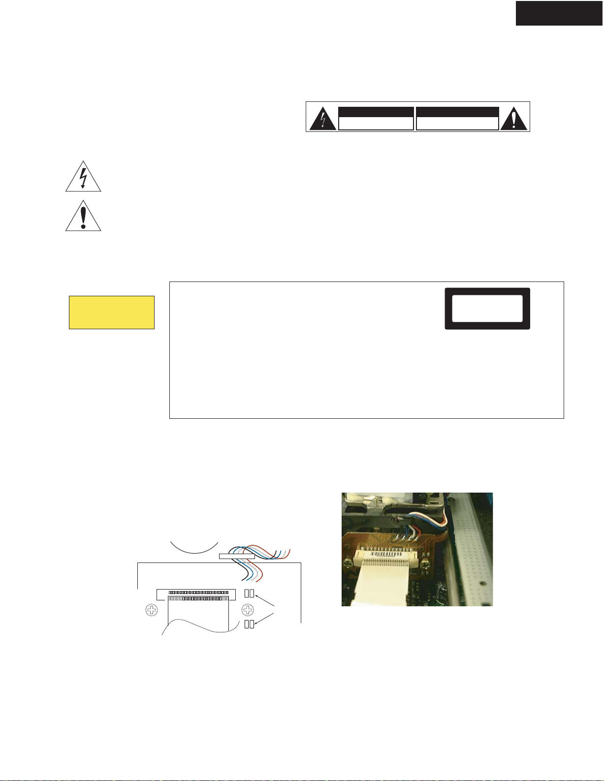
1.Remove the solder of Laser Diode shorting
1-1 Remove the bracket magnet.
1-2 Shorting the short land with solder.
1-3 Remove the FFC (CC21) and other connectors.
The label on the right is
applied on the rear
panel except for USA
and Canadian models.
1. This unit is a CLASS 1 LASER PRODUCT and employs a laser
inside the cabinet.
2. To prevent the laser from being exposed, do not remove the
cover. Refer servicing to qualified personnel.
“CLASS 1 LASER
PRODUCT
”
FFC
Short land
2. Factory setting (Initial setting)
2-1 Push the power switch "ON" (Mechanical switch)
2-2 Press the [STOP] and [STANDBY ON] keys at same time, and
it waits until the display of FL tube will be the display of "No Disc" from "Loading".
Page 4
SERVICE PROCEDURE-2
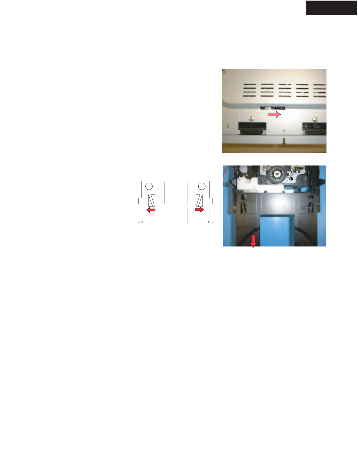
Replace the DVD mechanism
1. Remove the top cover (six screws)
2. Remove two screws of both side of front panel.
3. Remove the bracket mecha. (two screws).
4. Shift the cam slider on bottom side. (See Fig-1)
5. Remove the tray.
6. Remove FFC, connector and one screw (Mecha. GND wire).
7. A tray is drawn out extending a nail. (See Fig-2)
8. Remove two screws (3 x 6 upper side) and
two screws (3 x 8 bottom side).
DV-SP301
Bottom side
Fig-1
Page 5
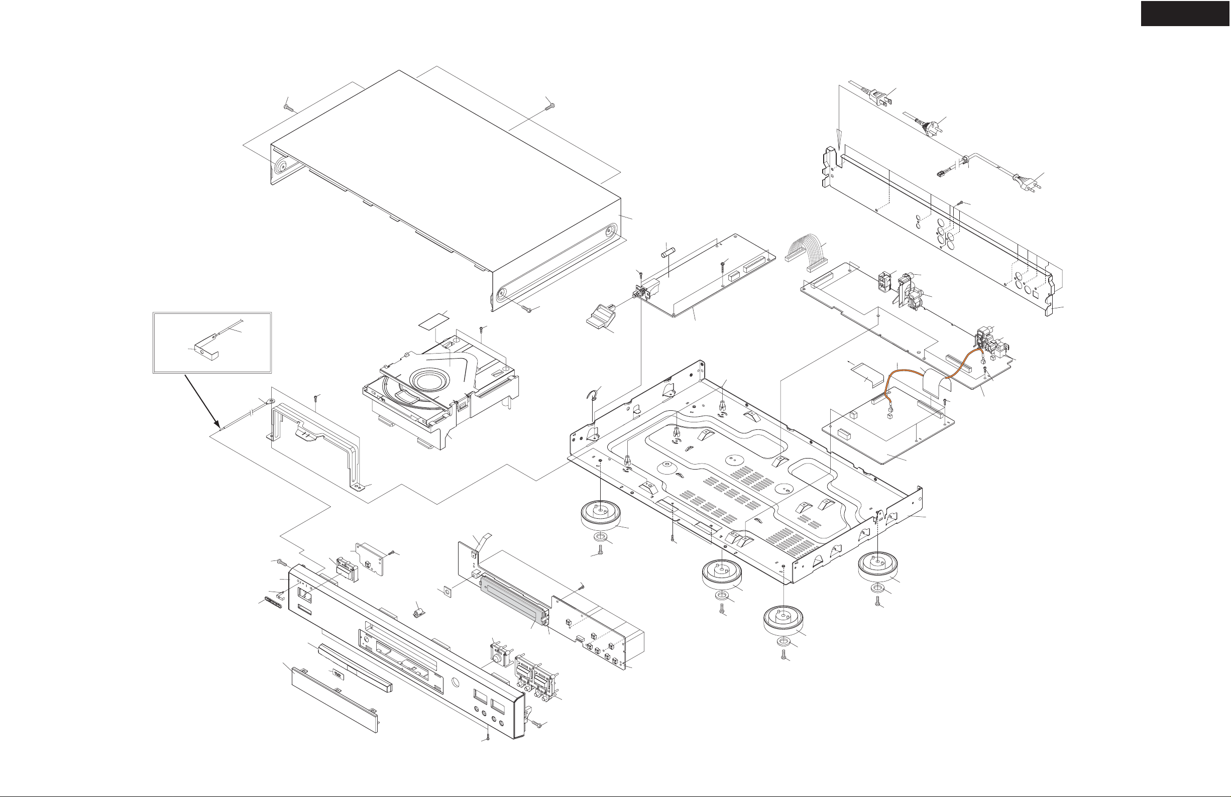
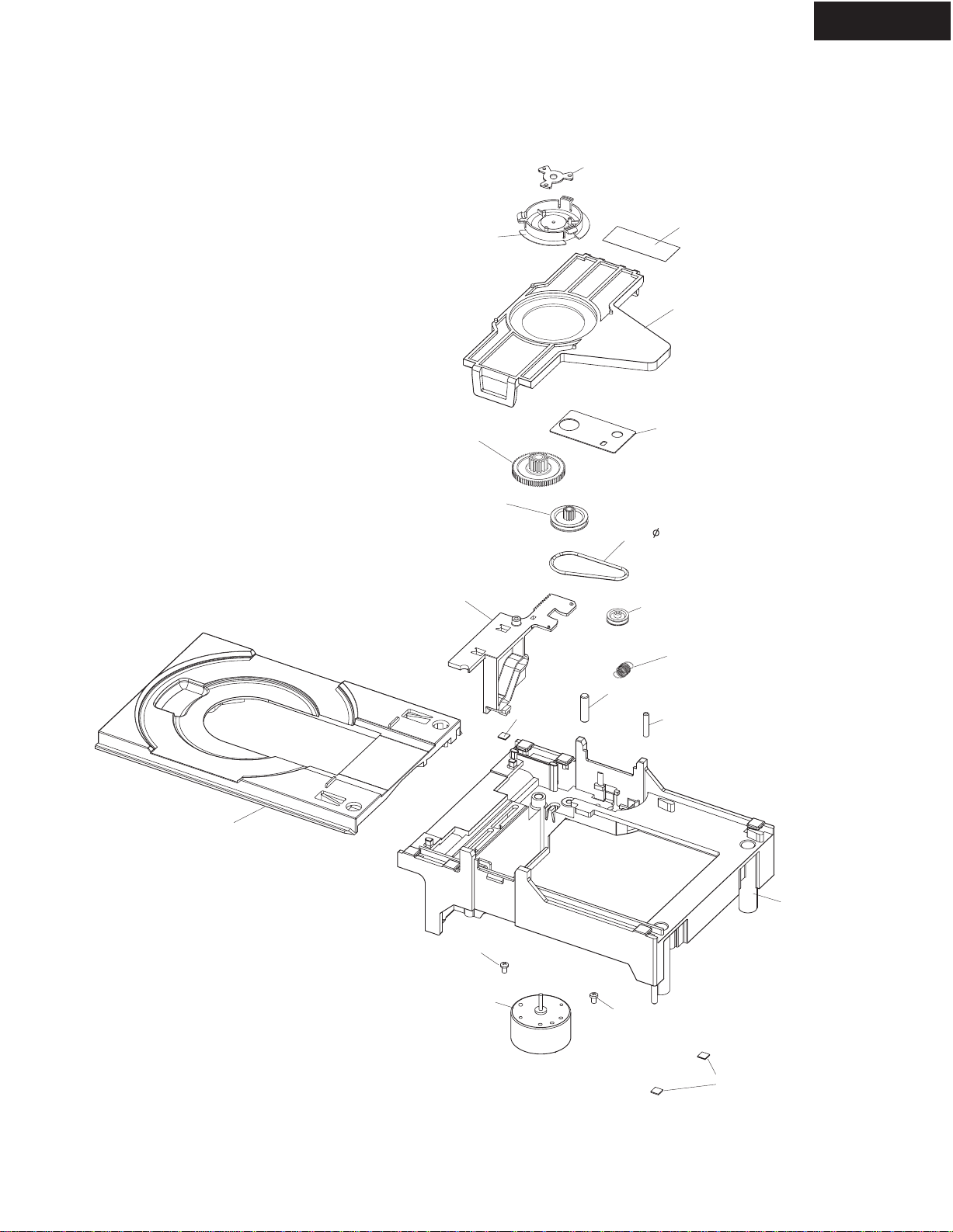
EXPLODED VIEW
DV-SP301
CHASSIS
UUD1N
S3 x 2
S3 x 2
30
UUK3P
30
UUS4P & UUT3P
29
30
S4 x 11
33
F1
CN81
S5 x 3
S2 x 2
41
N
O
I
T
A
C
36
S1 x 2
7
36
S2 x 2
S3 x 2
32
40 x 3
31
To Mecha.
37 x 3
CC21
CN25
27
CC24
26
25
S2 x 4
28
24
23
22
S2 x 5
19
34
20
35
19
17
18
16
S8 x 2
S8
17
18
S8
17
18
S8
17
18
SCREW
S1
3 x 6Y BK/BH
S2
3 x 8 ZNY/BH
S3
3 x 10 BK/BH <B>
3 x 8 Silver/BH <S> <G>
S4
3 x 10 BK/BH DOT
S5
3 x 18 W/Washer
S6
3 x 10 BK/BH <B>
3 x 8 W/Washer <S> <G>
S7
2.6 x 8 ZNY/PH
S8
3 x 10 BK/BH
S9
3 x 8 BK/FH
1
4
S9
5
6
7
8
9
S7 x 3
3
S8
S7 x 8
2
13
14
15
11
10
NOTE: <B>: Black color
12
<S>: Silver color
<G>: Golden color
S9
S6
Page 6
EXPLODED VIEW
DVD MECHANISM-1 (TVM503R6)
DV-SP301
Yoke pick
10698670
Pick load
10765150
Gear compound
10775110
Gear pulley
10775120
Cam slider
1072725A
Felt
10738740
Gear cover
10727240
Belt 28
10778340
Belt wheel
(10775090)
Gear pin 1
10778520
Label caution 2 TD
10763260
Bracket magnet 2
10763050
Spring slider
10727210
Gear pin 2
10783720
Tray
10793320
Screw 2.6 x 4mm
20349530
Motor DC MSN5E358A
(20581790)
Screw 2.6 x 4mm
20349530
Bracket support
1072717A
Drive moment 12N.cm (+/-2N.cm)
Apply screw lock (0.022g)
Felt
10738740
Page 7
EXPLODED VIEW
DVD MECHANISM-2 (TVM503R6)
Bracket DVD
10727260
TVM503 R-6
10724940
2 x Screw-ST 3mm x 10mm
205835800
Driver moment 25N.cm (+/- 2N.cm)
DV-SP301
4 x Screw shoulder 2 x 14.7mm
Driver moment 28N.cm (+/-3N.cm)
Belt wheel mounting
Motor assy part no. 10840810
Belt wheel (10775090)
Motor (20581790)
Felt position 10738740
10742170
4 x Cushion 8
10741230
Cushion mounting
3.1 +/- 0.1
On bracket support:
In the groove of Bracket DVD rotation axle
going half outside the groove
Screw 10742170
Bracket DVD 10727260
Cushion 8 10741230
Main plate
On Cam slider
Page 8
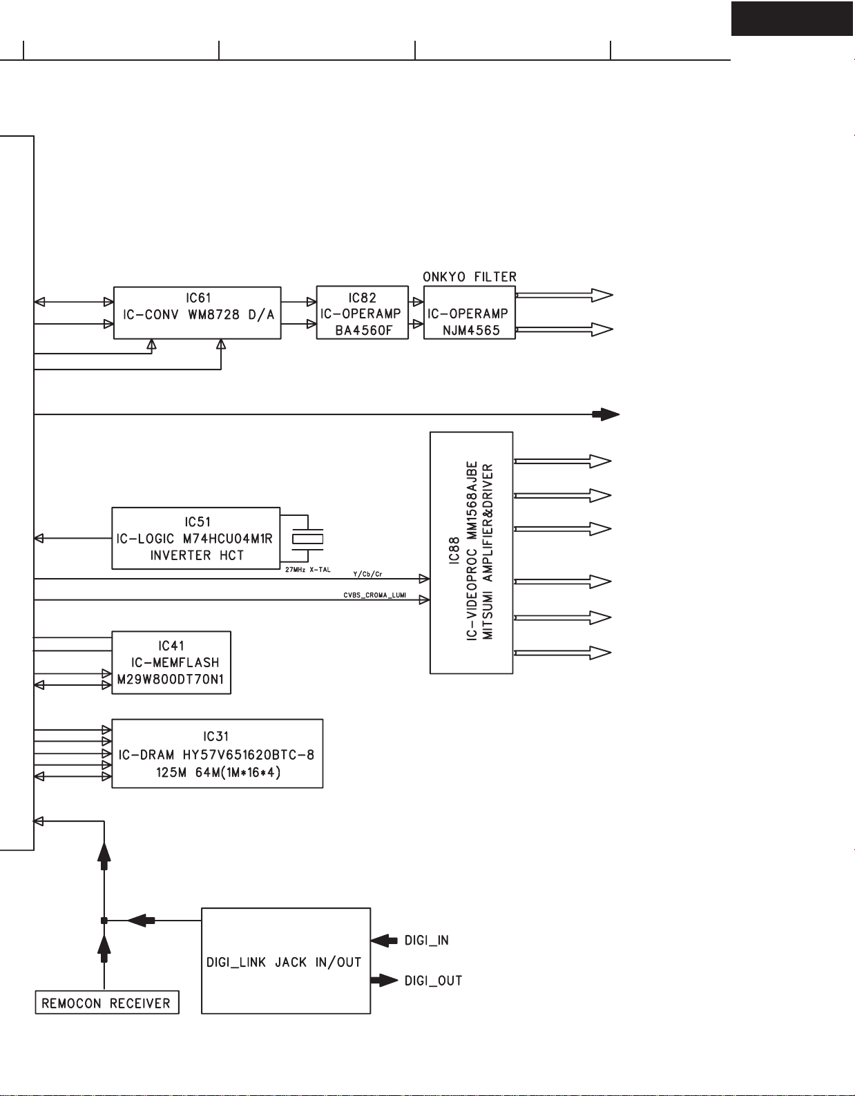
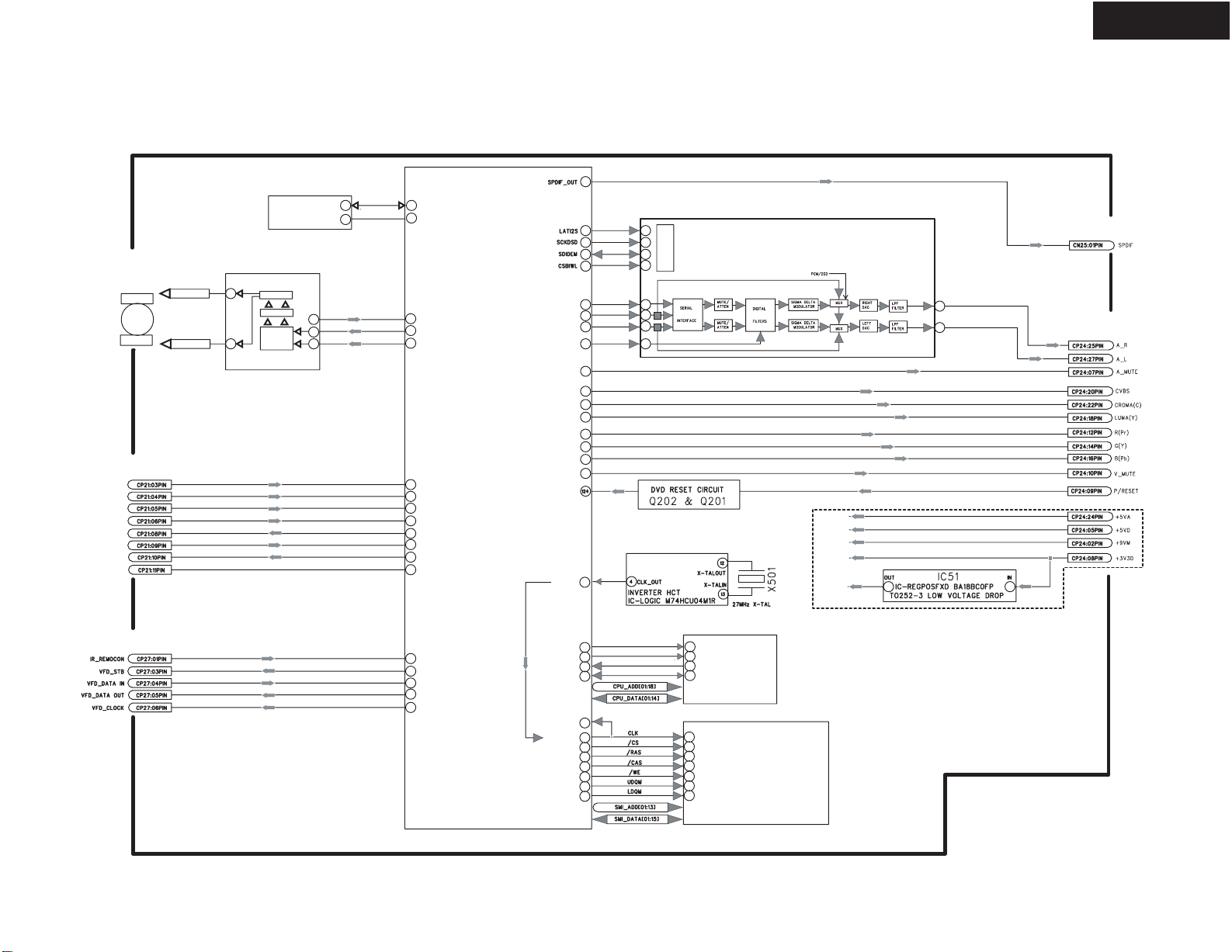
DV-SP301
SDIDEM
MCLK
SERIAL INTERFACE
(BCKIN/LRCIN/DIN)
MODE/LAT12S/SCKDSD/CSBIWL
W/E/G/RP
BYTE/RB
CPU_ADD (01:18)
CPU_DATA (01:14)
VOUTL
VOUTR
AUDIO_OUT_L
AUDIO_OUT_R
SPDIF_OUT
Y
Cb
Cr
S
C
Y
(Y) LUMINANCE_OUT
(Cb) BLUE_OUT
(Cr) RED_OUT
COMPOSITE_OUT
CHROMINANCE_OUT
LUMINANCE_OUT
CLK
UDQM/LDQM/
CA/CAS/RAS/WE
SMI_ADD (01:13)
SMI_DATA (01:15)
Page 9
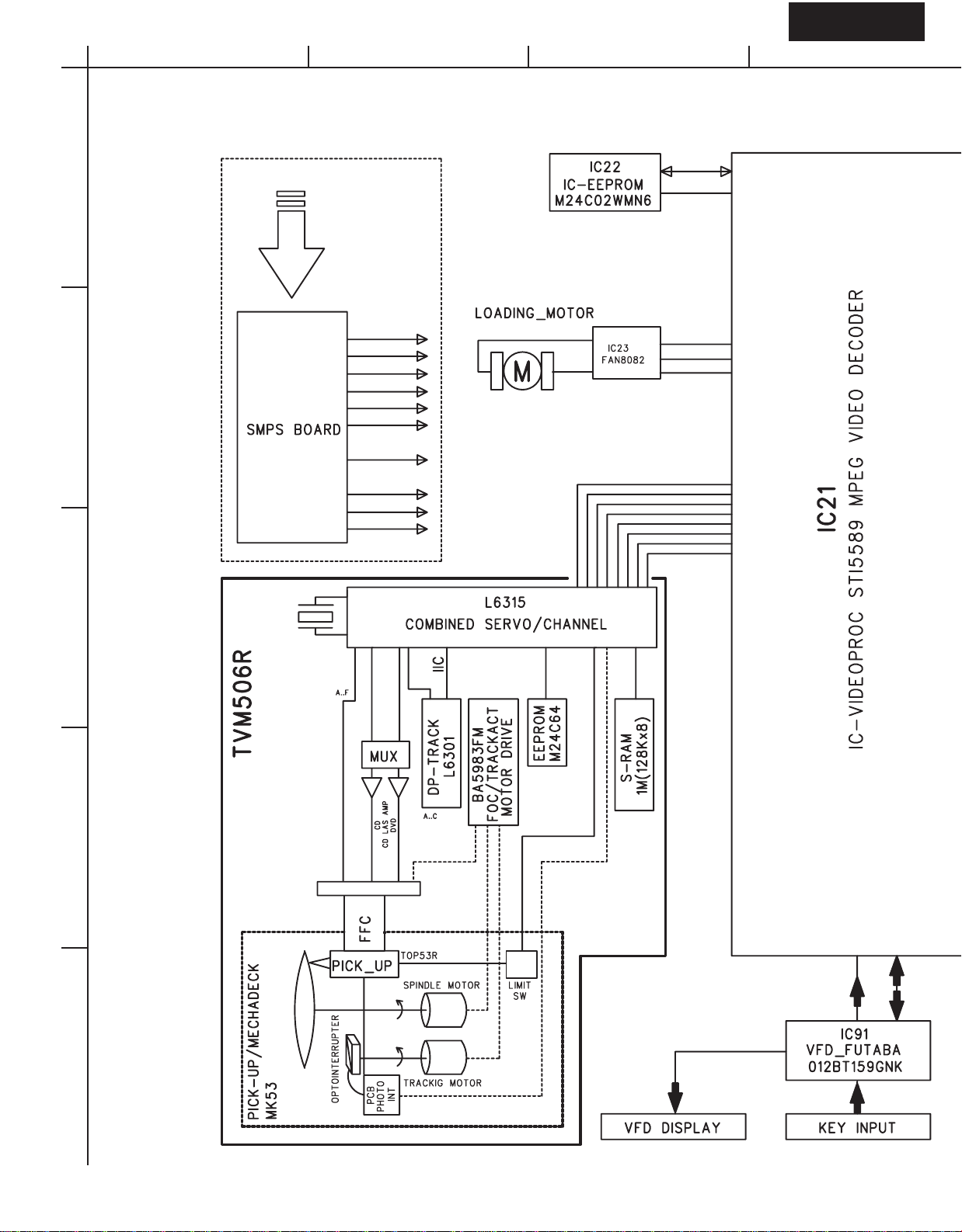
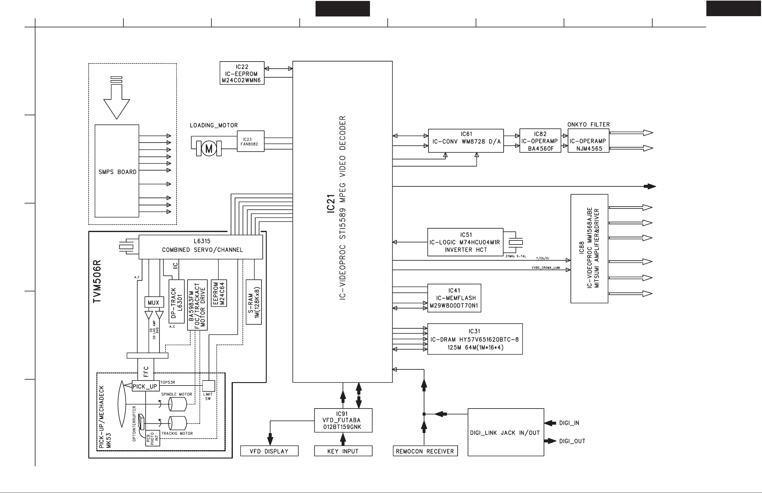
DV-SP301
A
BLOCK DIAGRAM
OVERALL
1
2
+FL5V
-FL27V
-FL5V
+5V6S
+9VA
-9VA
+3V5D
+5VD
+9V_MOTOR
A_D_M_GND
BCDEFGH
IIC DATA
IIC CLK
LO_MO-
LO_MO+
OPEN/CLOSE
SLIDE_IN
SLIDE_OUT
IIC DATA
IIC CLK
SXX_INT
DVD_RESET
BCLK
DATA
PACKCLK
S_START
3
4
VFD_CONTROL
5
Page 10
DV-SP301
DV-SP301
A
BLOCK DIAGRAM
OVERALL
1
2
3
+FL5V
-FL27V
-FL5V
+5V6S
+9VA
-9VA
+3V5D
+5VD
+9V_MOTOR
A_D_M_GND
BCDEFGH
IIC DATA
IIC CLK
LO_MO-
LO_MO+
IIC DATA
IIC CLK
SXX_INT
DVD_RESET
BCLK
DATA
PACKCLK
S_START
OPEN/CLOSE
SLIDE_IN
SLIDE_OUT
SDIDEM
MCLK
SERIAL INTERFACE
(BCKIN/LRCIN/DIN)
MODE/LAT12S/SCKDSD/CSBIWL
VOUTL
VOUTR
Y
Cb
Cr
AUDIO_OUT_L
AUDIO_OUT_R
SPDIF_OUT
(Y) LUMINANCE_OUT
(Cb) BLUE_OUT
(Cr) RED_OUT
S
C
W/E/G/RP
BYTE/RB
CPU_ADD (01:18)
CPU_DATA (01:14)
CLK
4
VFD_CONTROL
UDQM/LDQM/
CA/CAS/RAS/WE
SMI_ADD (01:13)
SMI_DATA (01:15)
Y
COMPOSITE_OUT
CHROMINANCE_OUT
LUMINANCE_OUT
5
Page 11
DV-SP301
BLOCK DIAGRAM
To Power supply
To DVD
Main circuit
POWER SUPPLY
OUTPUT TERMINAL CIRCUIT
To Main PCB
To Display PCB
Page 12
BLOCK DIAGRAM
DVD MAIN CIRCUIT
LOADING_MOTOR
CP28:01PIN
M
CP28:02PIN
To PICK_UP
2
8
IC22
IC-EEPROM
M24C02WMN6
IC23
DRIVE_OUT
PRE_DRIVE
LOGIC_SW
FAN8082
MOTOR_DRIVE
DV-SP301
57
IIC DATA
5
SDA
IIC CLK
6
SCL
6
5
6
IIC_DATA
194
IIC_CLK
195
SLIDE_SEN(O/C)
192
193
SLIDE_IN
196
SLOIDE_OUT
19
SECTOR_START
18
EXT_DATA
16
EXT_BCLK
17
BIT_CLK
13
DVD_RESET
127
DXX_INTERRUPT
195
IIC_CLK
194
IIC_DATA
IC21
PCM_BCK
DAC_LRCLK
DAC_PCM_DATA
DAC_PCM_CLK
AUDIO_MUTE
CV_OUT
C_OUT
Y_OUT
Cr_OUT
G(Y)_OUT
Cb_OUT
VIDEO_MUTE
RESET
PIX_CLK
44
41
42
45
51
56
52
55
208
34
33
32
27
26
25
2
20
19
18
CONTROL
INTERFACE
15
3
1
2
4
IC61
IC-CONV WN8728 D/A
VOUT R
VOUT L
8
11
To OUT
To OUT
+5VA
+5VD
+9VM
IC51
120
+3V3D
+1V8D
31
To DISPLAY PCB
10
188
191
190
189
IR_REMOCON
VFD_STB
DATA_IN
DATA_OUT
VFD_CLOCK
/W
11
128
CPU_BE
132
CPU_CE
117
CPU_OE
124
F_RESET
IC-VIDEO PROC STI5589 MPEG VIDEO DECODER
SMI_CLKIN
SMI_CLKOUT
UDQM
LDQM
82
95
74
/CS
76
/RAS
77
/CAS
78
/WE
80
79
/E
/G
/RP
26
28
12
38
SMI_CLKOUT
19
/CS
18
/RAS
17
/CAS
16
/WE
39
UDQM
15
LDQM
/W
/E
/G
/RP
IC-MEMFLASH
M29W800DT70N1
IC41
IC31
IC-DRAM HY57V561620BTC-8
125M 64M (1M*16*4)
POWER SUPPLY
Page 13

BLOCK DIAGRAM
DISPLAY CIRCUIT
DV-SP301
FL91
VFD_012BT159GNK
From Power supply unit
RM91
38KHz
IC91
IC-DISPLAY uPD16311GC-AB6 HIGH VOLTAGE DRIVER
To Output Terminal
To Main circuit
Page 14
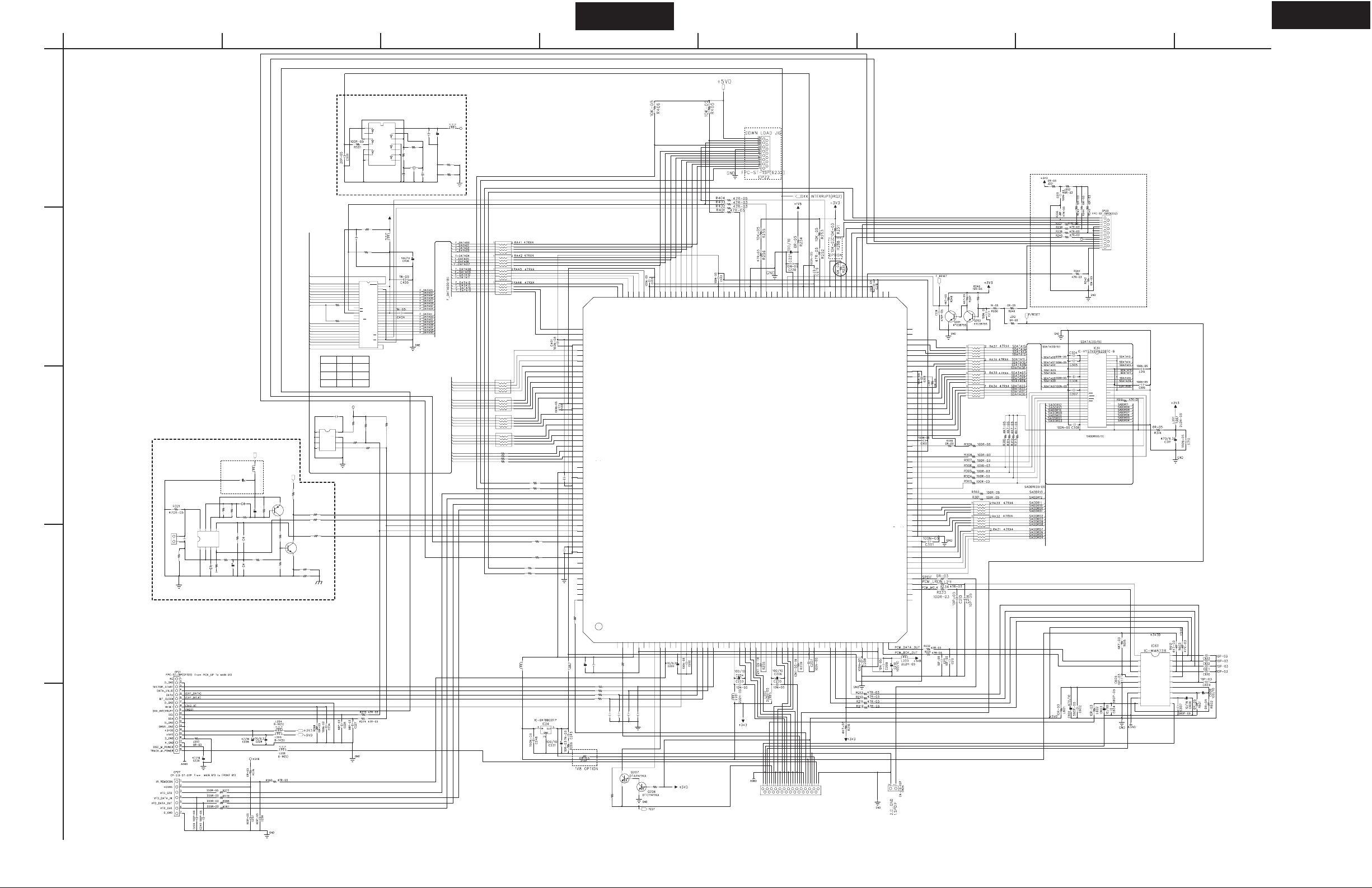
DV-SP301
DV-SP301
A
SCHEMATIC DIAGRA
MAIN CIRCUIT PC BOARD
1
2
3
1
100N-05
2
CP28
CP-2.5-ST-02P(XH)
From Main PCB to Pick up
R322
470R-05
4
+8V_MOTOR_LOADING_VCC
R329
876
5
C251
VO2
VIN2
PVCC
SVCC
IC23
GND
VO1
VCTL
VIN1
IC-FAN8082
123
4
R323
5K6-05
R327
10K-05
D201
UZ5V6
Motor Driver
BCDEFGH
IC51
IC-M74HCU04M1R
INVERTER
14
1
A0
VCC
13
2
O0
A3
12
3
A1
O3
11
4
O1
A4
R503
10
5
A2
O4
1M-05
9
6
O2
A5
R502
8
7
F_ADDR17
F_ADDR16
F_ADDR15
F_ADDR14
F_ADDR13
F_ADDR12
F_ADDR11
F_ADDR10
F_ADDR09
F_ADDR20
F_ADDR19
F_ADDR18
F_ADDR08
F_ADDR07
F_ADDR06
F_ADDR05
F_ADDR04
F_ADDR03
F_ADDR02
F_ADDR01
ATM EL
GND
R416
1K-05
C407
100N-05
R413 47K-05
IC41
IC-M29W800AT90N1
1
A16
A15
2
BYTE
A14
3
VSS
A13
4
DQ15
A12
5
DQ7
A11
6
DQ14
A10
7
DQ6
A9
8
DQ13
A8
9
DQ5
NC
10
DQ12
NC
R411
11
DQ4
WE
0R-03
12
VCC
RP
13
DQ11
NC
R412
14
DQ3
NC
0R-03
15
DQ10
RY/BY
16
DQ2
A18
17
DQ9
A17
18
DQ1
A7
19
DQ8
A6
20
DQ0
A5
21
QE
A4
22
VSS
A3
23
CE
A2
24
A0
A1
R412
R411
ST
NC
0 Ohm
16M
0 Ohm
NC
16M
ST
NC
NC
8M
56R-05
O5
X501
27M0
C502
22P-05
+3.3VM
R415
B-1K(S)
48
47
46
45
44
43
42
41
40
39
38
37
36
35
34
33
32
31
30
29
28
27
26
25
+5V6S
100N-03
C225
IC22
IC-M24C02WMN6
1
E0
2
E1
3
E2
4
VSS
R333
47K-03
R336 0R-03
R337 0R-05
R338 0R-05
Q203
KTC3875S
J511 0R-03
J512 0R-03
CHGND
Sub EPROM
+5V_DIGI_VCC
L207
22UH-05
C254
100/16
1N414B
Q204
D204
R330
22R-05
R328
5K6-05
R331
10K-05
1N4148
R332
C253
10/16
1K8-05
KTA1504(S)
R326
RB441Q
10K-05
10K-05
R324
R325
68K-03
D202
D203
22R-05
1/50
C252
R266
10R-03
8
VDD
7
WC
R267
6
SCL
47R-05
5
SDA
GND
47R-05
27K-03
R268
R270
2K7-03
R269
100N-05
C504
L501
B-1K(S)
D3V3
C505
470/6.3
0R-03
R511
0R-03
C503
R512
22P-05
GND
F_ADDR [01:21]
F_ADDR01
F_ADDR02
F_ADDR03
F_ADDR04
F_ADDR05
F_ADDR06
F_ADDR07
F_ADDR08
F_ADDR09
F_ADDR10
F_ADDR11
F_ADDR12
F_ADDR13
F_ADDR14
F_ADDR15
F_ADDR16
F_ADDR17
F_ADDR18
F_ADDR19
F_ADDR20
RA45 47Rx4
12
RA46 47Rx4
12
RA47 47Rx4
12
RA48 47Rx4
12
47R-03
R407
47R-03
R408
47R-03
R409
47R-03
R410
TRIGIN
TRIGOUT
L209
R262 47R-03
R263 47R-03
R289 47R-03
R290 47R-03
R264 75R-03
R265 75R-03
2U2H-05
156
155
154
CPU_DATA(13)
CPU_DATA(12)
(BLANK)
C201
C235
10P-05
CPU_DATA(11)
PIO2(5) RGB_SEL
PIO2(6) VIDEO_MUTE
PIO2(7) 16:9_INDICATOR
123456789
R221
100R-03
C244
10P-05
10P-05
157
CPU_DATA(14)
158
CPU_DATA(15)
159
VDD3_3
160
VSS
161
CPU_ADR(1)
162
CPU_ADR(2)
163
CPU_ADR(3)
164
CUP_ADR(4)
165
CUP_ADR(5)
166
CPU_ADR(6)
167
CUP_ADR(7)
168
CUP_ADR(8)
169
CPU_ADR(9)
170
CPU_ADR(10)
171
VDD2_5
172
VSS
173
CUP_ADR(11)
174
CPU_ADR(12)
175
CPU_ADR(13)
176
CPU_ADR(14)
177
CPU_ADR(15)
178
CPU_ADR(16)
179
CPU_ADR(17)
180
CPU_ADR(18)
181
CPU_ADR(19)
182
CPU_ADR(20)
183
CPU_ADR(21)
184
VDD_3
185
VSS
C403
186
100N-05
PIO0(0) T_SROBE
187
PIO0(1) MOD_SW
188
PIO0(2) VFD_STB
189
PIO0(3) VFD_CLK
190
PIO0(4) VFD_DATA_OUT
191
PIO0(5) VFD_DATA_IN
192
PIO0(6) SLIDER_SENSOR_OPEN/CLOSE (DRAWER_POSITION_P
193
PIO0(7) SLIDER_IN(DRAWER_CCW_CTRL)
194
PIO1(0) SDA
195
PIO0(1) SCL
196
PIO1(2) SLIDER_OUT (DRAWER_CW_CTRL)
197
PIO1(3) TXD (JIG)
198
VDD_5
199
VSS
C224
100N-05
200
PIO1(4) RXD (JIG)
201
PIO1(5) FRONT_TXD1
202
TRIGGER_IN
203
TRIGGRER_OUT
GND
204
PIO2(0) H/P_IND
205
PIO2(1) FRONT_RXD
206
PIO2(2) MIC_DET
207
PIO2(3) MIC_MUTE
208
PIO2(4) AUDIO_MUTE
R223
47R-03
C232
L208
100/10
100N-05
2U2H-05
100R-05 R201
100R-05 R202
100R-05 R203
100R-05 R204
153
152
151
150
149
148
147
146
145
144
143
142
141
140
139
138
137
136
135
134
133
132
131
130
129
128
127
126
125
124
123
122
121
120
119
VSS
VDD2_5
CPU_DATA(9)
CPU_DATA(8)
CPU_DATA(7)
CPU_DATA(6)
CPU_DATA(5)
CPU_DATA(4)
CPU_DATA(10)
CPU_DATA(3)
VSS
VDD3_3
CPU_RW
CPU_WAIT
CPU_BE(1)
CPU_CE(1)
CPU_CE(2)
CPU_CE(3)
CPU_BE(0)
CPU_CE(0)
CPU_CAS1
CPU_CAS0
CPU_RAS1
CPU_DATA(2)
CPU_DATA(1)
CPU_DATA(0)
IRQ(0)
IRQ(1)
IRQ(2)
RESET
VSS_PLL
VDD_PLL
VSS
VDD2_5
PIX_CLK
IC21
STI5589
VDD3_3
VSS
PIO3(0) SCART_H (TV/AUX)
PIO3(1)
PIO3(2)
PIO3(3)
PIO3(4) IR (REMOCON)
PIO3(5)
PIO3(6)
PIO3(7) DVD_RESET
VDD2_5
VSS
B_DATA
B_BCLK
B_FLAG
B_SYNC
B_WCLK
B_V4
NRSS_OUT
VDD_RGB
VSS_RGB
B_OUT
G_OUT
R_OUT
V_REF_RG
I_REF_RG
VDD_YCC
VSS_YCC
Y_OUT
C_OUT
CV_OUT
V_REF_YC
I_REF_YC
VDD2_5
10111213141516171819202122232425262728293031323334353637383940414243444546474849505152
C242
C243
10P-05
GND
VSS
118
117
116
115
114
PWM0
PWM1
PWM2
CPU_OE
CPU_PROCLK
PIO4(0) H/P_MUTE
PIO4(1)
PIO4(2) DAC_SCKDSO
PIO4(3) DAC_SDIDEM
PIO4(4) DAC_MUTEB
113
TCK
PIO4(5) DAC_LAT12S
112
111
TDI
TDO
PIO4(6) DAC_CSBIWL
PIO4(7) DAC_ZERO
110
109
108
107
VSS
TMS
TRST
VDD3_3
SMI_DATA(15)
SMI_DATA(14)
SMI_DATA(13)
SMI_DATA(12)
SMI_DATA(11)
SMI_DATA(10)
SMI_CLKOUT
(LRCIN) DAC_LRCLK
(MCLK) DAC_PCMCLK
DAC_PCMOUT2
DAC_PCMOUT1
VDD3_3
VDD_PCM
VSS_PCM
VSS
106
105
ADC_DATA
ADC_PCMCLK
ADC_LRCLK
ADC_SCLK
VDD2_5
SMI_DATA(9)
SMI_DATA(8)
SMI_DATA(7)
SMI_DATA(6)
SMI_DATA(5)
SMI_DATA(4)
SMI_DATA(3)
SMI_DATA(2)
SMI_DATA(1)
SMI_DATA(0)
SMI_CLKIN
VDD3_3
SMI_DQMU
SMI_DQML
SMI_WE
SMI_CAS
SMI_RAS
SMI_CS(1)
SMI_CS(0)
SMI_ADE(13)
SMI_ADR(12)
SMI_ADR(11)
SMI_ADR(10)
SMI_ADR(0)
SMI_ADR(1)
SMI_ADR(2)
SMI_ADR(3)
VDD2_5
SMI_ADR(9)
SMI_ADR(8)
SMI_ADR(7)
SMI_ADR(6)
SMI_ADR(5)
SMI_ADR(4)
SPDIF_OUT
DAC_SCLK (BCK)
DAC_PCMOUT0 (DATA)
104
103
102
101
100
99
98
97
96
VSS
95
94
93
92
91
90
89
88
87
86
85
84
83
VSS
82
81
80
79
78
77
76
75
74
73
72
71
70
69
68
67
66
65
VSS
64
63
62
61
60
59
58
57
56
55
54
53
JTAG TEST CONNECTION
1
2
3
4
5
6
7
8
9
10
11
12
13
14
15
1
VCC
VSS
54
2
DQ0
DQ15
53
3
VCCQ
VSSQ
52
4
DQ1
DQ14
51
5
DQ2
DQ13
50
6
VSSQ
VCCQ
49
7
DQ3
DQ12
48
8
DQ4
DQ11
47
9
VCCQ
VSSQ
46
10
DQ5
DQ10
45
11
DQ6
DQ9
44
12
VSSQ
VCCQ
43
13
DQ7
DQ8
42
14
VCC
VSS
41
15
LDQM
NC
40
16
WE
UDQM
39
17
CAS
CLK
38
18
RAS
CKE
37
19
CS
NC
36
20
BA0
A11
35
21
BA1
A9
34
22
A10
A8
33
23
A0
A7
32
24
A1
A6
31
25
A2
A5
30
26
A3
A4
29
27
VCC
VSS
28
1.
TRIGOUT
2.
TRIGIN
3.
GND (option)
4.
TMS
5.
GND
6.
TCK
7.
GND
8.
TDI
9.
GND
10.
TDO
11.
+5VD
12.
TXD (JIG)
13.
RXD (JIG)
14.
JTAG_RST/
15.
TRST
LRCIN
DIN
BCKIN
MCLK
ZERO
DGND
DVDD
VOUTR
AGND
AVDD
LAT12S
SCKDSD
SDIDEM
MUTEB
CSBIWL
VREFP
VREFN
VOUTL
20
19
18
17
16
MODE
15
14
13
12
VMID
11
1
2
3
4
5
6
7
8
9
10
5
27.
26.
25.
24.
23.
22.
21.
20.
19.
18.
17.
16.
15.
14.
13.
12.
11.
10.9.8.7.6.5.4.3.2.
LUMA(Y)
A_GND
18.
17.
1.
CP24
FPC-ST-27P (GF120)
B(Pb)
A_GND
G(Y)
A_GND
R(Pr)
A_GND
V_MUTE
P/RESET
A_GND
A_MUTE
3V3D
+5VD
D_GND
+1V8VM
+9VM
M_GND
9.8.7.6.5.4.3.2.1.
16.
15.
14.
13.
12.
11.
10.
R3 100K
1k
R1
A_L
A_GND
A_R
+5VARICROMA(C)
A_GND
CVBS
A_GND
27.
26.
25.
24.
23.
22.
21.
20.
19.
To Output terminal PC board
Page 15
DV-SP301
JTAG TEST CONNECTION
1
1.
TRIGOUT
2
2.
TRIGIN
3
3.
GND (option)
4
4.
TMS
5
6
5.
GND
7
6.
TCK
8
7.
GND
9
8.
TDI
10
11
9.
GND
12
10.
TDO
13
11.
+5VD
14
12.
TXD (JIG)
15
13.
RXD (JIG)
14.
JTAG_RST/
15.
TRST
144
143
142
141
140
139
138
137
136
135
134
133
132
131
130
129
128
127
126
125
124
123
122
121
120
119
118
117
116
115
114
113
112
111
110
109
108
107
106
TDO
TMS
TRST
(LRCIN) DAC_LRCLK
(MCLK) DAC_PCMCLK
VSS
VDD3_3
SMI_DATA(15)
SMI_DATA(14)
SMI_DATA(13)
SMI_DATA(12)
SMI_DATA(11)
SMI_DATA(10)
SMI_CLKOUT
DAC_PCMOUT2
DAC_PCMOUT1
105
ADC_DATA
ADC_PCMCLK
ADC_LRCLK
ADC_SCLK
VSS
VDD2_5
SMI_DATA(9)
SMI_DATA(8)
SMI_DATA(7)
SMI_DATA(6)
SMI_DATA(5)
SMI_DATA(4)
SMI_DATA(3)
SMI_DATA(2)
SMI_DATA(1)
SMI_DATA(0)
VSS
SMI_CLKIN
VDD3_3
SMI_DQMU
SMI_DQML
SMI_WE
SMI_CAS
SMI_RAS
SMI_CS(1)
SMI_CS(0)
SMI_ADE(13)
SMI_ADR(12)
SMI_ADR(11)
SMI_ADR(10)
SMI_ADR(0)
SMI_ADR(1)
SMI_ADR(2)
SMI_ADR(3)
VSS
VDD2_5
SMI_ADR(9)
SMI_ADR(8)
SMI_ADR(7)
SMI_ADR(6)
SMI_ADR(5)
SMI_ADR(4)
SPDIF_OUT
104
103
102
101
100
99
98
97
96
95
94
93
92
91
90
89
88
87
86
85
84
83
82
81
80
79
78
77
76
75
74
73
72
71
70
69
68
67
66
65
64
63
62
61
60
59
58
57
56
55
54
53
1
VCC
VSS
54
2
DQ0
DQ15
53
3
VCCQ
VSSQ
52
4
DQ1
DQ14
51
5
DQ2
DQ13
50
6
VSSQ
VCCQ
49
7
DQ3
DQ12
48
8
DQ4
DQ11
47
9
VCCQ
VSSQ
46
10
DQ5
DQ10
45
11
DQ6
DQ9
44
12
VSSQ
VCCQ
43
13
DQ7
DQ8
42
14
VCC
VSS
41
15
LDQM
NC
40
16
WE
UDQM
39
17
CAS
CLK
38
18
RAS
CKE
37
19
CS
NC
36
20
BA0
A11
35
21
BA1
A9
34
22
A10
A8
33
23
A0
A7
32
24
A1
A6
31
25
A2
A5
30
26
A3
A4
29
27
VCC
VSS
28
VSS
VDD3_3
CPU_RW
CPU_WAIT
CPU_BE(1)
CPU_CE(1)
CPU_CE(2)
CPU_CE(3)
CPU_BE(0)
CPU_CE(0)
CPU_CAS1
CPU_CAS0
CPU_RAS1
CPU_DATA(3)
CPU_DATA(2)
CPU_DATA(1)
CPU_DATA(0)
IRQ(0)
IRQ(1)
IRQ(2)
RESET
VSS_PLL
VDD_PLL
VSS
PIX_CLK
VDD2_5
CPU_PROCLK
CPU_OE
PWM0
PWM1
PWM2
TCK
TDI
IC21
STI5589
PIO3(7) DVD_RESET
VDD2_5
VSS
B_DATA
B_BCLK
B_FLAG
B_SYNC
B_WCLK
B_V4
NRSS_OUT
VDD_RGB
VSS_RGB
B_OUT
G_OUT
R_OUT
V_REF_RG
I_REF_RG
VDD_YCC
VSS_YCC
Y_OUT
C_OUT
CV_OUT
V_REF_YC
I_REF_YC
VDD2_5
VSS
PIO4(0) H/P_MUTE
PIO4(1)
PIO4(2) DAC_SCKDSO
PIO4(3) DAC_SDIDEM
PIO4(4) DAC_MUTEB
PIO4(5) DAC_LAT12S
PIO4(6) DAC_CSBIWL
PIO4(7) DAC_ZERO
VDD3_3
VDD_PCM
VSS_PCM
131415161718192021222324252627282930313233343536373839404142434445464748495051
27.
26.
25.
24.
23.
22.
21.
20.
19.
18.
17.
16.
15.
14.
13.
12.
11.
10.9.8.7.6.5.4.3.2.
1.
CP24
VSS
FPC-ST-27P (GF120)
A_L
A_GND
A_R
+5VARICROMA(C)
A_GND
CVBS
A_GND
LUMA(Y)
A_GND
B(Pb)
A_GND
G(Y)
A_GND
R(Pr)
A_GND
V_MUTE
P/RESET
A_GND
A_MUTE
3V3D
+5VD
D_GND
+1V8VM
+9VM
M_GND
27.
26.
25.
24.
23.
22.
21.
To Output terminal PC board
20.
19.
18.
9.8.7.6.5.4.3.2.1.
17.
16.
15.
14.
13.
12.
11.
10.
DAC_SCLK (BCK)
DAC_PCMOUT0 (DATA)
52
LRCIN
DIN
BCKIN
MCLK
ZERO
DGND
DVDD
VOUTR
AGND
AVDD
LAT12S
SCKDSD
SDIDEM
MUTEB
MODE
CSBIWL
VREFP
VREFN
VOUTL
20
19
18
17
16
15
14
13
12
VMID
11
1
2
3
4
5
6
7
8
9
10
Page 16
DV-SP301
A
SCHEMATIC DIAGRA
MAIN CIRCUIT PC BOARD
1
2
3
1
100N-05
2
CP28
CP-2.5-ST-02P(XH)
From Main PCB to Pick up
R322
470R-05
4
+8V_MOTOR_LOADING_VCC
R329
876
5
C251
VO2
VIN2
PVCC
SVCC
IC23
GND
VO1
VCTL
VIN1
IC-FAN8082
123
4
R323
5K6-05
R327
10K-05
D201
UZ5V6
Motor Driver
BCDEFGH
IC51
IC-M74HCU04M1R
INVERTER
14
1
A0
VCC
13
2
O0
A3
12
3
A1
O3
11
4
O1
A4
R503
10
5
A2
O4
1M-05
9
6
O2
A5
R502
8
7
F_ADDR17
F_ADDR16
F_ADDR15
F_ADDR14
F_ADDR13
F_ADDR12
F_ADDR11
F_ADDR10
F_ADDR09
F_ADDR20
F_ADDR19
F_ADDR18
F_ADDR08
F_ADDR07
F_ADDR06
F_ADDR05
F_ADDR04
F_ADDR03
F_ADDR02
F_ADDR01
ATM EL
GND
R416
1K-05
C407
100N-05
R413 47K-05
IC41
IC-M29W800AT90N1
1
A16
A15
2
BYTE
A14
3
VSS
A13
4
DQ15
A12
5
DQ7
A11
6
DQ14
A10
7
DQ6
A9
8
DQ13
A8
9
DQ5
NC
10
DQ12
NC
R411
11
DQ4
WE
0R-03
12
VCC
RP
13
DQ11
NC
R412
14
DQ3
NC
0R-03
15
DQ10
RY/BY
16
DQ2
A18
17
DQ9
A17
18
DQ1
A7
19
DQ8
A6
20
DQ0
A5
21
QE
A4
22
VSS
A3
23
CE
A2
24
A0
A1
R412
R411
ST
NC
0 Ohm
16M
0 Ohm
NC
16M
ST
NC
NC
8M
56R-05
O5
X501
27M0
C502
22P-05
+3.3VM
R415
B-1K(S)
48
47
46
45
44
43
42
41
40
39
38
37
36
35
34
33
32
31
30
29
28
27
26
25
+5V6S
100N-03
C225
IC22
IC-M24C02WMN6
1
E0
2
E1
3
E2
4
VSS
R333
47K-03
R336 0R-03
R337 0R-05
R338 0R-05
Q203
KTC3875S
J511 0R-03
J512 0R-03
CHGND
Sub EPROM
+5V_DIGI_VCC
L207
22UH-05
C254
100/16
1N414B
Q204
D204
R330
22R-05
R328
5K6-05
R331
10K-05
1N4148
R332
C253
10/16
1K8-05
KTA1504(S)
R326
RB441Q
10K-05
10K-05
R324
R325
68K-03
D202
D203
22R-05
1/50
C252
R266
10R-03
8
VDD
7
WC
R267
6
SCL
47R-05
5
SDA
GND
47R-05
27K-03
R268
R270
2K7-03
R269
100N-05
C504
L501
B-1K(S)
D3V3
C505
470/6.3
0R-03
R511
0R-03
C503
R512
22P-05
GND
156
155
154
153
152
151
150
149
148
147
146
145
144
143
CPU_DATA(7)
CPU_DATA(6)
CPU_DATA(5)
CPU_DATA(4)
CPU_DATA(3)
PIO3(3)
PIO3(4) IR (REMOCON)
PIO3(5)
PIO3(6)
PIO3(7) DVD_RESET
1011121314
CPU_DATA(2)
VDD2_5
142
CPU_DATA(1)
VSS
15
F_ADDR [01:21]
F_ADDR01
F_ADDR02
F_ADDR03
F_ADDR04
F_ADDR05
F_ADDR06
F_ADDR07
F_ADDR08
F_ADDR09
F_ADDR10
F_ADDR11
F_ADDR12
F_ADDR13
F_ADDR14
F_ADDR15
F_ADDR16
F_ADDR17
F_ADDR18
F_ADDR19
F_ADDR20
RA45 47Rx4
12
RA46 47Rx4
12
RA47 47Rx4
12
RA48 47Rx4
12
47R-03
R407
47R-03
R408
47R-03
R409
47R-03
R410
TRIGIN
TRIGOUT
R262 47R-03
R263 47R-03
R289 47R-03
R290 47R-03
R264 75R-03
R265 75R-03
CPU_DATA(13)
CPU_DATA(12)
157
CPU_DATA(14)
158
CPU_DATA(15)
159
VDD3_3
160
VSS
161
CPU_ADR(1)
162
CPU_ADR(2)
163
CPU_ADR(3)
164
CUP_ADR(4)
165
CUP_ADR(5)
166
CPU_ADR(6)
167
CUP_ADR(7)
168
CUP_ADR(8)
169
CPU_ADR(9)
170
CPU_ADR(10)
171
VDD2_5
172
VSS
173
CUP_ADR(11)
174
CPU_ADR(12)
175
CPU_ADR(13)
176
CPU_ADR(14)
177
CPU_ADR(15)
178
CPU_ADR(16)
179
CPU_ADR(17)
180
CPU_ADR(18)
181
CPU_ADR(19)
182
CPU_ADR(20)
183
CPU_ADR(21)
184
VDD_3
185
VSS
C403
186
100N-05
PIO0(0) T_SROBE
187
PIO0(1) MOD_SW
188
PIO0(2) VFD_STB
189
PIO0(3) VFD_CLK
190
PIO0(4) VFD_DATA_OUT
191
PIO0(5) VFD_DATA_IN
192
PIO0(6) SLIDER_SENSOR_OPEN/CLOSE (DRAWER_POSITION_P
193
PIO0(7) SLIDER_IN(DRAWER_CCW_CTRL)
194
PIO1(0) SDA
195
PIO0(1) SCL
196
PIO1(2) SLIDER_OUT (DRAWER_CW_CTRL)
197
PIO1(3) TXD (JIG)
198
VDD_5
199
VSS
C224
100N-05
200
PIO1(4) RXD (JIG)
201
PIO1(5) FRONT_TXD1
202
TRIGGER_IN
203
TRIGGRER_OUT
GND
204
PIO2(0) H/P_IND
205
PIO2(1) FRONT_RXD
206
PIO2(2) MIC_DET
207
PIO2(3) MIC_MUTE
208
PIO2(4) AUDIO_MUTE
R223
47R-03
CPU_DATA(11)
(BLANK)
PIO2(5) RGB_SEL
PIO2(6) VIDEO_MUTE
PIO2(7) 16:9_INDICATOR
123456789
CPU_DATA(10)
VDD3_3
VSS
VDD2_5
CPU_DATA(9)
CPU_DATA(8)
VSS
PIO3(0) SCART_H (TV/AUX)
PIO3(1)
PIO3(2)
L209
2U2H-05
2U2H-05
C232
L208
100/10
100N-05
100R-05 R201
100R-05 R202
100R-05 R203
100R-05 R204
100R-03
C235
C242
C244
C243
10P-05
10P-05
10P-05
10P-05
GND
R221
C201
5
R3 100K
1k
R1
Page 17
DV-SP301
DV-SP301
A
SCHEMATIC DIAGRAM
OUTPUT TERMINAL PC BOARD
1
2
BCDEFGH
MGND
+9VM
+5VD
+1V8D
DGND
+3V5D
P-RESET
-9VA
AGND
+9VA
From POWER SUPPLY UNIT
123456789
10
VIDEO
OUT
Vcc2
Vcc1
1
CIN
2
LPF
MUTE1
3
VIN
4
LPF
SELECT
5
YIN
6
LPF
BIAS
7
GND1
8
NC
9
GND1
10
NC
11
CY
12
LPF
13.5MHz
CLP
13
Cb
14
LPF
13.5MHz
MUTE2
15
Cr
16
LPF
13.5MHz
GND2
17
34
C
33
6dB
GND2
32
CVBS
31
6dB
30
GND2
29
Y
28
6dB
27
GND2
26
CY
25
6dB
24
GND2
23
Cb
22
6dB
21
GND2
20
Cr
19
6dB
18
S-VIDEO
OUT
Cr
Cb
Y
3
4
From MAIN CIRCUIT PC BOARD
1
MGND
2
+9VM
3
+1V8M
4
DGND
5
+5VD
6
+3V3D
7
A-MUTE
8
AGND
9
P-RESET
10
V-MUTE
11
AGND
12
Pr(R)
13
AGND
14
Y(G)
15
AGND
16
Pb(B)
17
AGND
18
Y
19
AGND
20
CVBS
21
AGND
22
C
23
RI
24
+5VA
25
R-CH
26
AGND
27
L-CH
OPTICAL
OUT
COAXIAL
OUT
L
RI
R
RI
5
Page 18

DV-SP301
A
SCHEMATIC DIAGRAM
OUTPUT TERMINAL PC BOARD
1
2
BCDEFGH
MGND
+9VM
+5VD
+1V8D
DGND
+3V5D
P-RESET
-9VA
AGND
+9VA
From POWER SUPPLY UNIT
123456789
10
Vcc2
Vcc1
1
CIN
2
LPF
MUTE1
3
VIN
4
LPF
SELECT
5
YIN
6
LPF
BIAS
7
GND1
8
NC
9
GND1
10
NC
11
CY
12
LPF
13.5MHz
CLP
13
Cb
14
LPF
13.5MHz
MUTE2
15
Cr
16
LPF
13.5MHz
GND2
17
34
C
33
6dB
GND2
32
CVBS
31
6dB
30
GND2
29
Y
28
6dB
27
GND2
26
CY
25
6dB
24
GND2
23
Cb
22
6dB
21
GND2
20
Cr
19
6dB
18
3
4
From MAIN CIRCUIT PC BOARD
1
MGND
2
+9VM
3
+1V8M
4
DGND
5
+5VD
6
+3V3D
7
A-MUTE
8
AGND
9
P-RESET
10
V-MUTE
11
AGND
12
Pr(R)
13
AGND
14
Y(G)
15
AGND
16
Pb(B)
17
AGND
18
Y
19
AGND
20
CVBS
21
AGND
22
C
23
RI
24
+5VA
25
R-CH
26
AGND
27
L-CH
RI
RI
5
Page 19

VIDEO
OUT
S-VIDEO
OUT
Cr
DV-SP301
Cb
Y
OPTICAL
OUT
COAXIAL
OUT
L
R
Page 20

DV-SP301
DV-SP301
A
SCHEMATIC DIAGRAM
OUTPUT TERMINAL PC BOARD
1
2
BCDEFGH
MGND
+9VM
+5VD
+1V8D
DGND
+3V5D
P-RESET
-9VA
AGND
+9VA
From POWER SUPPLY UNIT
123456789
10
VIDEO
OUT
Vcc2
Vcc1
1
CIN
2
LPF
MUTE1
3
VIN
4
LPF
SELECT
5
YIN
6
LPF
BIAS
7
GND1
8
NC
9
GND1
10
NC
11
CY
12
LPF
13.5MHz
CLP
13
Cb
14
LPF
13.5MHz
MUTE2
15
Cr
16
LPF
13.5MHz
GND2
17
34
C
33
6dB
GND2
32
CVBS
31
6dB
30
GND2
29
Y
28
6dB
27
GND2
26
CY
25
6dB
24
GND2
23
Cb
22
6dB
21
GND2
20
Cr
19
6dB
18
S-VIDEO
OUT
Cr
Cb
Y
3
4
From MAIN CIRCUIT PC BOARD
1
MGND
2
+9VM
3
+1V8M
4
DGND
5
+5VD
6
+3V3D
7
A-MUTE
8
AGND
9
P-RESET
10
V-MUTE
11
AGND
12
Pr(R)
13
AGND
14
Y(G)
15
AGND
16
Pb(B)
17
AGND
18
Y
19
AGND
20
CVBS
21
AGND
22
C
23
RI
24
+5VA
25
R-CH
26
AGND
27
L-CH
OPTICAL
OUT
COAXIAL
OUT
L
RI
R
RI
5
Page 21

DV-SP301
A
SCHEMATIC DIAGRAM
DISPLAY CIRCUIT
PC BOARD
1
2
From Power supply unit
BCDE
3
4
To DVD Main PC board
IC91
IC-PT6311
STANDBY SWITCH
PC BOARD
Page 22

SCHEMATIC DIAGRAM
DV-SP301
POWER SUPPLY UNIT
SW1
CN1
F1
AC250V2A
VR1
10D471
1
2
CATION
(The shapes shaded on marked with designate components
whitch have special characterics impotant for safety.)
TH1
10D7
104P
C1
LF1
104P
U1
Drain
2
KASM0365RB-YD1U
GND 1 FB4
C8
223
50V
T1
R2
56K
1W
D5
HER107
EER2828
C7
222P
1KV
R5
5.6
9
7
6
20/1/8W
9
4
14
R13
1
10
1/2W
15
2
10
R16
10/1/2W
D1-D4
1N4007 x 4
C3
222P
C2
C4
222P
C6
C6
222P
ZD1
9.1V
Vcc
47uF
400V
3
4
3
PC1
LTV817
R1
200K
1/2W
R4
200K
1/2W
1N4937
C9
22F
50V
D6
10
C27
222P
250V
13
R21
10
1/2W
13
C28
222P
250V
11, 12
R6
3.0
R9
11, 12
R11
2.2
D10
SF24
C13
102P
1KV
102P 1KV
D12
SF24
D15
SR204
C22
C23
1000uF
10V
D7
HER105
1N4937
1N4937
C17
102P
1KV
D8
D9
L1
15uH
C14
22uF
25V
L2
15uH
C18 C19
470uFx2
10V
L3
5.5uH
C24
470uF
10V
C10
100uF
16V
ZD2
3.3V
C11
1uF
50
C12
100uF
25V
C15
100uF
25V
R22
120
U3
431
R8
120
R17
100
1W
R23
10K (F)
PC1
LTV817
C25
1uF/50V
R7
1K
R10
12K
R12
CN3
GND
1
FL5V+
2
-27V
3
FL5V-
4
5.5VS
5
2mm
1K
U2
KA8709
VI
VO
GND
C16
100uF
16V
CN2
+9VA
1
AGND
-9VA
P-RWS
+3V5D
DGND
+5VD
MGND
+9VM
2
3
4
5
6
NC
7
8
9
10
2.5mm
R24
R25
10
2.2
1/8W
R26
1.5K
R27
150
R28
820
(F)
R18
1.2K
1/8W
R19
10K
D13
1N5819
U4
KIA7042AP
VI
GND
R29
390
R20
12K
1/8W
VO
C21
10uF
50V
Page 23

Model: DV-SP301
Ref#SP301-030204Subject: Correction of service manual.
03/01/2004
1
2
1. Connection from GND terminal
of U2 to the Ground line as seen
is added in the schematic. No
change in hardware is needed.
2. R24 value is 2.2K ohm.
DV-SP301 Service Manual Correction
Page 24

WIRING VIEW
AC CORD
DV-SP301
POWER
SUPPLY PC BOARD ASSY
OUTPUT TERMINAL PC BOARD
STANDBY SW
PC BOARD
MECHANISM
F/F BOARD
DISPLAY CIRCUIT PC BOARD
DVD MAIN CIRCUIT
PC BOARD
Page 25

PRINTED CIRCUIT BOARD VIEW
20: DVD MAIN CIRCUIT PC BOARD
DV-SP301
Top pattern and top silk
Page 26

PRINTED CIRCUIT BOARD VIEW
20: DVD MAIN CIRCUIT PC BOARD
DV-SP301
Bottom Pattern and bottom silk
Page 27

PRINTED CIRCUIT BOARD VIEW
U**: DISPLAY CIRCUIT PC BOARD FROM BOTTOM SIDE VIEW
BOTTOM PATTERN and BOTTOM SILK
DV-SP301
U**: STANDBY SWITCH PC BOARD
Bottom pattern and bottom silk
Page 28

PRINTED CIRCUIT BOARD VIEW
16: DISPLAY CIRCUIT PC BOARD FROM TOP SIDE VIEW
DV-SP301
Top silk and Bottom pattern
16: STANDBY SWITCH PC BOARD
Top silk and Bottom pattern
Page 29

PRINTED CIRCUIT BOARD VIEW
21: OUTPUT TERMINAL PC BOARD
DV-SP301
Bottom silk and bottom pattern
Page 30

PRINTED CIRCUIT BOARD VIEW
21: OUTPUT TERMINAL PC BOARD FROM TOP SIDE VIEW
+9VA
AGND
-9VA
P-RESET
+3V5D
DGND
+1V8
+5VD
MGND
+9VM
1. MGND
2. +9VM
3. +1V8D
4. DGND
5. +5VD
6. +3V3D
7. A-MUTE
8. AGND
9. P-RESET
10. V-MUTE
11. AGND
12. Pr (R)
13. AGND
14. Y (G)
15. AGND
16. Pb (B)
17. AGND
18. Y
19. AGND
20. CVBS
21. AGND
22. C
23. RI
24. +5VA
25. R-CH
26. AGND
DV-SP301
27. L-CH
Top silk and bottom pattern
Page 31

IC TERMINAL DESCRIPTION
IC61: WM8728 STEREO DAC
DV-SP301
PIN
NUMBER
1 LRCIN DAC SAMPLE RATE CLOCK INPUT I
2 DIN SERIAL AUDIO DATA INPUT I
3 BCKIN AUDIO DATA BIT CLOCK INPUT I
4 MCLK MASTER CLOCK INPUT I
5 ZERO INFINITE ZERO DEFECT FLAG(OPEN DRAIN) O
6 DGND DIGITAL GROUND SUPPLY 7 DVDD DIGITAL POSITIVE SUPPLY 8 VOUTR RIGHT CHANNEL DAC OUTPUT O
9 AGND ANALOG GROUND SUPPLY 10 AVDD ANALOG POSITIVE SUPPLY 11 VOUTL LEFT CHANNEL DAC OUTPUT O
12 VMID MID RAIL DECOUPLING POINT O
13 VREFN DAC NAGATIVE REFERENCE-NORMAIIY AGND,MUST NOT BE BELOW AGND 14 VREFP DAC POSITIVE REFERENCE-NORMAIIY AGND,MUST NOT BE BELOW AGND 15 CSBIWL SOFTWARE MODE:3-WIRE SERIAL CONTROL CHIP SELECT I
16 MODE CONTROL MODE SELECTION(L=HARDWARE,H=SOFTWARE) I
17 MUTEB MUTE CONTROL(L=MUTE ON,H=MUTE OFF,Z=AUTOMUTE ENABLED) 18 SDIDEM SOFTWARE MODE:3 OR 2-WIRE SERIAL CONTROL DATA INPUT I
19 SCKDSD SOFTWARE MODE:3 OR 2-WIRE SERIAL CONTROL CLOCK INPUT I
20 LATI2S SOFTWARE MODE:3 OR 2-WIRE SERIAL CONTROL LOAD INPUT I
PIN NAME MAIN FUNCTION
I/O
Page 32

IC TERMINAL DESCRIPTION
IC23: FAN8082 BI-DIRECTIONAL DC MOTOR DRIVER
DV-SP301
PIN
NUMBER
1 GND GROUND 2 VO1 OUTPUT1 O
3 VCTL MOTOR SPEED CONTROL I
4 VIN1 INPUT1 I
5 VIN2 INPUT2 I
6 SVCC SUPPLY VOLTAGE(SIGNAL) 7 PVCC SUPPLY VOLTAGE(POWER) 8 VO2 OUTPUT2 O
PIN NAME MAIN FUNCTION
I/O
Page 33

IC TERMINAL DESCRIPTION
IC88: MM1568AJBE VIDEOPROC AMPLIFIER&DRIVER
DV-SP301
PIN
NUMBER
10 GND1 GROUND 11 NC NC 12 CYIN LUMINANCE INPUT(THE INPUT CAN SELECT SYNC TIP CLAMP OR BIAS) I
13 CLP INPUT CLAMP SELECT I
14 CbIN COMPONENT INPUT I
15 MUTE2 MUTE SELECT(USING OF MUTE AND POWER-SAVING) 16 CrIN COMPONENT INPUT I
17 GND2 GROUND 18 CrOUT SIGNAL OUT O
19 CrSAG SAG CORRECTION O
20 GND2 GROUND 21 CbOUT SIGNAL OUT O
22 CbSAG SAG CORRECTION O
23 GND2 GROUND 24 CYOUT SIGNAL OUT O
25 CYSAG SAG CORRECTION O
26 GND2 GROUND 27 YOUT SIGNAL OUT O
28 YSAG SAG CORRECTION O
29 GND2 GROUND 30 VOUT SIGNAL OUT O
31 VSAG SAG CORRECTION O
32 GND2 GROUND 33 COUT CROMA OUTPUT O
34 VCC2 VCC -
PIN NAME MAIN FUNCTION
1 VCC1 VCC 2 CIN CROMA INPUT I
3 MUTE1 MUTE SELECT(USING OF MUTE AND POWER-SAVING) 4 VIN VIDEO INPUT COMPOSITE(INPUT CLAMP:SYNC TIP) I
5 YC MIX YC MIX 6 YIN VIDEO INPUT LUMINANCE(INPUT CLAMP:SYNC TIP) I
7 BIAS BIAS 8 GND1 GROUND 9NCNC -
I/O
Page 34

IC TERMINAL DESCRIPTION
IC41: M29W800AT FLASH MEMORY
DV-SP301
PIN
NUMBER
1 A15 ADDRESS INPUT I
2 A14 ADDRESS INPUT I
3 A13 ADDRESS INPUT I
4 A12 ADDRESS INPUT I
5 A11 ADDRESS INPUT I
6 A10 ADDRESS INPUT I
7 A9 ADDRESS INPUT I
8 A8 ADDRESS INPUT I
9 NC NOT CONNECTED INTERNALLY 10 NC NOT CONNECTED INTERNALLY 11 WE WRITE ENABLE I/O
12 RP RESET/BLOCK TEMPORARY UNPROTECT O
13 NC NOT CONNECTED INTERNALLY 14 NC NOT CONNECTED INTERNALLY 15 RY/BY READY/BUSY OUTPUT O
16 A18 ADDRESS INPUT I
17 A17 ADDRESS INPUT I
18 A7 ADDRESS INPUT I
19 A6 ADDRESS INPUT I
20 A5 ADDRESS INPUT I
21 A4 ADDRESS INPUT I
22 A3 ADDRESS INPUT I
23 A2 ADDRESS INPUT I
24 A1 ADDRESS INPUT I
25 A0 ADDRESS INPUT I
26 CE CHIP ENABLE I
27 VSS GROUND 28 OE OUTPUT ENABLE O
29 DQ0 DATA INPUT/OUTPUT OR COMMAND INPUT I/O
30 DQ8 DATA INPUT/OUTPUT I/O
31 DQ1 DATA INPUT/OUTPUT OR COMMAND INPUT I/O
32 DQ9 DATA INPUT/OUTPUT I/O
33 DQ2 DATA INPUT/OUTPUT OR COMMAND INPUT I/O
34 DQ10 DATA INPUT/OUTPUT I/O
35 DQ3 DATA INPUT/OUTPUT OR COMMAND INPUT I/O
36 DQ11 DATA INPUT/OUTPUT I/O
37 VCC SUPPLY VOLTAGE I
38 DQ4 DATA INPUT/OUTPUT OR COMMAND INPUT I/O
39 DQ12 DATA INPUT/OUTPUT I/O
40 DQ5 DATA INPUT/OUTPUT OR COMMAND INPUT I/O
41 DQ13 DATA INPUT/OUTPUT I/O
42 DQ6 DATA INPUT/OUTPUT OR COMMAND INPUT I/O
43 DQ14 DATA INPUT/OUTPUT I/O
44 DQ7 DATA INPUT/OUTPUT OR COMMAND INPUT I/O
45 DQ15 DATA INPUT/OUTPUT OR ADDRESS INPUT I/O
46 VSS GROUND 47 BYTE BYTE/WORD ORGANIZATION I/O
48 A16 ADDRESS INPUT I
PIN NAME MAIN FUNCTION
I/O
Page 35

IC TERMINAL DESCRIPTION
DV-SP301
IC22: M24C02 SERIAL I S BUS EEPROM
PIN
NUMBE
1 E0 CHIP ENABLE INPUT I
2 E1 CHIP ENABLE INPUT I
3 E2 CHIP ENABLE INPUT I
4 VSS GROUND 5 SDA SERIAL DATA ADDRESS INPUT/OUTPUT I/O
6 SCL SERIAL CLOCK I
7 WC WRITE CONTROL I
8 VCC SUPPLY VOLTAGE -
PIN NAME MAIN FUNCTION
2
I/O
Page 36

IC TERMINAL DESCRIPTION
IC31: HY57V641620HGT-H CMOS SYNCHRRONOUS DRAM
PIN
NUMBER
1 VDD POWER SUPPLY 2 DQ0 MULTIPLEXED DATA INPUT/OUTPUT I/O
3 VDDQ DATA OUTPUT POWER 4 DQ1 MULTIPLEXED DATA INPUT/OUTPUT I/O
5 DQ2 MULTIPLEXED DATA INPUT/OUTPUT I/O
6 VSSQ DIGITAL GROUND SUPPLY 7 DQ3 MULTIPLEXED DATA INPUT/OUTPUT I/O
8 DQ4 MULTIPLEXED DATA INPUT/OUTPUT I/O
9 VDDQ DATA OUTPUT POWER 10 DQ5 MULTIPLEXED DATA INPUT/OUTPUT I/O
11 DQ6 MULTIPLEXED DATA INPUT/OUTPUT I/O
12 VSSQ DATA OUTPUT GROUND O
13 DQ7 MULTIPLEXED DATA INPUT/OUTPUT I/O
14 VDD POWER SUPPLY 15 LDQM DATA INPUT/OUTPUT MASK I/O
16 /WE WRITE ENABLE I
17 /CAS COLUMN ADDRESS STROBE I
18 /RAS ROW ADDRESS STROBE I
19 /CS CHIP SELECT I/O
20 A13(BA0) BANK ADDRESS I/O
21 A12(BA1) BANK ADDRESS I/O
22 A10(AP) ADDRESS I/O
23 A0 ADDRESS I/O
24 A1 ADDRESS I/O
25 A2 ADDRESS I/O
26 A3 ADDRESS I/O
27 VDD POWER SUPPLY 28 VSS GROUND I/O
29 A4 ADDRESS I/O
30 A5 ADDRESS I/O
31 A6 ADDRESS I/O
32 A7 ADDRESS I/O
33 A8 ADDRESS I/O
34 A9 ADDRESS I/O
35 A11 ADDRESS I/O
36 NC NO CONNECTION 37 CKE CLOCK ENABLE I
38 CLK CLOCK I
39 UDQM DATA INPUT/OUTPUT MASK I/O
40 NC NO CONNECTION 41 VSS GROUND 42 DQ8 MULTIPLEXED DATA INPUT/OUTPUT I/O
43 VDDQ DATA OUTPUT POWER 44 DQ9 MULTIPLEXED DATA INPUT/OUTPUT I/O
45 DQ10 MULTIPLEXED DATA INPUT/OUTPUT I/O
46 VSSQ DATA OUTPUT GROUND 47 DQ11 MULTIPLEXED DATA INPUT/OUTPUT I/O
48 DQ12 MULTIPLEXED DATA INPUT/OUTPUT I/O
49 ADDQ DATA OUTPUT POWER 50 DQ13 MULTIPLEXED DATA INPUT/OUTPUT I/O
51 DQ14 MULTIPLEXED DATA INPUT/OUTPUT I/O
52 VSSQ DATA OUTPUT GROUND 53 DQ5 MULTIPLEXED DATA INPUT/OUTPUT I/O
54 VSS GROUND -
PIN NAME MAIN FUNCTION
DV-SP301
I/O
Page 37

IC TERMINAL DESCRIPTION
IC21: STM5589 DVD HOST PROCESSOR WITH PROGRESSIVE SCAN
PIN LAYOUT
PIO2[4]
PIO2[3]
PIO2[2]
PIO2[1]
PIO2[0]
TRIGGER_OUT
TRIGGER_IN
PIO1[5]
PIO1[4]
VSS
VDD1_8
PIO1[3]
PIO1[2]
PIO1[1]
PIO1[0]
PIO0[7]
PIO0[6]
PIO0[5]
PIO0[4]
PIO0[3]
PIO0[2]
PIO0[1]
PIO0[0]
VSS
VDD3_3
CPU_ADR[21]
CPU_ADR[20]
CPU_ADR[19]
CPU_ADR[18]
CPU_ADR[17]
CPU_ADR[16]
CPU_ADR[15]
CPU_ADR[14]
CPU_ADR[13]
CPU_ADR[12]
CPU_ADR[11]
VSS
VDD1_8
CPU_ADR[10]
CPU_ADR[9]
CPU_ADR[8]
208
207
206
205
204
203
202
201
200
199
198
197
196
195
194
193
192
191
190
189
188
187
186
185
184
183
182
181
180
179
178
177
176
175
174
173
172
171
170
169
PIO2[5]
PIO2[6]
PIO2[7]
VDD3_3
VSS
PIO3[0]
PIO3[1]
PIO3[2]
PIO3[3]
PIO3[4]
PIO3[5]
PIO3[6]
PIO3[7]
VDD1_8
VSS
B_DATA
B_BCLK
B_FLAG
B_SYNC
PIO5[0]
PIO5[1]
PIO5[2]
VDD_RGB
VSS_RGB
B_OUT
G_OUT
R_OUT
V_REF_RG
I_REF_RG
VDD_YCC
VSS_YCC
Y_OUT
C_OUT
CV_OUT
V_REF_YC
I_REF_YC
VDD1_8
VSS
PIO4[0]
PIO4[1]
PIO4[2]
PIO4[3]
PIO4[4]
PIO4[5]
PIO4[6]
PIO4[7]
VDD3_3
VDD_PCM
VSS_PCM
VSS
DAC_SCLK
DAC_PCMOUT0
1
2
3
4
5
6
7
8
9
10
11
12
13
14
15
16
17
18
19
20
21
22
23
24
25
26
27
28
29
30
31
32
33
34
35
36
37
38
39
40
41
42
43
44
45
46
47
48
49
50
51
52
5354555657585960616263646566676869707172737475767778798081828384858687888990919293949596979899
STm5589
PQFP 208
(rev F)
168
CPU_ADR[7]
167
166
CPU_ADR[6]
CPU_ADR[5]
165
CPU_ADR[4]
CPU_ADR[3]
164
163
CPU_ADR[2]
CPU_ADR[1]
162
161
100
VSS
160
101
VDD3_3
159
102
CPU_DATA[15]
158
103
]
CPU_DATA[14
157
104
156
155
154
153
152
151
150
149
148
147
146
145
144
143
142
141
140
139
138
137
136
135
134
133
132
131
130
129
128
127
126
125
124
123
122
121
120
119
118
117
116
115
114
113
112
111
110
109
108
107
106
105
DV-SP301
CPU_DATA[13]
CPU_DATA[12]
CPU_DATA[11]
CPU_DATA[10]
CPU_DATA[9]
CPU_DATA[8]
VSS
VDD1_8
CPU_DATA[7]
CPU_DATA[6]
CPU_DATA[5]
CPU_DATA[4]
CPU_DATA[3]
CPU_DATA[2]
CPU_DATA[1]
CPU_DATA[0]
CPU_CAS1
CPU_CAS0
CPU_RAS1
VSS
VDD3_3
CPU_CE[0]
CPU_CE[1]
CPU_CE[2]
CPU_CE[3]
CPU_WAIT
CPU_RW
CPU_BE[1]
CPU_BE[0]
IRQ[0]
IRQ[1]
IRQ[2]
RESET
VSS_PLL
VDD_PLL
VSS
PIX_CLK
VDD1_8
CPU_PROCLK
CPU_OE
PWM0
PWM1
PWM2
TCK
TDI
TDO
TMS
TRST
VSS
VDD3_3
AUX_CLK
PIO5[5]
VSS
VDD1_8
SMI_ADR[3]
SMI_ADR[2]
SMI_ADR[1]
SMI_ADR[4]
SMI_ADR[5]
SMI_ADR[6]
SMI_ADR[7]
SMI_ADR[8]
SPDIF_OUT
DAC_LRCLK
DAC_PCMCLK
DAC_PCMOUT1
DAC_PCMOUT2
SMI_ADR[9]
SMI_ADR[0]
SMI_ADR[11]
SMI_ADR[10]
SMI_ADR[12]
SMI_ADR[13]
SMI_WE
SMI_RAS
SMI_CAS
SMI_CS[0]
SMI_CS[1]
VSS
VDD3_3
SMI_DQML
SMI_CLKIN
SMI_DQMU
SMI_DATA[0]
SMI_DATA[1]
SMI_DATA[2]
SMI_DATA[3]
SMI_DATA[4]
SMI_DATA[5]
SMI_DATA[6]
SMI_DATA[7]
VSS
VDD1_8
SMI_DATA[8]
SMI_DATA[9]
SMI_CLKOUT
SMI_DATA[11]
SMI_DATA[10]
PIO5[3]
PIO5[4]
SMI_DATA[12]
SMI_DATA[13]
SMI_DATA[14]
SMI_DATA[15]
Page 38

IC TERMINAL DESCRIPTION
BLOCK DIAGRAM
DV-SP301
2 UARTs,
2
2 I
C-SSCs,
IR transceiver
MAFE interfac
DVD
Ext peripherals:
flash, additional
DRAM SDRAM
Internal peripherals
Low power
e
mo
Front-e
link interface
Programmable
CPU interface
)
(EMI
de
DM
nd &
A
Central
command port
DMAs
MPEG
MPEG
Communicati
arbiter
F
I/
CP
U
(C2+)
Cloc
k
generator
Debug
block move
ons
ST20 arbiter & memory controlle
SDRA
M
block move
CD FIFO
s
Refill
control
r
Cache sub-syst
RID
Diagnostic
CPU arbite
Command I/
em
TA
P
ICac
he
SR
AM
DCach
controlle
r
F
e
r
JTAG
debugging
interface
16, 32, 64 or
128-Mbit
SDRAM
Analog/digital
Video output,
480i/480p
Shared
SDRAM
interface (SMI
NC
DE
)
OSD, SP
decoder
and mixi
SDRAM arbiter (LMC
Vide
filterin
ng
o
g
Video
decode
)
o
Audi
r
Audio
out
Page 39

IC TERMINAL DESCRIPTION
PIN LIST SORTED BY FUNCTION 1
The table column
A/ternate function
shows the secondary use of the PIOs.
DV-SP301
Pin
number
Pin name Main function
Alternate function
Input Output
Pin
type
Left Side
1 PIO2[5] PIO2[5] SC1_CMD_VCC
AUD_DEBUG_OUT
SSC1_MTSRout
2 PIO2[6] PIO2[6] SC1_DATA_DIR
DAC_PCMOUT3
(VCR)
3 PIO2[7] PIO2[7] SC1_DETECT
AUD_DEBUG_IN
4 VDD3_3 3.3 V power supply Power
5 VSS Ground Power
6 PIO3[0] PIO3[0] MAFEIF_SCLK
PARA_DATA{0]
7 PIO3[1] PIO3[1] MAFEIF_DIN
PARA_DATA[1]
8 PIO3[2] PIO3[2] MAFEIF_FSI
PARA_DATA[2]
YC_CLKOUT I/O
I2S_DATA_OUT I/O
I2S_BCLK_OUT I/O
I2S_BFLAG_OUT I/O
I/O
I/O
9 PIO3[3] PIO3[3] CAPTURE_IN0
PARA_DATA[3]
10 PIO3[4] PIO3[4] CAPTURE_IN1
PARA_DATA[4]
11 PIO3[5] PIO3[5] CAPTURE_IN2
PARA_DATA[5]
12 PIO3[6] PIO3[6] PARA_DATA[6]
UART1 CTS (CTS1)
13 PIO3[7] PIO3[7] PARA_DATA[7]
UART2 CTS (CTS2)
14 VDD1_8 1. 8V power supply Power
15 VSS Ground Power
16 B_DATA
17 B_BCLK
18 B_FLAG
19 B_SYNC
2
I
S data
2
I
S bit c lock
2
S error flag DVD
I
2
I
S sector/ABS time
SER_DATA
RS_DATA
SER_BCLK
RS_BCLK
SER_VALID
RS_DVALID
SYNC
SER_
UART1 RTS (RTS 1) I/O
UART2 RTS (RTS 2) I/O
COMP_OUT1 I/O
COMP_OUT0 I/O
I/O
I
I
I
I
Page 40

IC TERMINAL DESCRIPTION
PIN LIST SORTED BY FUNCTION 2
DV-SP301
Pin
number
20 PIO5[0] PIO5[0] B_WCLK
21 PIO5[1] PIO5[1] B_V4
22 PIO5[2] PIO5[2]
23 VDD_RGB VDDA_RGB=3.3V Power
24 VSS_RGB VSSA_RGB=GND Power
25 B_OUT B output O
26 G_OUT G output O
27 R_OUT R output O
28 V_REF_RGB RGB DAC reference
Pin name Main function
voltage
Alternate function
Input Outp
RS_ERROR_EN
SSC1_DATA/ NRSS_CLOCK
RS_ECCB_START
IRB_IRin/NRSS_IN
SDA V _CLK/ P1394_Clk
NRSS_OUT
SSC1_CLK
2
ut
Pin
type
I/O
1
1
2
&
3
I/O
I/O
I
29 I_REF_RGB RGB DAC reference
current
30 VDD_YCC VDDA_YCC=3.3V Power
31 VSS_YCC VSSA_YCC=GND Power
32 Y_OUT Y output O
33 C_OUT C output O
34 CV_OUT CV output O
35 V_REF_YCC YCC DAC reference
voltage
36 I_REF_YCC YCC DAC reference
current
37 VDD1_8 1. 8V power supply Power
38 VSS Ground Power
39 PIO4[0] PIO4[0] YC[0] I/O
40 PIO4[1] PIO4[1] YC[1] I/O
41 PIO4[2] PIO4[2] YC[2] I/O
42 PIO4[3] PIO4[3] YC[3] I/O
43 PIO4[4] PIO4[4] YC[4] I/O
I
I
I
44 PIO4[5] PIO4[5] YC[5] I/O
45 PIO4[6] PIO4[6] YC[6] I/O
46 PIO4[7] PIO4[7] YC[7] I/O
Page 41

IC TERMINAL DESCRIPTION
PIN LIST SORTED BY FUNCTION 3
DV-SP301
Pin
number
47 VDD3_3 3.3 V power supply Power
48 VDD_PCM VDD frequency
49 VSS_PCM VSS frequency
50 VSS Ground Power
51 DAC_SCLK Sampling clock EXT_AUD_CLK O
52 DAC_PCMOUT0 PCM output 0 EXT_AUD_DATA O
Pin name Main function
synthesizer=1.8V
synthesizer=GND
Alternate function
Input Outp
ut
Pin
type
Power
Power
Bottom side
53 DAC_PCMOUT1 PCM output 1 EXT_AUD_REQ I/O
54 DAC_PCMOUT2 PCM output 2 O
55 DAC_PCMCLK PCM clock in/out I/O
56 DAC_LRCLK Left/right clock EXT_AUD_WCLK O
57 SPDIF_OUT SPDIF output O
58 SMI_ADR[4] Address bus SDRAM O
59 SMI_ADR[5] Address bus SDRAM O
60 SMI_ADR[6] Address bus SDRAM O
61 SMI_ADR[7] Address bus SDRAM O
62 SMI_ADR[8] Address bus SDRAM O
63 SMI_ADR[9] Address bus SDRAM O
64 VDD1_8 1. 8V power supply Power
65 VSS Ground Power
66 SMI_ADR[3] Address bus SDRAM O
67 SMI_ADR[2] Address bus SDRAM O
68 SMI_ADR[1] Address bus SDRAM O
69 SMI_ADR[0] Address bus SDRAM O
70 SMI_ADR[10] Address bus SDRAM O
71 SMI_ADR[11] Address bus SDRAM O
72 SMI_ADR[12] Address bus SDRAM O
73 SMI_ADR[13] Address bus SDRAM O
74 SMI_CS[0] Chip select bank 0 O
75 SMI_CS[1] Chip select bank 1 O
76 SMI_RAS RAS SDRAM O
77 SMI_CAS CAS SDRAM O
Page 42

IC TERMINAL DESCRIPTION
PIN LIST SORTED BY FUNCTION 4
DV-SP301
Pin
number
78 SMI_WE SDRAM write enable O
79 SMI_DQML DQ mask en low O
80 SMI_DQMU DQ mask en up O
81 VDD3_3 3.3 V power supply Power
82 SMI_CLKIN SDRAM clock in I
83 VSS Ground Power
84 SMI_DATA[0] Data bus SDRAM I/O
85 SMI_DATA[1] Data bus SDRAM I/O
86 SMI_DATA[2] Data bus SDRAM I/O
87 SMI_DATA[3] Data bus SDRAM I/O
88 SMI_DATA[4] Data bus SDRAM I/O
89 SMI_DATA[5] Data bus SDRAM I/O
90 SMI_DATA[6] Data bus SDRAM I/O
91 SMI_DATA[7] Data bus SDRAM I/O
Pin name Main function
Alternate function
Input Outp
ut
Pin
type
92 SMI_DATA[8] Data bus SDRAM I/O
93 SMI_DATA[9] Data bus SDRAM I/O
94 VDD1_8 1. 8V power supply Power
95 SMI_CLKOUT SDRAM clock out O
96 VSS Ground Power
97 SMI_DATA[10] Data bus SDRAM I/O
98 SMI_DATA[11] Data bus SDRAM I/ O
99 SMI_DATA[12] Data bus SDRAM I/O
100 SMI_DATA[13] Data bus SDRAM I/O
101 SMI_DATA[14] Data bus SDRAM I/O
102 SMI_DATA[15] Data bus SDRAM I/O
103 PIO5[3] PIO5[3] IRB_UHFin
ADC_SCLK
SDAV_DATA
104 PIO5[4] PI O5[4] ADC_LRCLK IRB_PPMout I/O
SDA V_DIR / P139 4_P_CLK
3
3
I/O
Right side
105 PIO5[5] PIO5[5] ADC_DATA
IRB_DRIVE0orZ
(jack)
OSC_IN_CLK
4
I/O
3
Page 43

IC TERMINAL DESCRIPTION
PIN LIST SORTED BY FUNCTION 5
DV-SP301
Pin
number
106 AUX_CLK Auxiliary clock out I/O
107 VDD3_3 3.3 V power supply Power
108 VSS Ground Power
109
110 TMS Test mode select I
111 TDO Test data out O
112 TDI Test data in I
113 TCK Tes t clock I
114 PWM2 Pulse Width Modulator 2
115 PWM1 Pulse Width Modulator 1
116 PWM0 Pulse Width Modulator 0 HSYNC I/O
1 17 CPU_OE Output enable I/O
118 CPU_PROCLK EMI clock O
119 VDD1_8 1 .8V power supply Power
Pin name Main function
TRST
5
Test reset I
Alternate function
Input Outp
ODDEVEN
BOOT_FROM_ROM
7
ut
6
Pin
type
I/O
I/O
120 PIX_CLK 27 MHz main clock I
121 VSS Ground Power
122 VDD_PLL VDD PLL=1.8V Power
123 VSS_PLL GND PLL=GND Power
124 RESET Chip reset I
125 IRQ[2] IRQ[2] (MD_IRQ) I
126 IRQ[1] IRQ[1] (ATAPI IRQ) I
127 IRQ[0] IRQ[0] (SERVO_IRQ) I
128 CPU_BE[0] Byte 0 enable DQM[0] O
129 CPU_BE[1] Byte 1 enable DQM[1] O
130 CPU_RW Read-not-write NOT_SDRAM_WE O
131 CPU_WAIT Wait state I
132 CPU_CE[3] Chip select bank 3 CS_SUB_BANK3 O
133 CPU_CE[2] Chip select bank 2 O
134 CPU_CE[1] Chip select bank 1 O
135 CPU_CE[0] DRAM RAS 0 SDRAM_RAS O
136 VDD3_3 3.3 V power supply Power
137 VSS Ground Power
138 CPU_RAS1 DRAM RAS 1 NOT_SDRAM_CS1 I/O
Page 44

IC TERMINAL DESCRIPTION
PIN LIST SORTED BY FUNCTION 6
DV-SP301
Pin
number
139 CPU_CAS0 DRAM CAS 0 SDRAM_CAS/
140 CPU_CAS1 DRAM CAS 1 NOT_SDRAM_CS0 O
141 CPU_DATA[0] Data[0] I/O
142 CPU_DATA[1] Data[1] I/O
143 CPU_DATA[2] Data[2] I/O
144 CPU_DATA[3] Data[3] I/O
145 CPU_DATA[4] Data[4] I/O
146 CPU_DATA[5] Data[5] I/O
147 CPU_DATA[6] Data[6] I/O
148 CPU_DATA[7] Data[7] I/O
149 VDD1_8 1.8V power supply Power
150 VSS Ground Power
151 CPU_DATA[8] Data[8] I/O
152 CPU_DATA[9] Data[9] I/O
Pin name Main function
Alternate function
Input Outp
CPU_ADR[22]
ut
Pin
type
O
153 CPU_DATA[10] Data[10] I/O
154 CPU_DATA[11] Data[11] I/O
155 CPU_DATA[12] Data[12] I/O
156 CPU_DATA[13] Data[13] I/O
Top side
157 CPU_DATA[14] Data[14] I/O
158 CPU_DATA[15] Data[15] I/O
159 VDD3_3 3.3 V power supply Power
160 VSS Ground Power
161 CPU_ADR[1] Address[1] O
162 CPU_ADR[2] Address[2] O
163 CPU_ADR[3] Address[3] O
164 CPU_ADR[4] Address[4] O
165 CPU_ADR[5] Address[5] O
166 CPU_ADR[6] Address[6] O
167 CPU_ADR[7] Address[7] O
168 CPU_ADR[8] Address[8] O
169 CPU_ADR[9] Address[9] O
170 CPU_ADR[10] Address[10] O
Page 45

IC TERMINAL DESCRIPTION
PIN LIST SORTED BY FUNCTION 7
DV-SP301
Pin
number
171 VDD1_8 1.8V power supply Power
172 VSS Ground Power
173 CPU_ADR[11] Address[11] O
174 CPU_ADR[12] Address[12] O
175 CPU_ADR[13] Address[13] O
176 CPU_ADR[14] Address[14] O
177 CPU_ADR[15] Address[15] O
178 CPU_ADR[16] Address[16] O
179 CPU_ADR[17] Address[17] O
180 CPU_ADR[18] Address[18] O
181 CPU_ADR[19] Address[19] O
182 CPU_ADR[20] Address[20] O
183 CPU_ADR[21] Address[21] O
184 VDD3_3 3.3 V power supply Power
Pin name Main function
Alternate function
Input Outp
ut
Pin
type
185 VSS Ground Power
186 PIO0[0] PIO0[0] UART0_DATA
(SC0_DATA)
187 PIO0[1] PIO0[1] PARA_SYNC
RS_ERROR
188 PIO0[2] PIO0[2] ATAPI_WR
189 PIO0[3] PIO0[3] SC0_CLOCK I/O
190 PIO0[4] PIO0[4] SC0_RST I/O
191 PIO0[5] PIO0[5] SC0_CMD_VCC I/O
192 PIO0[6] PIO0[6] SC0_DATA_DIR I/O
193 PIO0[7] PI O0[7] SC0_DETECT I2S_SYNC_OUT I/O
194 PIO1[0] PIO1[0] SSC0_DATA (MTSROut/MRSTin) I/O
195 PIO1[1] PIO1[1] SSC0_CLK I/O
196 PIO1[2] PIO1[2] SC_EXT_CLKIN
PARA_DVALID
197 PIO1[3] PIO1[3] UART2_TXD I/O
198 VDD1_8 1.8V power supply Power
ATAPI_RD I/O
PARA_REQ
I2S_WCLK_OUT I/O
I/O
I/O
199 VSS Ground Power
200 PIO1[4] PIO1[4] UART2_RXD I/O
201 PIO1[5] PIO1[5] PARA_SYNC UART1_TXD I/O
Page 46

FW DOWNLOAD
Confirm the version of firmware.
1. Open a tray.
2. Press the "SERCH DOWN" and "STANDBY" button at the same time.
Displayed on the FL tube like "70******"
DV-SP301
3. Turn off the power switch and power on, again.
4. Close the tray.
Upgrade the firmware
1. Connect a video monitor to video out jack on the DV-SP301.
2. Turn on th epower switch and standby switch on.
3. Setting the disc on the tray. (Down load firmware dat adisc)
4. Press "PLAY" button.
5. Will start the Firm Ware updating automatically.
Will tray open after finish the updating and take out the disc.
6. Turn off power switch.
7. Turn on the power switch, standby on and close the tray.
Firmware and regional code
Page 47

PACKING VIEW
I
n
s
t
r
u
c
t
i
o
n
m
a
n
u
a
l
DV-SP301
70
120
F
150
130
140
Audio/ video cable
110
60
Coaxial cable
190
T
H
IG
R
Conversion plug (Except UDD)
220
170
Instruction
RC-458DV
Warranty card
(UDD only)
DV-SP301
manual
200
RI cable
130
80
160
230
210
6
0
S
P
240
REAR
SIDE
180
FRON
T
REAR
SI
DE
S
ID
E
50
FRO
NT
SID
E
250
DV-SP301
90
Page 48

EXPLODED VIEW PARTS LIST (DV-SP301
)
r
d
>
>
>
>
>
>
>
>
>
>
>
>
r
y
y
T
l
P
l
l
l
g
t
y
r
)
y
REF. NO. PART NO. DESCRIPTION (B) UDD1N (S) UDD1N (B) UUS4P (S) UUS4P (G) UUT3P (G) UUK3P
1 55209110 Finge
2 55221140 Shield Cover DV-C503 111111
3 55186710 Facet S /BY DV-C503 111111
4 55683090 Standby switch PC boar
5
6
7 55768220 Plate 1111
8
9
10
11
12
13
14 55009420 FL Display PT6311 111111
15 55678240 FL Holde
16 55683090 Display circuit PC board <UDD> 111111
17 55141370 Rubber 3.0MM 25.0MM 444444
18 55125120 Foot 12.5MM 50MM 444444
19 55683390 Chassis 111111
20 55682580 Main circuit PC board ass
21
22
23
24
25
26
27
28
29 55125180 Cord bushin
30
31 55702120 Power supply uni
32
33
34 10779940 DVD Mechanism assy TVM503R6 111111
35 55269540 Bracket mecha. 111111
36 55179040 Connector ass
37 5516498A Holde
40 260208 Wire tie 333333
41 20752500 Label (Hazard
55678210 Standby button <B
55688530 Standby button <S
55688540 Standby button <G
55678090 Front panel <B> <UUD
55706410 Front panel <B> <UUS
55688350 Front panel <S> <UDD
55706310 Front panel <S> <UUS
55688360 Front panel <G> <UUS
55186750 Badge logo <B> DV-C503 1 1
55688330 Badge logo <S> <G> 1 1 1 1
55678180 Tray <B> 1 1
55688430 Tray <S> <UDD> 1 1
55688440 Tray <G> <UUS> 11
55384980 Plate DVD <B> DPC5.3 1 1
55688340 Plate DVD <S> <G> 1 1 1 1
55678230 Clear plate <B> 1 1
55688570 Clear plate <S> <G> 1 1 1 1
55678220 Button 6key <B
55688550 Button 6key <S> <UDD> 1 1
55688560 Button 6key <G> <UUS> 11
55678190 Button OPEN/CLOSE <B
55688510 Button OPEN/CLOSE <S> <UDD
55688520 Button OPEN/CLOSE <S> <UUS
55683150 Output terminal PC board ass
55164740 Optical out terminal GP1F32
55164750 Coaxial termina
55175260 Analog out terminal RCA 2
55191220 S-Video termina
55149420 Component out termina
55739620 RI termina
55683410 Rear panel <UDD> 1 1
55688020 Rear panel <UUS> 11
55707610 Rear panel <UUT> 11
55190780 Power cord <UDD> 1 1
55190790 Power cord <UUS> 111
55330320 Power cord <UUK> 1
55678120 Knob power <B> 1 1
55688410 Knob power <S> <UDD> 1 1
55688420 Knob power <G> <UUS> 11
55683400 Top cover <B> 1 1
55688580 Top cover <S> <UDD> 1 1
55688590 Top cover <G> <UUS> 11
111111
111111
11
1
11
11
111111
111111
111111
111111
111111
111111
111111
111111
111111
111111
111111
333333
111111
11
1
11
Qt'
11
1
1
11
11
1111
REMARK
Page 49

CN81 55687570 Socket AS 111111
B
pping
pping
B
CC24 55687510 FFC 27P x 1.25 x 50 111111
CC21 55318540 FFC 19P x 1.25 x 70 111111
F1 0215002.M Fuse 250V 2A 111111
CN25 55420050 Socket AS 111111
S1 55049000 SCREW-ST 3MM 06MM JIS B 1122 222222
S2 838130088 Tapping screw 3TTB+8
S3
S4 55135460 SCREW-SPEC 3MM 10MM JIS 27 0 0 11 11 11 11 11 11
S5 55127290 SCREW-ST 3MM 18MM JIS B 1122 333333
S6
S7 55712510 SCREW-ST 2.6MM 8MM JIS 53 0 A4 11 11 11 11 11 11
S8 55127070 SCREW-ST 3MM 10MM JIS B 1122 666666
S9 55127180 SCREW-ST 3MM 8MM JIS B 1122 222211
838430088
838930088
838130088 Tapping screw 3TTB+8
55127120 Tapping screw W/Washer <S> <G> 2 2 2 2
Ta
screw 3TTB+8B (BC) <B>
screw 3TTB+8B (NI) <S> <G>
Ta
13 13 13 13 13 13
77
7 777
22
Page 50

PRINTED CIRCUIT BOARD PARTS LIS
T
D
t
OUTPUT TERMINAL PC BOAR
CIRCUIT NO. PART NO. DESCRIPTION
ICs
Output PC IC82 55128990 OPERAMP BA4560F DUAL OP
Output PC IC83 55164460 OPERAMP NJM4556AM DUAL OP
Output PC IC84 55164740 D-LEM GP1F32T RD RND CL
Output PC IC85 55491690 REGPOSFXD KIA7805AP NORMAL
Output PC IC85 55505580 REGPOSFXD KA7805 TO-220 NORMAL
Output PC IC86 55164460 OPERAMP NJM4556AM DUAL OP
Output PC IC87 55164460 OPERAMP NJM4556AM DUAL OP
Output PC IC88 55420450 VIDEO PROC MM1568AJBE SSOP34A AMPLIFIER&DRIVER
Transistors
Output PC Q801 20970460 KTC3875Y N 50V 150MI0A
Output PC Q802 20970480 KTA1504Y P -50V -150MI0A
Output PC Q803 55039430 DTC323TK N 2K2 OHM
Output PC Q804 55133190 DTA114YKA P 10K0 OHM 47K0 OHM
Output PC Q805 55133180 DTC114YKA N 10K0 OHM 47K0 OHM
Output PC Q806 20970460 KTC3875Y N 50V 150MI0A
Output PC Q811 55039430 DTC323TK N 2K2 OHM
Diodes
Output PC D801 20496510 1SS355 35.0V 225MI0A
Output PC D803 20496510 1SS355 35.0V 225MI0A
Output PC D804 70436540 1N4148 100.0V 150E-3A
Output PC D810 55177710 ZENER UDZS 5.1 B 5.1V 200MI0W
Output PC D811 55177710 ZENER UDZS 5.1 B 5.1V 200MI0W
Output PC D812 55177710 ZENER UDZS 5.1 B 5.1V 200MI0W
Output PC D813 55177710 ZENER UDZS 5.1 B 5.1V 200MI0W
Output PC D814 55177710 ZENER UDZS 5.1 B 5.1V 200MI0W
Output PC D815 55177710 ZENER UDZS 5.1 B 5.1V 200MI0W
Output PC D816 55177710 ZENER UDZS 5.1 B 5.1V 200MI0W
Output PC D817 55177710 ZENER UDZS 5.1 B 5.1V 200MI0W
Output PC D818 55177710 ZENER UDZS 5.1 B 5.1V 200MI0W
Output PC D819 55177710 ZENER UDZS 5.1 B 5.1V 200MI0W
Output PC D820 55177710 ZENER UDZS 5.1 B 5.1V 200MI0W
Output PC D821 55177710 ZENER UDZS 5.1 B 5.1V 200MI0W
Socket AS
Output PC CN81 55687570 10P 60MM UL1007 PVC DISCRETE 26 12
Socket
Output PC CP82 55179440 CONN 1.25MM 27 FE ST WH GF120-27S-TS 2794 A4
Output PC CP83 55090070 CONN 2.0MM 2 MA ST NAT LW2002P0200T 0 0
Pin Jack
Output PC JK81 55164750 CON PHONO SCKT W/GN 1 PINS
Output PC JK82 55175260 CON PHONO SCKT RCA 2P W/GND CAP JE020059PN
Output PC JK83 55191220 CON DIN SCKT MIX SOCKET RCA & S-VIDEO
Output PC JK84 55149420 CON PHONO SCKT RCA-314P RBG
Output PC JK85 55739620 CON PHONO SCKT EST-J35228 2 PINS
Capacitors
Output PC C801 20251250 Film. 47N0F +10% -10% 50.0V X7R
Output PC C803 20251250 Film. 47N0F +10% -10% 50.0V X7R
Output PC C804 11058670 Film. 100P0F +5% -5% 50.0V NP0
Output PC C805 30939240 Film. 22N0F +10% -10% 50.0V X7R
Output PC C806 30939240 Film. 22N0F +10% -10% 50.0V X7R
Output PC C811 20267830 Elect. C 47U0F +20% 16.0V 85C 20251640
Output PC C812 50882800 Film. 1N5F +10% -10% 50.0V X7R
Output PC C813 20468970 Film. 330P0F +5% -5% 50.0V NP0
Output PC C814 20267830 Elect. C 47U0F +20% 16.0V 85C 20251640
Output PC C815 50882800 Film. 1N5F +10% -10% 50.0V X7R
Output PC C816 20267830 Elect. C 47U0F +20% 16.0V 85C 20251640
Output PC C817 11058670 Film. 100P0F +5% -5% 50.0V NP0
Output PC C818 80436820 Film. 680P0F +10% -10% 50.0V X7R
Output PC C819 20267830 Elect. C 47U0F +20% 16.0V 85C 20251640
!: Safety par
Page 51

Output PC C820 20268840 Elect. C 1U0F +20% 50.0V 85C
D
N
Output PC C825 20268180 Elect. C 330U0F +20% 16.0V 85C
Output PC C827 11059320 Film. 1N0F +10% -10% 50.0V X7R
Output PC C829 20468970 Film. 330P0F +5% -5% 50.0V NP0
Output PC C830 11058670 Film. 100P0F +5% -5% 50.0V NP0
Output PC C831 50882800 Film. 1N5F +10% -10% 50.0V X7R
Output PC C832 20267830 Elect. C 47U0F +20% 16.0V 85C 20251640
Output PC C834 20267830 Elect. C 47U0F +20% 16.0V 85C 20251640
Output PC C835 20267830 Elect. C 47U0F +20% 16.0V 85C 20251640
Output PC C836 20269080 Elect. C 220U0F +20% 10.0V 85C
Output PC C837 11058670 Film. 100P0F +5% -5% 50.0V NP0
Output PC C838 80436820 Film. 680P0F +10% -10% 50.0V X7R
Output PC C839 50882800 Film. 1N5F +10% -10% 50.0V X7R
Output PC C840 11059320 Film. 1N0F +10% -10% 50.0V X7R
Output PC C841 20267830 Elect. C 47U0F +20% 16.0V 85C 20251640
Output PC C842 11058670 Film. 100P0F +5% -5% 50.0V NP0
Output PC C845 20267290 Film. 100N0F +80% -20% 50.0V Y5V
Output PC C846 20269020 Elect. C 100U0F +20% 16.0V 85C
Output PC C847 11059320 Film. 1N0F +10% -10% 50.0V X7R
Output PC C848 20267290 Film. 100N0F +80% -20% 50.0V Y5V
Output PC C849 11059340 Film. 10N0F +10% -10% 50.0V X7R
Output PC C850 20267290 Film. 100N0F +80% -20% 50.0V Y5V
Output PC C851 20267290 Film. 100N0F +80% -20% 50.0V Y5V
Output PC C852 20251930 Elect. C 22U0F +20% 16.0V 85C
Output PC C853 20267290 Film. 100N0F +80% -20% 50.0V Y5V
Output PC C854 20268840 Elect. C 1U0F +20% 50.0V 85C
Output PC C855 20268840 Elect. C 1U0F +20% 50.0V 85C
Output PC C856 20267290 Film. 100N0F +80% -20% 50.0V Y5V
Output PC C857 20269020 Elect. C 100U0F +20% 16.0V 85C
Output PC C858 20251930 Elect. C 22U0F +20% 16.0V 85C
Output PC C859 20269020 Elect. C 100U0F +20% 16.0V 85C
Output PC C860 20251930 Elect. C 22U0F +20% 16.0V 85C
Output PC C861 20269020 Elect. C 100U0F +20% 16.0V 85C
Output PC C862 20251930 Elect. C 22U0F +20% 16.0V 85C
Output PC C863 20269020 Elect. C 100U0F +20% 16.0V 85C
Output PC C864 20251930 Elect. C 22U0F +20% 16.0V 85C
Output PC C865 20269020 Elect. C 100U0F +20% 16.0V 85C
Output PC C866 20251930 Elect. C 22U0F +20% 16.0V 85C
Output PC C867 11059440 Film. 10P0F +0P25F -0P25F 50.0V NP0
DISPLAY CIRCUIT PC BOAR
CIRCUIT NO. PART NO. DESCRIPTION
ICs
Display PC IC91 20920150 UPD16311GC-AB6 HIGH VOLTAGE DRIVER
Display PC IC91 55009420 PT6311 VFD DRIVER
Display PC RM91 55193920
Transistor
Display PC Q701 55133180 DTC114YKA N 10K0 OHM 47K0 OHM
Diodes
Display PC D901 70436540 1N4148 100.0V 150E-3A
Display PC D902 70436540 1N4148 100.0V 150E-3A
Display PC D904 70436540 1N4148 100.0V 150E-3A
Display PC D905 20415060 1N4004 400.0V 1.0A
Display PC LD91 55125510 D-LEM LTL-1CHE RD RND 3.0 DIFU 5.6CD
Socket AS
Display PC CN92 55212780 WIRE CON ASY UNIQUE 7P 60MM UL1007 PVC DISCRETE 26
Display PC CN93 55158680 WIRE CON ASY UNIQUE 2 80MM UL1007 PVC DISCRETE 26
Display PC CN91 55543550 WIRE CON ASY 05235F 5P 230MM UL1007 PVC DISCRETE 26 1
Socket
Display PC CP91 55078520 CONN 2.0MM 2 MA R NAT LW2003P02 0 0
FL Display
JL64H380A RECEIVER 38KHZ
Page 52

Display PC FL91 55684080 DISPLAY 12-BT-159GNK
D
Holder
Display PC 0050 55678240 MLD HOLDER VFD DV-SP301
Capacitors
Display PC C901 11059320 Film C 1N0F +10% -10% 50.0V X7R
Display PC C902 20251250 Film C 47N0F +10% -10% 50.0V X7R
Display PC C903 20267710 Elect. C 10U0F +20% 16.0V 85C 20251630
Display PC C904 20267290 Film C 100N0F +80% -20% 50.0V Y5V
Display PC C905 20267290 Film C 100N0F +80% -20% 50.0V Y5V
Display PC C916 30938700 Film C 68P0F +5% -5% 50.0V NP0
Display PC C917 30938700 Film C 68P0F +5% -5% 50.0V NP0
Display PC C918 30938700 Film C 68P0F +5% -5% 50.0V NP0
Display PC C919 30938700 Film C 68P0F +5% -5% 50.0V NP0
Display PC C920 30938700 Film C 68P0F +5% -5% 50.0V NP0
Display PC C921 30938700 Film C 68P0F +5% -5% 50.0V NP0
Display PC C922 30938700 Film C 68P0F +5% -5% 50.0V NP0
Display PC C923 30938700 Film C 68P0F +5% -5% 50.0V NP0
Display PC C924 30938700 Film C 68P0F +5% -5% 50.0V NP0
Display PC C925 30938700 Film C 68P0F +5% -5% 50.0V NP0
Display PC C926 30938700 Film C 68P0F +5% -5% 50.0V NP0
Display PC C927 30938700 Film C 68P0F +5% -5% 50.0V NP0
Tact Switches
Display PC SW91 55145270 SWI TACT VERTICAL TACTILE F/B 50MI0A 12.0V 500MI0OHM 1T 1P
Display PC SW92 55145270 SWI TACT VERTICAL TACTILE F/B 50MI0A 12.0V 500MI0OHM 1T 1P
Display PC SW93 55145270 SWI TACT VERTICAL TACTILE F/B 50MI0A 12.0V 500MI0OHM 1T 1P
Display PC SW94 55145270 SWI TACT VERTICAL TACTILE F/B 50MI0A 12.0V 500MI0OHM 1T 1P
Display PC SW95 55145270 SWI TACT VERTICAL TACTILE F/B 50MI0A 12.0V 500MI0OHM 1T 1P
Display PC SW96 55145270 SWI TACT VERTICAL TACTILE F/B 50MI0A 12.0V 500MI0OHM 1T 1P
Display PC SW97 55145270 SWI TACT VERTICAL TACTILE F/B 50MI0A 12.0V 500MI0OHM 1T 1P
Display PC SW98 55145270 SWI TACT VERTICAL TACTILE F/B 50MI0A 12.0V 500MI0OHM 1T 1P
Resistors
Display PC R912 55261210 RCF 15R0 OHM +5% 250MI0W
Display PC R913 55261210 RCF 15R0 OHM +5% 250MI0W
Display PC R914 55261210 RCF 15R0 OHM +5% 250MI0W
Display PC R915 55261210 RCF 15R0 OHM +5% 250MI0W
Display PC R916 30939360 RCF 10R0 OHM +5% 250MI0W
Display PC R917 11066420 RMGCFMIN 390R0 OHM +5% 100MI0W
Display PC R918 80440510 RMGCFMIN 0 OHM +0% 100MI0W
Display PC R919 80440510 RMGCFMIN 0 OHM +0% 100MI0W
Finger
Display PC FG91 55209110 PIN-STRIP 0.0MM 1
MAIN CIRCUIT PC BOAR
CIRCUIT NO. PART NO. DESCRIPTION
ICs
Main PC IC21 5568753A STM5589 PQFP208 MPEG VIDEO DECODER
Main PC IC22 20940740 EEPROM M24C02WMN6
Main PC IC23 55116380 FAN8082 MOTOR DRIVER
Main PC IC24 55421050 BA18BC0FP TO252-3 LOW VOLTAGE DROP
Main PC IC31 55156290 IC-DRAM 100M0 HZ 8N0 64M(1M*16*4) HY57V651620BTC-8 125M
Main PC IC41 5552334A MEMORY FLASH M29W160ET70N6
Main PC IC51 55133310 M74HCU04M1R INVERTER HCT
Main PC IC61 55291470 IC-CONV WM8728 D/A
Transistors
Main PC Q201 20970460 KTC3875Y N 50V 150MI0A
Main PC Q202 20970460 KTC3875Y N 50V 150MI0A
Main PC Q203 20970460 KTC3875Y N 50V 150MI0A
Main PC Q204 20970480 KTA1504Y P -50V -150MI0A
Main PC Q206 55133180 DTC114YKA N 10K0 OHM 47K0 OHM
Main PC Q207 55133190 DTA114YKA P 10K0 OHM 47K0 OHM
Coils
Page 53

Main PC L201 55188040 LF-SMD 2U2H +10%
Main PC L202 55188040 LF-SMD 2U2H +10%
Main PC L203 55188040 LF-SMD 2U2H +10%
Main PC L204 55126670 F BEAD SURFACE MT 1000OHM FCM2012H-102T04
Main PC L205 55126670 F BEAD SURFACE MT 1000OHM FCM2012H-102T04
Main PC L206 55126670 F BEAD SURFACE MT 1000OHM FCM2012H-102T04
Main PC L207 55185100 LF-SMD 22U0H +10%
Main PC L208 55188040 LF-SMD 2U2H +10%
Main PC L209 55188040 LF-SMD 2U2H +10%
Main PC L211 10328750 RMGCFMIC 0 OHM +0% 62MI5W
Main PC L301 55188040 LF-SMD 2U2H +10%
Main PC L501 55126670 F BEAD SURFACE MT 1000OHM FCM2012H-102T04
Main PC L601 10328750 RMGCFMIC 0 OHM +0% 62MI5W
Main PC L602 10328750 RMGCFMIC 0 OHM +0% 62MI5W
Diodes
Main PC D201 20414280 D-ZENER 1N5232B 5.6V 500MI0W
Main PC D202 55165360 D-SLP RB441Q-40 40.0V 100MI0A
Main PC D203 70436540 D-SLP 1N4148 100.0V 150E-3A
Main PC D204 70436540 D-SLP 1N4148 100.0V 150E-3A
Socket AS
Main PC CN25 55420050 2P 250MM UL1533 SHIELD 26 1
Sockets
Main PC CP21 55124600 1.25MM 19 FE ST WH GF120-19S-TS 2794 A6
Main PC CP22 55125910 1.0MM 15 FE ST BK 00-6232-015-006-800 0 0
Main PC CP23 55125910 1.0MM 15 FE ST BK 00-6232-015-006-800 0 0
Main PC CP24 55179440 1.25MM 27 FE ST WH GF120-27S-TS 2794 A4
Main PC CP27 55090060 2.0MM 7 MA ST NAT LW2002P07 0 0
Main PC CP28 55164790 2.5MM 02 MA ST BK 1649 C2
Capacitors
Main PC C201 20267290 Film C 100N0F +80% -20% 50.0V Y5V
Main PC C202 20267290 Film C 100N0F +80% -20% 50.0V Y5V
Main PC C203 11059340 Film C 10N0F +10% -10% 50.0V X7R
Main PC C204 20268940 Elect. C 100U0F +20% 10.0V 85C
Main PC C205 11059340 Film C 10N0F +10% -10% 50.0V X7R
Main PC C206 20268940 Elect. C 100U0F +20% 10.0V 85C
Main PC C207 20267290 Film C 100N0F +80% -20% 50.0V Y5V
Main PC C208 20267290 Film C 100N0F +80% -20% 50.0V Y5V
Main PC C209 11059340 Film C 10N0F +10% -10% 50.0V X7R
Main PC C210 20268940 Elect. C 100U0F +20% 10.0V 85C
Main PC C211 11059440 Film C 10P0F +0P25F -0P25F 50.0V NP0
Main PC C212 11059440 Film C 10P0F +0P25F -0P25F 50.0V NP0
Main PC C213 11059440 Film C 10P0F +0P25F -0P25F 50.0V NP0
Main PC C214 11059440 Film C 10P0F +0P25F -0P25F 50.0V NP0
Main PC C215 20288040 CCCFMIC 100N0F +80% -20% 16.0V Y5V
Main PC C216 30938740 Film C 470P0F +5% -5% 50.0V NP0
Main PC C217 20267290 Film C 100N0F +80% -20% 50.0V Y5V
Main PC C218 20288040 CCCFMIC 100N0F +80% -20% 16.0V Y5V
Main PC C219 20267290 Film C 100N0F +80% -20% 50.0V Y5V
Main PC C220 11059340 Film C 10N0F +10% -10% 50.0V X7R
Main PC C221 20268940 Elect. C 100U0F +20% 10.0V 85C
Main PC C222 20267290 Film C 100N0F +80% -20% 50.0V Y5V
Main PC C223 20267290 Film C 100N0F +80% -20% 50.0V Y5V
Main PC C224 20267290 Film C 100N0F +80% -20% 50.0V Y5V
Main PC C225 20288040 CCCFMIC 100N0F +80% -20% 16.0V Y5V
Main PC C226 10137340 CCCFMIC 68P0F +10% -10% 50.0V NP0
Main PC C227 10137340 CCCFMIC 68P0F +10% -10% 50.0V NP0
Main PC C228 20267830 Elect. C 47U0F +20% 16.0V 85C 20251640
Main PC C229 20268620 Elect. C 470U0F +20% 6.3V 85C
Main PC C230 20267830 Elect. C 47U0F +20% 16.0V 85C 20251640
Main PC C231 20268940 Elect. C 100U0F +20% 10.0V 85C
Main PC C232 20268940 Elect. C 100U0F +20% 10.0V 85C
Main PC C233 20268620 Elect. C 470U0F +20% 6.3V 85C
Main PC C234 20288040 CCCFMIC 100N0F +80% -20% 16.0V Y5V
Page 54

Main PC C235 11059440 Film C 10P0F +0P25F -0P25F 50.0V NP0
Main PC C236 11058670 Film C 100P0F +5% -5% 50.0V NP0
Main PC C237 11058670 Film C 100P0F +5% -5% 50.0V NP0
Main PC C239 11058670 Film C 100P0F +5% -5% 50.0V NP0
Main PC C240 11058670 Film C 100P0F +5% -5% 50.0V NP0
Main PC C242 11059440 Film C 10P0F +0P25F -0P25F 50.0V NP0
Main PC C243 11059440 Film C 10P0F +0P25F -0P25F 50.0V NP0
Main PC C244 11059440 Film C 10P0F +0P25F -0P25F 50.0V NP0
Main PC C245 10138550 CCCFMIC 1N0F +10% -10% 50.0V X7R
Main PC C246 20288040 CCCFMIC 100N0F +80% -20% 16.0V Y5V
Main PC C251 20267290 Film C 100N0F +80% -20% 50.0V Y5V
Main PC C252 20268840 Elect. C 1U0F +20% 50.0V 85C
Main PC C253 15002130 Elect. C 10U0F +20% 16.0V 85C
Main PC C254 20269020 Elect. C 100U0F +20% 16.0V 85C
Main PC C301 20267290 Film C 100N0F +80% -20% 50.0V Y5V
Main PC C302 20267290 Film C 100N0F +80% -20% 50.0V Y5V
Main PC C303 20267290 Film C 100N0F +80% -20% 50.0V Y5V
Main PC C304 20267290 Film C 100N0F +80% -20% 50.0V Y5V
Main PC C305 20267290 Film C 100N0F +80% -20% 50.0V Y5V
Main PC C306 20267290 Film C 100N0F +80% -20% 50.0V Y5V
Main PC C307 20267290 Film C 100N0F +80% -20% 50.0V Y5V
Main PC C308 20267290 Film C 100N0F +80% -20% 50.0V Y5V
Main PC C309 20267290 Film C 100N0F +80% -20% 50.0V Y5V
Main PC C310 20267290 Film C 100N0F +80% -20% 50.0V Y5V
Main PC C311 20268620 Elect. C 470U0F +20% 6.3V 85C
Main PC C312 20267290 Film C 100N0F +80% -20% 50.0V Y5V
Main PC C401 20267290 Film C 100N0F +80% -20% 50.0V Y5V
Main PC C402 20267290 Film C 100N0F +80% -20% 50.0V Y5V
Main PC C403 20267290 Film C 100N0F +80% -20% 50.0V Y5V
Main PC C404 11059320 Film C 1N0F +10% -10% 50.0V X7R
Main PC C405 11059320 Film C 1N0F +10% -10% 50.0V X7R
Main PC C406 20268940 Elect. C 100U0F +20% 10.0V 85C
Main PC C407 20267290 Film C 100N0F +80% -20% 50.0V Y5V
Main PC C501 40435170 Film C 20P0F +5% -5% 50.0V NP0
Main PC C502 60441080 Film C 22P0F +5% -5% 50.0V NP0
Main PC C503 60441080 Film C 22P0F +5% -5% 50.0V NP0
Main PC C504 20267290 Film C 100N0F +80% -20% 50.0V Y5V
Main PC C505 20268940 Elect. C 100U0F +20% 10.0V 85C
Main PC C601 20267830 Elect. C 47U0F +20% 16.0V 85C 20251640
Main PC C602 11058710 Film C 560P0F +5% -5% 50.0V NP0
Main PC C603 20268880 Elect. C 10U0F +20% 50.0V 85C
Main PC C604 11058710 Film C 560P0F +5% -5% 50.0V NP0
Main PC C605 20506540 CCCFMIC 10P0F +0P5F -0P5F 50.0V NP0
Main PC C606 15002130 Elect. C 10U0F +20% 16.0V 85C
Main PC C607 11058710 Film C 560P0F +5% -5% 50.0V NP0
Main PC C608 20268940 Elect. C 100U0F +20% 10.0V 85C
Main PC C609 20506540 CCCFMIC 10P0F +0P5F -0P5F 50.0V NP0
Main PC C610 20506540 CCCFMIC 10P0F +0P5F -0P5F 50.0V NP0
Main PC C611 20506540 CCCFMIC 10P0F +0P5F -0P5F 50.0V NP0
Main PC C612 20506540 CCCFMIC 10P0F +0P5F -0P5F 50.0V NP0
Main PC C613 20506540 CCCFMIC 10P0F +0P5F -0P5F 50.0V NP0
Resonator
Main PC X501 55128980 FILQZ 27M0 HZ +15 PPM 50.0 OHM FUNDAMENTAL 16P5 F
FFC
Main PC CC21 55318540 FFC-JUMPER 19X 1.25MM 70MM DV603
Main PC CC24 55687510 FFC-JUMPER 27X 1.25MM 50MM TYPE C (TYPE BT)
Terminals
Main PC GND1 55135980 GND TERMINAL (LUG)
Main PC GND2 55135980 GND TERMINAL (LUG)
Page 55

PACKING PARTS LIST
!
t
REF. NO. PART NO. PART NAME DESCRIPTION
l
l
l
y
y
y
y
50 55683300 Carton Box <B UDD>
55688200 Carton Box <B UUS>
55410420 Carton Box <G UUK>
55410470 Carton Box <G UUT>
55688100 Carton Box <S UDD>
55688310 Carton Box <S UUS>
60 55683310 Pad Right
70 55683320 Pad Left
80 55683330 Instruction Manual <B UDD> <B UUS> <S UDD> <S UUS>
55706710 Instruction Manual <G UUK> <G UUT>
90 55683340 POS Label <B UDD>
55410490 POS Label <G UUK> <G UUT>
55688710 POS Label <S UDD>
55688320 POS Label <B UUS>
55688720 POS Label <S UUS>
110 55176530 Audio Cable Stereo 1500MM BK
120 55169520 Sheet 820MM x 820MM
130 55030950 PE Bag 45MM x 80MM
140 55170650 PE Bag 260MM x 410MM
150 20194780 Cable Tie
160 20715540 PE Bag 70MM x 250MM
170 55511980 Warranty Card <B UDD> <S UDD>
180 5520874A Cushion 80MM x 35MM
190 55186190 Coaxial Cable 1000MM OG
200 55167260 Remote Controller DV-S353 W/O Battery
210 3010054 Battery UM3 x 2
220 55236070 Conversion plug <B UUS> <G UUT> <S UUS>
230 55743520 RI Cable Audio Cable MONO 800MM
240 55429850 Cushion 160MM x 29MM 29MM
250 29110148 PP tape
: Safety par
<B> : Black color mode
<S> : Silver color mode
<G> : Golden color mode
<UDD>: North American and Canadian area onl
<UUS>: South American area onl
<UUT>: Asia area onl
<UUK>: Korea area onl
Page 56

DV-SP301
ONKYO CORPORATION
Sales & Product Planning Div. : 2-1, Nisshin-cho, Neyagawa-shi, OSAKA 572-8540, JAPAN
Tel: 072-831-8111 Fax: 072-833-5222
ONKYO U.S.A. CORPORATION
18 Park Way, Upper Saddle River, N.J. 07458, U.S.A.
Tel: 201-785-2600 Fax: 201-785-2650 E-mail: onkyo@onkyousa.com
ONKYO EUROPE ELECTRONICS GmbH
Liegnitzerstrasse 6, 82194 Groebenzell, GERMANY
Tel: +49-8142-4401-0 Fax: +49-8142-4401-555 E-mail: info@onkyo.de
ONKYO CHINA LIMITED
Units 2102-2107, Metroplaza Tower I, 223 Hing Fong Road, Kwai Chung,
N.T., HONG KONG Tel: 852-2429-3118 Fax: 852-2428-9039
HOMEPAG
http://www.onkyo.co.jp/
E
 Loading...