

Page 1
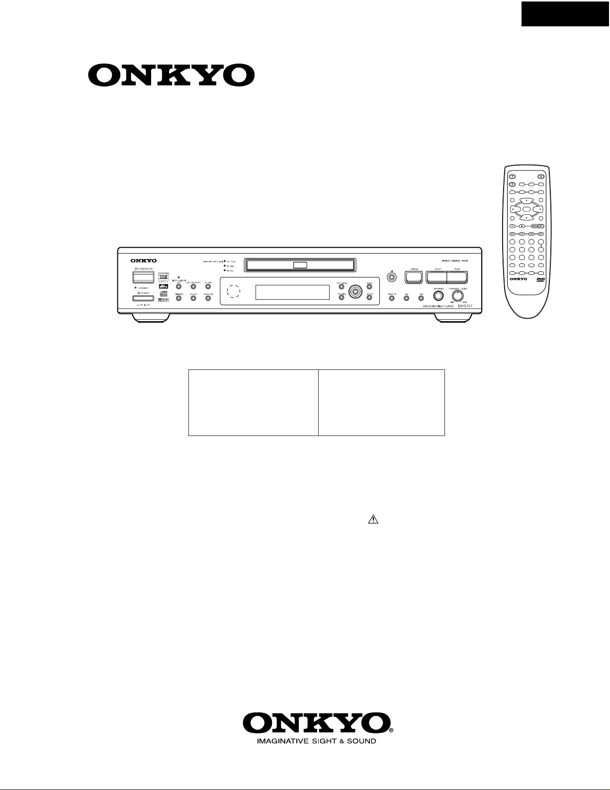
SERVICE MANUAL
DV-S757
Ref. No. 3697
082001
DVD AUDIO/VIDEO PLAYER
MODEL DV-S757
DIGITAL
SURROUND
ON
OPEN
STANDBY
ANGLE AUDIO
LAST M COND. M DIMMER DISPLAY
TOP MENU
ENTER
RETURN
STOPPAUSE
PLAY
DOWN UPFR FF
23
1
456
789
SEARCH
+
10
0
RANDOM REPEAT A-B
-
450
DV
RC
REMOTE CONTROLLER
/
CLOSE
SUBTITLE
MENU
SETUP
STEP/ SLOW
+
-
FUNCTION M
CLEAR
PROGRAM
RC-450DV
Black, Silver and Golden models
(B)MUP2P, (S)MUP2P
(G)MUT3P
100-240V AC, 50/60Hz
(B)MUS4P,(G)MUS4P
(G)MUR6P
SAFETY-RELATED COMPONENT
WARNING!!
COMPONENTS IDENTIFIED BY MARK ON THE
SCHEMATIC DIAGRAM AND IN THE PARTS LIST ARE
CRITICAL FOR RISK OF FIRE AND ELECTRIC SHOCK.
REPLACE THESE COMPONENTS WITH ONKYO
PARTS WHOSE PART NUMBERS APPEAR AS SHOWN
IN THIS MANUAL.
MAKE LEAKAGE-CURRENT OR RESISTANCE
MEASUREMENTS TO DETERMINE THAT EXPOSED
PARTS ARE ACCEPTABLY INSULATED FROM THE
SUPPLY CIRCUIT BEFORE RETURNING THE
APPLIANCE TO THE CUSTOMER.
Page 2
SPECIFICATIONS
DVD Player
Power supply AC 100-240 V, 50/60 Hz
Power consumption 15 W
Weight 3.4 kg, 7.5 lbs.
External dimensions
Signal system
Regional restriction code Some Asian area: 3
Laser Semiconductor laser, wavelength 650 nm
Frequency range (digital audio) DVD linear sound: 48 kHz sampling 4 Hz to 22 kHz
Signal-to-noise ratio (digital audio) More than 100 dB
Audio dynamic range (digital audio) More than 96 dB
Harmonic distortion (digital audio) Less than 0.015 %
Wow and flutter Below measurable level (less than ±0.001 % (W.PEAK)
Operating conditions
435 91 312 mm
PAL/AUTO
South American area: 4
Chinese area: 6
Audio CD: 4 Hz to 20 kHz
Temperature: 5 C to 35 C (41 F to 95 F), Operation status: Horizontal
(W/H/D), 17-1/8" 3-9/16" 12-5/16"
96 kHz sampling 4 Hz to 44 kHz
DV-S757
Outputs
Video output 1.0 V (p-p), 75 , negative sync., pin jack
S-video output (Y) 1.0 V (p-p), 75
(C) 0.286 V (p-p), 75
Component video output (Y) 1.0 V (p-p), 75 , negative sync., pin jack 1
B)/(PR)0.7 V (p-p), 75
(P
Audio output (digital output Optical) Optical connecter
Audio output (digital output Coaxial)
Audio output (analog audio)
Audio output (5.1 channel analog audio)
Specifications and features are subject to change without notice.
0.5 V(p-p),
2.0 V
2.0 V (rms), 470 , pin jack (FRONT L, FRONT R, CENTER, SURR L,
SURR R, SUB WOOFER) 1
75 , pin jack 1
470
(rms),
, negative sync., Mini DIN 4-pin
2
, pin jack (L, R) 2
2
2
Page 3
SERVICE PROCEDURES-1
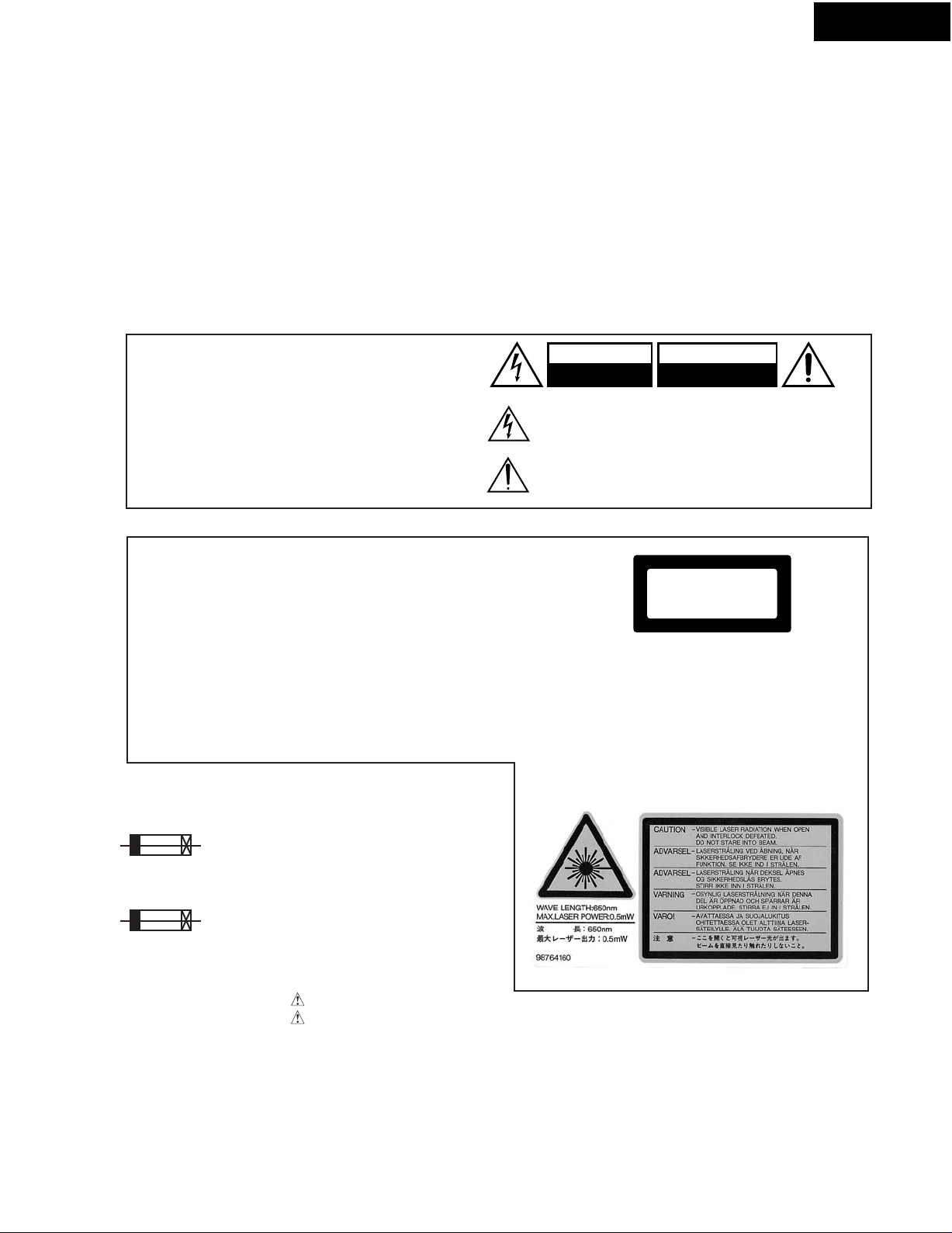
PROTECTION OF EYES FROM LASER BEAM DURING SERVICING
This set employs a laser. Therefore, be sure to follow
carefully the instructions below when servicing.
WARNING!!
SERVICE WARNING : DO NOT APPROACH THE
LASER EXIT WITH THE EYE TOO CLOSELY.
IN CASE IT IS NECESSARY TO CONFIRM LASER
BEAM EMISSION, BE SURE TO OBSERVE FROM
A DISTANCE OF MORE THAN 30cm FROM THE
SURFACE OF THE OBJECTIVE LENS ON THE
OPTICAL PICKUP BLOCK.
WARNING
Laser Diode Properties
CD
Wavelength:
Laser output:
650 nm
0.43 mW
DVD
Wavelength:
Laser output:
780 nm
0.14 mW
DV-S757
WARNING:
TO REDUCE THE RISK OF FIRE OR ELECTRIC SHOCK,
DO NOT EXPOSE THIS APPLIANCE TO RAIN OR
MOISTURE.
CAUTION:
TO REDUCE THE RISK OF ELECTRIC SHOCK, DO NOT
REMOVE COVER (OR BACK). NO USER-SERVICEABLE
PARTS INSIDE. REFER SERVICING TO QUALIFIED
SERVICE PERSONNEL.
LASER W ARNING
This unit contains a semiconductor laser system and is classified
as a "CLASS 1 LASER PRODUCT". So, to use this model
properly, read this Instruction Manual carefully. In case of any
trouble, please contact the store where you purchased the unit.
To prevent being exposed to the laser beam, do not try to open
the enclosure.
CAUTION:
VISIBLE LASER RADIATION WHEN OPEN AND INTERLOCK
FAILED OR DEFEATED. DO NOT STARE INTO BEAM.
CAUTION:
THIS PRODUCT UTILIZES A LASER. USE OF CONTROLS OR
ADJUSTMENTS OR PERFORMANCE OF PROCEDURES
OTHER THAN THOSE SPECIFIED HEREIN MA
HAZARDOUS RADIATION EXPOSURE.
Y RESULT IN
SERVICE PROCEDURE
1. Replacing the fuses
WARNING
RISK OF ELECTRIC SHOCK
DO NOT OPEN
The lightning flash with arrowhead symbol, within an equilateral
triangle, is intended to alert the user to the presence of uninsulated
"dangerous voltage" within the product's enclosure that may be of
sufficient magnitude to constitute a risk of electric shock to persons.
The exclamation point within an equilateral triangle is intended to alert
the user to the presence of important operating and maintenance
(servicing) instructions in the literature accompanying the appliance.
The label on the right
is applied on the rear
panel except for USA
and Canadian
models.
1.This unit is a CLASS 1 LASER PRODUCT and employs a
laser inside the cabinet.
2.To prevent the laser from being exposed, do not remove
the cover. Refer servicing to qualified personnel.
LASER BEAM CAUTION LABEL
"CLASS 1 LASER
PRODUCT"
AVIS
RISQUE DE CHOC ELECTRIQUE
NE PAS
OUVRIR
This symbol located near the fuse indicates that the
fuse used is show operating type, For continued protection against
fire hazard, replace with same type fuse , For fuse rating, refer to
the marking adjest to the symbol.
Ce symbole indique que le fusible utilise est e lent.
Pour une protection permanente, n'utiliser que des fusibles de meme
type. Ce demier est indique la qu le present symbol est apposre.
REF. NO.
F1
PART NO.
252073 or 1.6A-SE-EAK IECFUSE
DESCRIPTION
252273 1.6A-SE-TL250V
2. Safety-check out
(Only U.S.A. model)
After correcting the original service problem perform the
following safety check before releasing the set to the customer
Connect the insulating-resistance tester between the plug of
power supply cord and terminal GND on the back panel.
Specifications: More than 10M ohm at 500V
Page 4
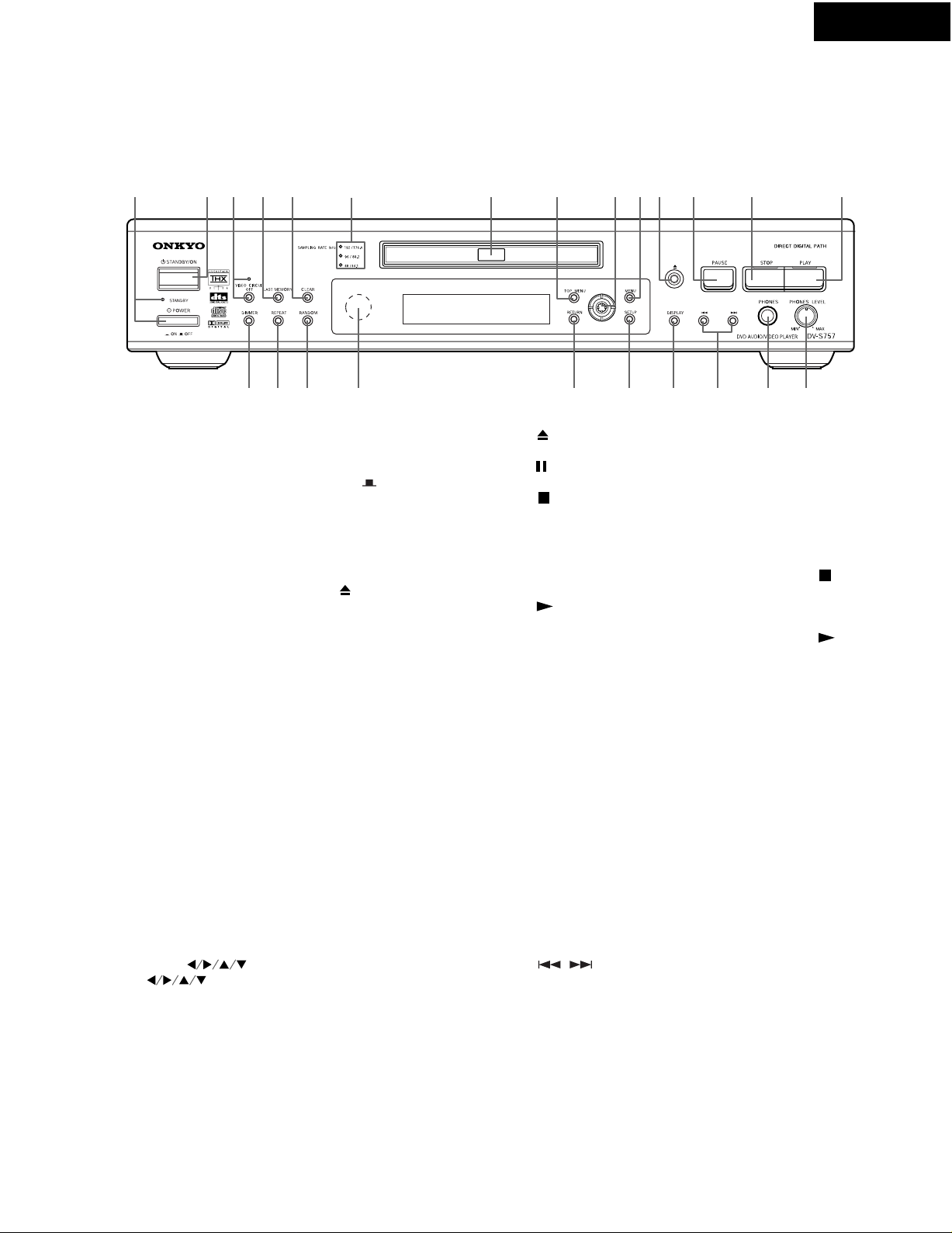
P ANEL VIEW -1
FRONT PANEL
1 2 3 4 5 6 7 8 9 10 11 12 13 14
15 16 17 18 19 20 21 22 23 24
DV-S757
1. POWER switch and STANDBY indicator
Turns on the main power supply for the DV-S757. The DV-S757
enters standby state and the STANDBY indicator lights up.
Pressing the switch again to the off position ( OFF) shuts down
the main power supply into the DV-S757.
Before turning on the power, make sure all cables are properly
connected.
2. STANDBY/ON button
When STANDBY/ON button is pressed to ON while the POWER
switch is set to ON, the DV-S757 turns on and the STANDBY
indicator turns off. The indicator around button light up.
Pressing the button again returns the DV-S757
to the standby state. This state turns off the display, disables
control functions.
3. VIDEO CIRCUIT OFF button and indicator
Press to switch the video signal off.
4. LAST MEMORY button
You can resume DVD or Video CD playback from the point you
last watched even if the disc is removed from the player. Press
LAST MEMORY during playback to set a Last Memory point.
When you want to resume playback of that disc, press LAST
MEMORY in the stop mode and playback starts from the
memorized point. Last Memory locations can be stored for up to 5
DVDs and 1 Video CD.
5. CLEAR button
Works in conjunction with a number of player functions. Use to
cancel repeat and random playback, and to edit programs.
7. Disc tray
When loading a disc, place discs in the disc tray with the label
side facing up.
8. TOP MENU button
Press to call up the top menu programmed on the DVD.
Depending on the DVD, the top menu may be identical to the
DVD menu.
9. Cursor ( ) button/ENTER button
Use to move through the options on menu screens and
to change settings. Use ENTER to implement settings selected
with the cursor buttons or to set items highlighted in a menu.
10. MENU button
Use to display or close the DVD menu or MP3 Navigator screen.
11. button
Press to open and close the disc tray.
12. PAUSE button
Press during playback to pause. Press again to resume playback.
13. STOP button
Press to stop playback. Pressing once enables playback to
resume from a point shortly before the location where it stopped.
Pressing twice causes the disc to return to the beginning of the
disc if playback starts again.
Whenever a disc is loaded in the player, indicator above STOP
lights up.
14. PLAY button
Press to start or resume playback.
Whenever a disc is loaded in the player, indicator above PLAY
lights up.
15. DIMMER button
Toggle to control the lightness of the display (3 steps).
16. REPEAT button
Use to set the repeat mode.
17. RANDOM button
Press to play chapters/tracks in random order.
18. Remote control sensor
Point the remote control toward the remote sensor to operate the
player.
19. RETURN button
Use to go one menu back (current settings are maintained). Use
RETURN when you do not want to change the option setting in a
menu.
20. SETUP button
Press when the player is in either play or stop mode to open and
close the Setup screen.
21. DISPLAY button
Press during playback to display statistical disc information.
Press repeatedly to display different information.
22. button
Press to go back or advance to previous chapters/tracks. Press
and hold to perform fast-reverse/fast-forward playback scanning.
23. PHONES jack
This is a standard stereo jack for connecting stereo headphones
The audio for the ANALOG OUTPUT CH 1 and CH 2 are sent to
the headphone speakers.
24. PHONES LEVEL dial
Use to control the phones level. Turn the dial clockwise to
increase the phones level and counterclockwise to decrease it.
Page 5
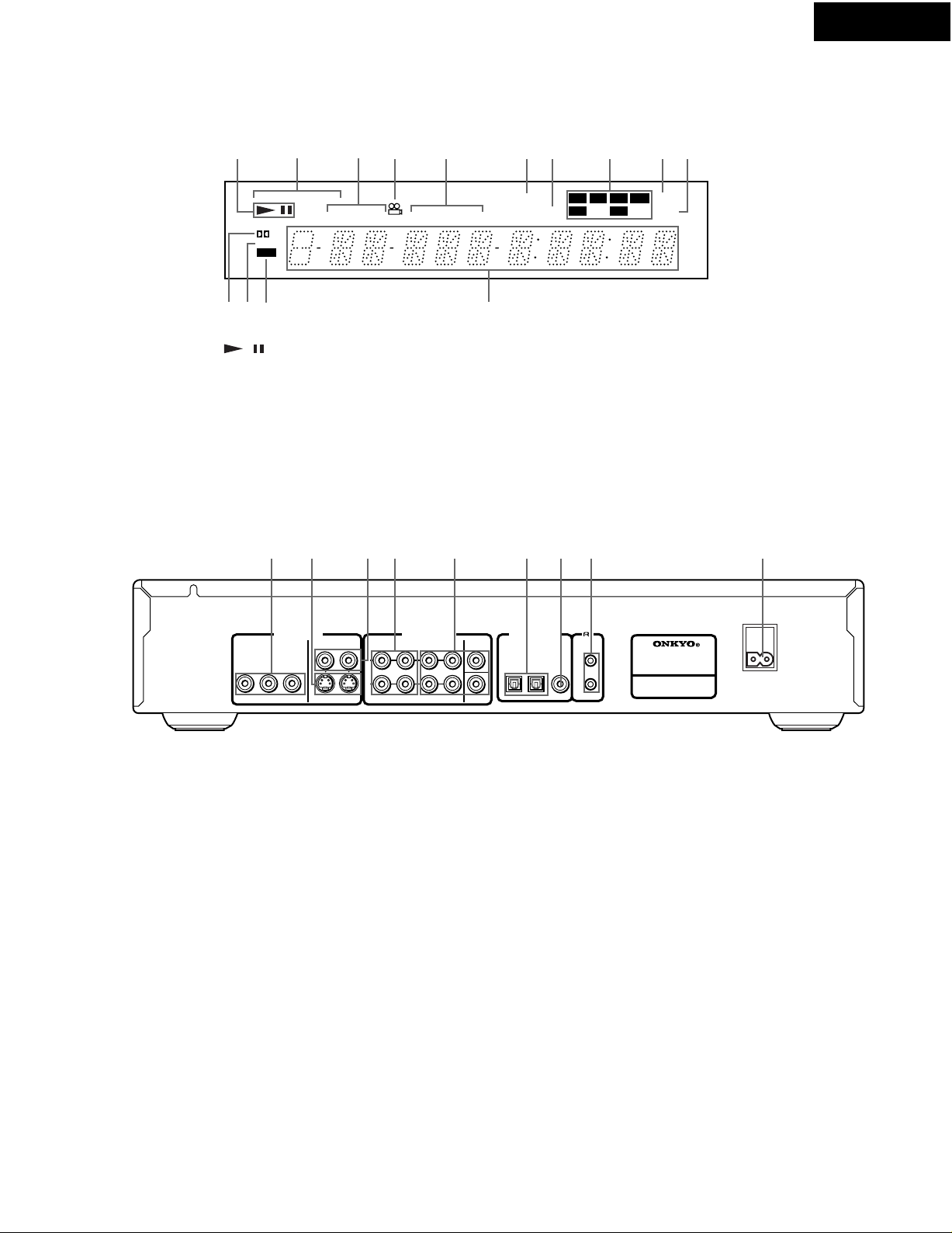
P ANEL VIEW -2
DISPLAY
1 2 3 4 5 6 7 8 9 10
DV-S757
11 12 13 14
1. / indicator
2. Inserted disc indicator
3. TITLE/GROUP indicator
4. Angle icon indicator
5. CHAPTER/TRACK indicator
6. REPEAT indicator
7. REMAIN indicator
REAR PANEL
DVD- AUDIOVC D
D
DTS
GUI
TITLE GROUP CHAPTER TRACK REMAIN
REPEAT
LAST
R LFECL
RSLS
COND.D.MIX
8. L, C, R, LS, RS, LFE and D.MIX indicator
9. LAST indicator
10. COND. indicator
11. D indicator
12. DTS indicator
13. GUI indicator
14. Multifunctional indicator
(e.g. operating status and error messages)
1 2 3 4 5 6 7 8 9
COMPONENT
Y
VIDEO OUTPUT
P
B
VIDEO
P
R
S VIDEO
L
R
CH 1
ANALOG OUTPUT
CH 2
FRONT
SURR
CENTER
SUB
WOOFER
DIGITAL OUTPUT
OPTICAL
COAXIAL
REMOTE
CONTROL
DVD AUDIO / VODEO PLAYER
MODEL NO.
DV-S757
AC INLET
1. VIDEO OUT COMPONENT jacks
If your TV or monitor has component video inputs, you can
produce a higher quality picture on your TV or monitor by
connecting to the component video outputs on this unit.
2. VIDEO OUTPUT S VIDEO jack
If your TV or monitor has an S-video input, clear picture
reproduction is possible by connecting the player to your TV or
monitor via the S-Video jack.
You can switch between [S1] and [S2] S-video output from the
Setup menu.
3. VIDEO OUTPUT VIDEO jack
Connect to the video input on a TV or monitor or AV amplifier or
receiver with video input capability.
4. ANALOG OUTPUT CH 1/CH 2 jacks
Use to output two-channel audio (analog) to the audio stereo
inputs on a TV or stereo amplifier.
5. ANALOG OUTPUT FRONT/SURR/CENTER/
SUBWOOFER jacks
Use to output 5.1 channel audio (analog) to the 5.1 channel
discrete inputs on an amplifier. If you are connecting to a receiver
that has both digital and analog input jacks for DVD player
connection, it may be beneficial to make both connections.
6. DIGITAL OUTPUT OPTICAL jack
Use to output the digital audio signal recorded on discs. You can
output the digital signal via the optical output jack to an AV
amplifier or receiver.
7. DIGITAL OUTPUT COAXIAL jack
Use to output the digital audio signal recorded on discs. You can
output the digital signal via the coaxial output jack to an AV
amplifier or receiver.
8. RI jack
Use to connect this player to another component bearing the .
mark. This lets you control this unit as though it were a
component in a system.
9.AC INLET
Use to connect the power cord to the wall outlet.
Page 6
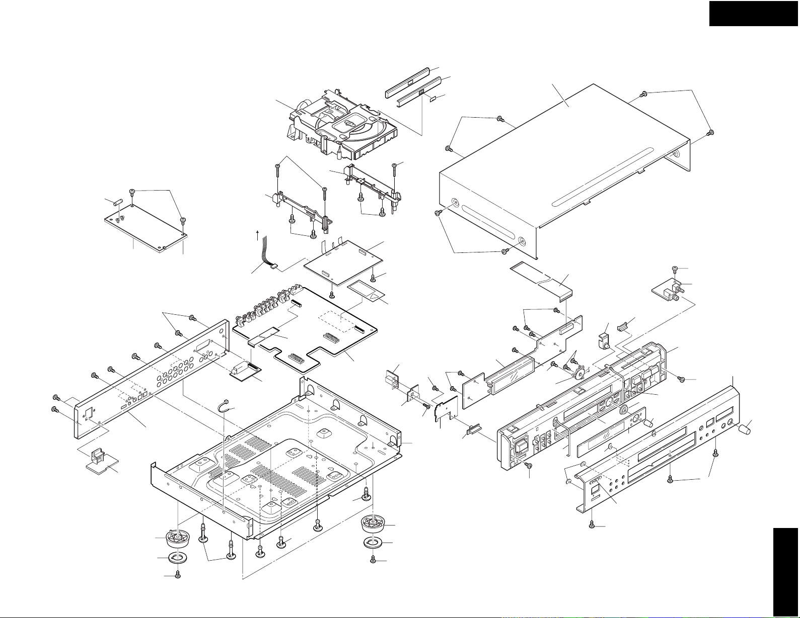
DV-S757
EXPLODED VIEW
F1
U11
59
61
U5
43
42
Z11
15
Z13
7
Z12
To DVD
Mechanism
E705
E903
7
7
E250
U9
U3
15
Z10
7
16
U4
U8
27
1
54
DVD
49
49
U1
7
7
U2
19
47
E701
7
28
29
S731
22
45
7
45
35
33
34
37
23
49
7
U10
21
41
7
22
36
59
13
3
3
5
9
7
11
5
7
53
59
DV-S757
Page 7

EXPLODED VIEW PARTS LIST-1
DV-S757
REF.NO. PART NO. DESCRIPTION
1
3
5
7
9
11
13
15
16
19
21
23
27
28
29
33
34
35
36
27100399A Chassis
27175316B Leg
28141332 Cushion
838130088 3TTB+8B, Self tapping screw
27190428A KGLS-10RF, Holder
27191112 KGPS-6RF, Holder
27190693 KGLS-6R, Holder
838130208 3TTB+20B, Self tapping screw
29362584
28325497A Knob, power <B>
28325499A Knob, power <G>
28325547A Knob power <S>
27111243 Front bracket <B>
27111244 Front bracket <S>
27111245 Front bracket <G>
28191926 Clear plate <B>
28191927 Clear plate <S,G>
82143010 3P+10FN(BC), Pan head screw
838126068 2.6TTB+6B, Self tapping screw
838426088 2.6TTB+8B(BC), Self tapping screw
28198935 Facet, PLAY
27268041 Guide, CRS
28325953 Knob B, OPEN AS <B>
28325954 Knob S, OPEN AS <S>
28325955 Knob G, OPEN AS <G>
28325452 Knob, MIC <B>
28325495 Knob, MIC <N,G>
28325515 Knob, MIC <S>
NOTE: THE COMPONENTS IDENTIFIED BY MARK ARE
CRITICAL FOR RISK OF FIRE AND ELECTRIC SHOCK.
REPLACE ONLY WITH PART NUMBER SPECIFIED.
!
Label DVD
REF.NO. PART NO. DESCRIPTION
37
41
42
43
45
47
49
53
54
59
<MUP> :European arer(Regional restriction code-2)
<MUT> :Some Asian arer(Regional restriction code-3)
<MUS> :South American arer(Regional restriction code-4)
<MUR> :Chinese arer(Regional restriction code-6)
<B> :Black color model only
<G> :Golden color model only
<S> :Silver color model only
28325933 Knob, CRS <B>
28325934 Knob, CRS <S>
28325935 Knob, CRS <G>
27212342A Front panel <B><MUP,MUS>
27212343A Front panel <S><MUP>
27212344A Front panel<G><MUS,MUT>
28148488 Door <B>
28148489 Door <S>
28148490 Door <G>
28148491 Door, MOULD <B>
28148492 Door, MOULD <S>
28148493 Door, MOULD <G>
28198906 Facet, S
28184779A Top cover <S>
28184780A Top cover <G>
28184808 Top cover <B>
838430088 3TTB+8B(BC), Self tapping screw <B>
838930088 3TTB+8B(UN), Self tapping screw <S,G>
28135244 Badge <B><MUP,MUS>
28135245 Badge <MUP,MUT,MUS>
28135245 Badge <G><MUR>
28135284 Badge, DVD-AUDIO <B>
28135285 Badge, DVD-AUDIO <S><G>
838430088 3TTB+8B(BC), Self tapping screw
NOTE:
DV-S757
Page 8

EXPLODED VIEW PARTS LIST-2
DV-S757
REF.NO. PART NO. DESCRIPTION
61
E250
E701
E705
E903
F1
S731
Z10
Z11
Z12
Z13
27122897B Rear panel <MUP>
27122898B Rear panel <MUT>
27122899B Rear panel <MUS>
27122900B Rear panel <MUR>
2047201512 NCFC7-201512, Flexible flat cable <MUP>
2045222012 NCFC5-222012, Flexible flat cable
2009990702UL NSAS-10P0978
260208 Binder, UL
252073 or 1.6A-SE-EAK IECFUSE
252273 1.6A-SE-TL250V
25035710 NPS-115-S673, Cursor switch ass'y
24150022 DB-VPB302, Main PC board ass'y
24801010 DB-VLD301-006, DVD mechanism ass'y
24840149A DB-VAC301, adapter(L)
24840150A DB-VAC302, adapter(R)
REF.NO. PART NO. DESCRIPTION
U1
U2
U3
U4
U5
U8
U9 1H465524-1B NAAR-7224-1B, Output terminal PC board ass'y <MUP>
U10 1H465525-1B NAETC-7225-1B, Phones jack PC board ass'y <MUP>
U11
1H465515-1B NADIS-7215-1B, Display PC board ass'y <MUP>
1H465515-1C NADIS-7215-1C, Display PC board ass'y <MUT>
1H465515-1D NADIS-7215-1D, Display PC board ass'y <MUS>
1H465515-1E NADIS-7215-1E, Display PC board ass'y <MUR>
1H465516-1B NADIS-7216-1B, Control switch PC board ass'y <MUP>
1H465516-1C NADIS-7216-1C, Control switch PC board ass'y <MUT>
1H465516-1D NADIS-7216-1D, Control switch PC board ass'y <MUS>
1H465516-1E NADIS-7216-1E, Control switch PC board ass'y <MUR>
1H465517-1B NAVD-7217-1B, AV connector PC board ass'y <MUP>
1H465518-1C NASW-7218-1C, Power switch PC board ass'y <MUT>
1H465518-1D NASW-7218-1D, Power switch PC board ass'y <MUS>
1H465518-1E NASW-7218-1E, Power switch PC board ass'y <MUR>
1H465519-1B NAPS-7219-1B, AC inlet PC board ass'y
1H465515-1B NAETC-7222-1B, Holder PC board ass'y
1H465524-1C NAAR-7224-1C, Output terminal PC board ass'y <MUS,MUT,MUR>
1H465525-1C NAETC-7225-1C, Phones jack PC board ass'y <MUS,MUT,MUR>
24150021A
NGPS-0021-100V-240V, Power supply unit <MUP, MUT, MUS, MUR>
NOTE: THE COMPONENTS IDENTIFIED BY MARK ARE
CRITICAL FOR RISK OF FIRE AND ELECTRIC SHOCK.
REPLACE ONLY WITH PART NUMBER SPECIFIED.
NOTE:
<MUP> :European arer(Regional restriction code-2)
<MUT> :Some Asian arer(Regional restriction code-3)
<MUS> :South American arer(Regional restriction code-4)
<MUR> :Chinese arer(Regional restriction code-6)
<B> :Black color model only
<G> :Golden color model only
<S> :Silver color model only
DV-S757
Page 9
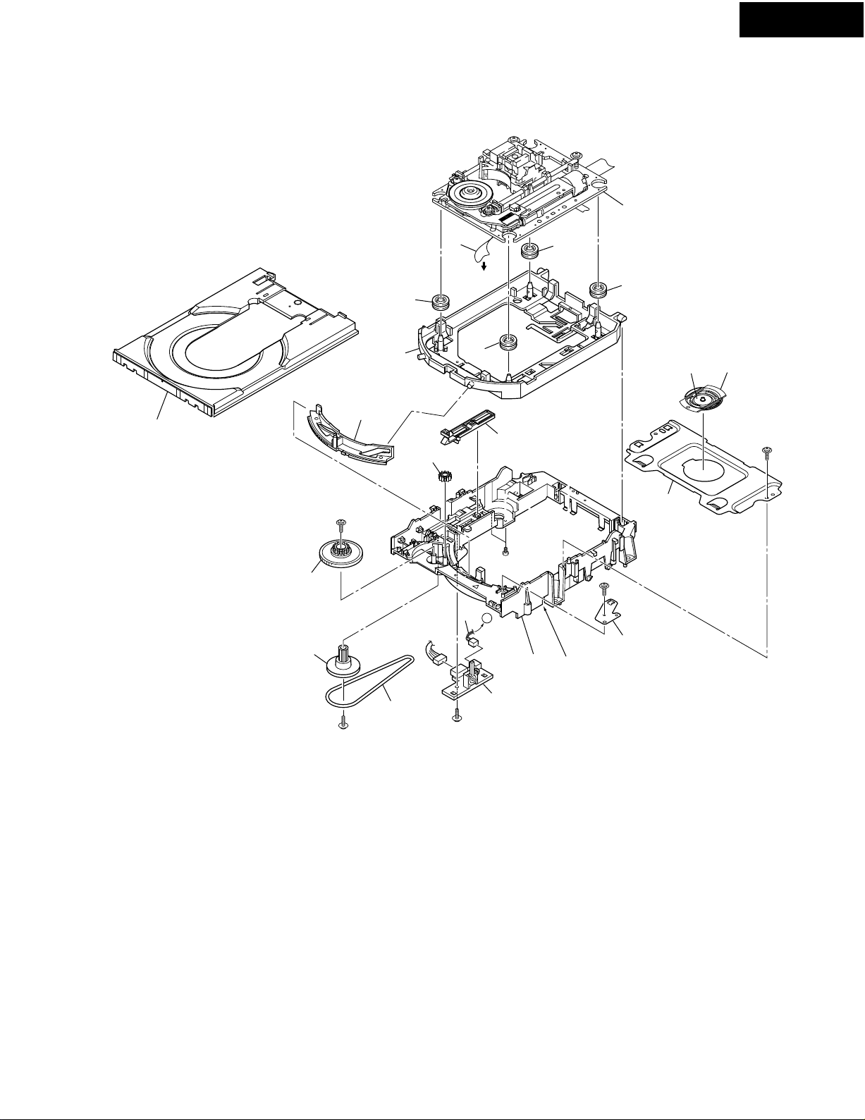
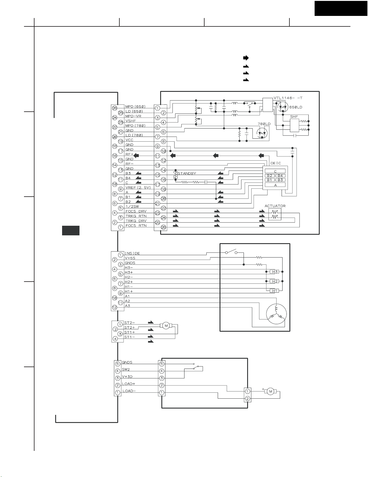
EXPLODED VIEWS OF MECHANISM
DVD MECHANISM : DB-VLD301-006
DV-S757
2
23
15
14
13
12
9
6
To DVDM
CN151
8
8
8
8
18
20
A
17
16
19
A
10
11
Lubricating Oil
GYA1001
1
PARTS LIST
REF.NO PART NO. DESCRIPTION REF.NO. PART NO. DESCRIPTION
1 VNP1836 Loading PC board assy
2 VXX2782 Traverse mechanism assy
6 VDA1864 Flexible cable 26P
8 VEB1327 Float rubber
9 VEB1328 Belt
10 VNE2253 Stabilizer
11 VNL1917 Loading base
12 VNL1918 Float base DVD
13 VNL1919 Drive cam
14 VNL1921 Gear pulley
15 VNL1922 Loading gear
16 VNL1923 Drive gear
17 VNL1925 SW lever
18 VNE2251 Clamper plate
19
20 VNL1924 Clamper
23 VNL1920
VNE2252
Bridge
Tray
Page 10
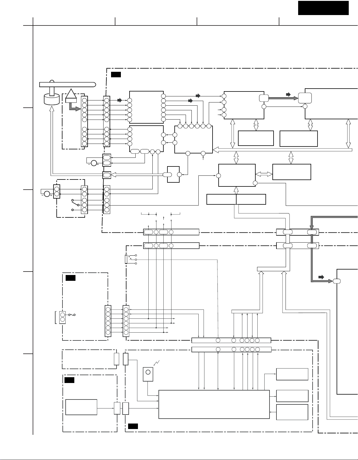
DV-S757
A
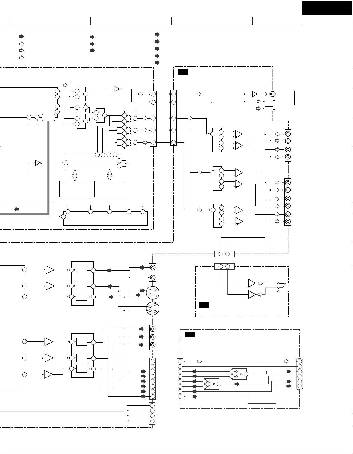
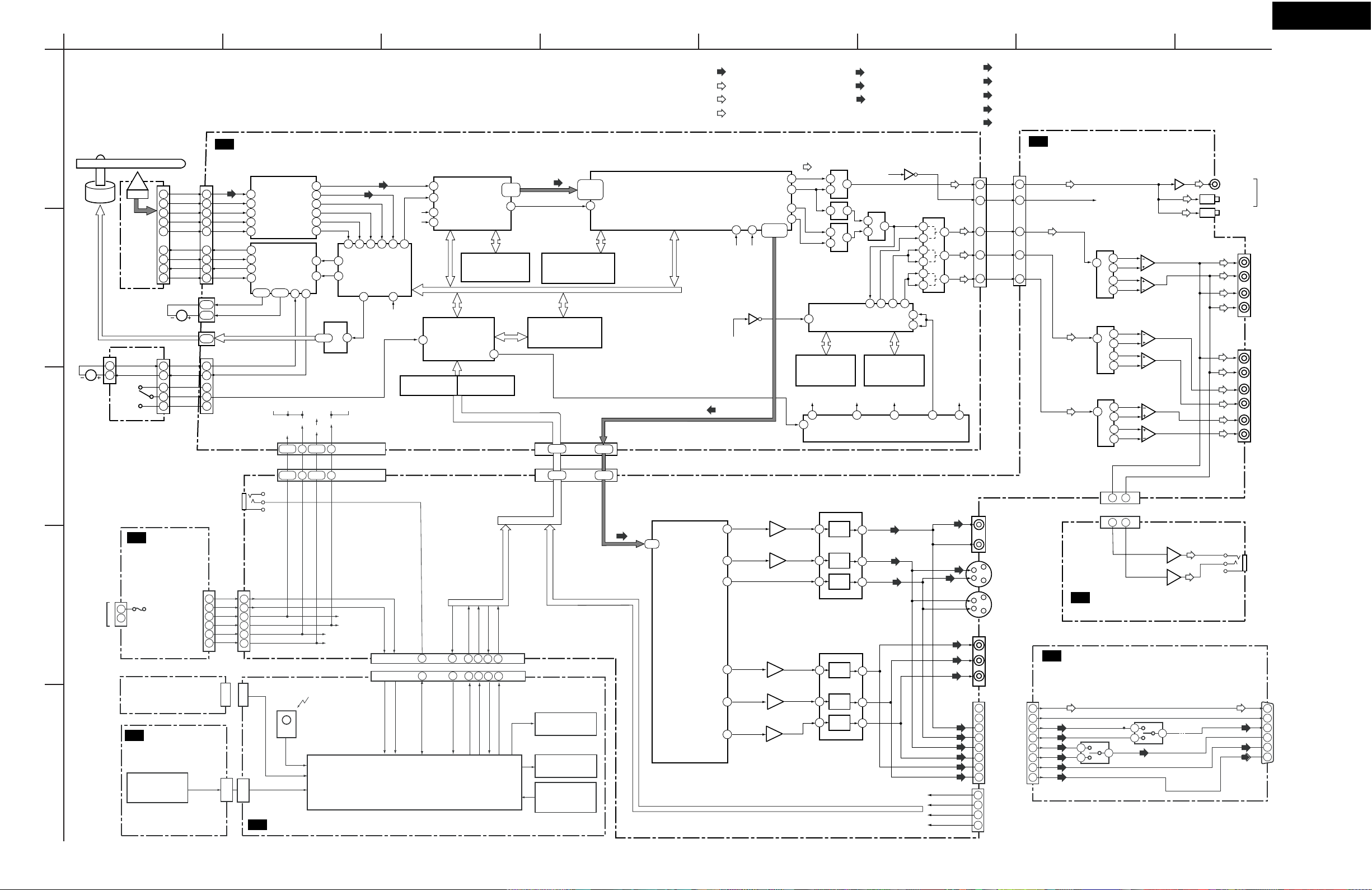
BLOCK DIAGRAMS-1
OVERALL
1
(24P)
Spindle
Motor
OEIC
PICKUP
ASSY
2
Carriage
Motor
CN601CN602
1
2
M
Loading
Motor
S101
Loading
Position
Switch
LOAB ASSY
3
11
20
21
15
16
25
24
23
26
1
2
3
4
5
RF
B1
B2
B3
B4
T DRV
T RTN
T DRV
F RTN
M
LOADLOAD+
V+3D
SW2
SW1(GNDS)
CN101
(24P)
11
20
21
15
16
25
24
23
26
CN104
1,2
3,4
CN105
4-9
CN103
1
2
3
4
5
Z10
MAIN BOARD ASSY
(RF)
RF
3
B1
B2
B3
B4
(12P)
LOD POS
IC101
6
LA9701M
7
RF IC
8
9
12
IC351
13
M56788AFP
9
10
DRIVER
34,35
31,32
FTS
V+6M
BCDEFGH
(RF)
BD0-BD7
CDDATA
IC802
HY57V161610DTC-8
16M SDRAM
IC603 VYW1835
8M FLASH
MEMORY
1-10
149,150,
152-155,
158,159
48
16-23
CN501
(40P)
IC801
M65774BFP
MPEG2
DECODER
AV-1
PD0-PD7
5,7
15 14
V+5DV+5VV+5S
SW+5
2 22
RFO
54
DSP RF
46
BH
56
PH
57
FE
42
TE
35
FDO
47
3
TDO
48
20
9-14
IC251
BA6664FM
SPDL
DRIVER
V+12D V+12M
V+3D
V12M
V3VD
8,10
(RF)
(RF)
32 33 30 31 39 3
IC201
LC78652W
SERVO DSP
46 14
SPDO
21
16M
LOD POS
CN401 (2/2)
AIN
170
ROMXA
112
33M
4
16M
107
57
CONTROL CPU
3.3V to 5V
CONVERTER
(30P)
IC701
PE5220A
DVD DECODER
BY CHIP
(SCRUT)
IC702
GM71VS65803CLT-5
64M DRAM
IC601
PD6345A
SYSTEM
105
5V to 3.3V
CONVERTER
57-60
63-66
44´48
111
2
9
CN302 (2/2)
1-10
16-23
CN601
(40P)
PD0-PD7
(VD)
1-8
U11
POWER SUPPLY
RI
REMOTE
CONTROL
P301
5,7 8,10
UNIT
CN2
(14P)
4
AC IN
1
F1
2
S731
CURSOR SWITCH
OPERATION SWITCH
U2
PC BOARD
NADIS-7216
14
10
8
6
4
2
5
OPERATION
SWITCH
JL771B
(5P)
-27V
EV+5V
+6V
+12V
+5V
+3.3V
P901
(14P)
14
10
8
6
4
2
P731
JL771A
(5P)
-27V
EV+5V
Q705
REMOTE
SENSOR
V+6M
V+12V
V+5V
V+3V
P701A
P701B
(22P)
(22P)
EV+5V
EV+5V
Q701
MPD780232GC
MICRO PROCESSOR
(FL DRIVER)
-27V
-27V
RI
12
12
SYS IN /OUT
Q102ADV7190KST
VIDEO
ENCODER
LT
XRADY
SO
SI
SCK
13
5
9
1
3
13
5
9
1
3
INDICATOR
SCK
SI
SO
P ON
LT
Q702
FL TUBE
OPERATION
SWITCH
U1 DISPLAY PC BOARD NAAR-7224
Page 11
DV-S757
AV-1
(RF)
: RF SIGNAL ROUTE
(AD)
: AUDIO DATA SIGNAL ROUTE
: AUDIO SIGNAL ROUTE
(D)
: AUDIO (DIGITAL) SIGNAL ROUTE
74
73
71
68
95-98,
6455
100-103
27M
(VD)
TC7SH04FU
27MDSP
36/16M
IC913
24
PD0-PD7
(For IC801,IC913) (For IC201,IC701)
44´48
(VD)
(V)
(D)
DOUT0
DOUT1
IC491
TC74VHC153FT
4
7
3
IC904
LC89051V
1 23
AO0
1
AO1
55
IC61LV6416-12T
27M
3
14
5
2
IC905
TC7WH157FU
IC901 XCA56367PV150
DVD AUDIO DSP
IC902
16M
13
IC481 BU2288FV
CLOCK GENERATOR
: VIDEO DATA SIGNAL ROUTE
: VIDEO SIGNAL ROUTE
: V SIGNAL ROUTE
IC401
TC7SH04FU
22/24M
24
IC906
TC74VHC157FT
2
4
3
SDI1
SDO0
SDO1
SDO2
65410
IC903
IC63LV1024-12T
36/16M
9
CN401(1/2)
3
2
5
6
10
11
IC908
TC74VHC157FT
16
22/24M
28
22/24M
10
(D)
(AD)
4
(AD)
7
(AD)
9
(For IC701)(For IC801)
33M
15
(Y)
(C)
(R)
(G)
(B)
(40P)
25
18
36
31
33
: Y SIGNAL ROUTE
: C SIGNAL ROUTE
: R SIGNAL ROUTE
: G SIGNAL ROUTE
: B SIGNAL ROUTE
U9
CN302(1/2)
(40P)
DOUT
25
DACCLK
18
DATA0
36
DATA1
31
DATA2
33
OUTPUT TERMINAL PC BOARD
NAAR-7224
Q403
NJM4565M-D
Q404
Q503
NJM4565-M-D
2
3
5
6
Q504
NJM4565M-D
Q504
NJM4565M-D
1
7
Q604
NJM4565M-D
Q302
(AD)
(D)
(AD)
(AD)
DACCLK
Q401
CS4392-KS
19
3
18
15
14
Q501
CS4392-KS
19
3
18
15
14
Q601
CS4392-KS
19
3
18
15
14
NJM4565M-D
P302
(D)
(D)
(D)
COAXIAL
DIGITAL OUT
OPTICAL
P401
L
CH-1
R
L
CH-2
R
P402
L
FRONT
R
L
SURROUND
R
SUB WOOFER
CENTER
45
41
44
36
40
37
AD-V
AD-C
AD-YS
AD-YD
AD-CB/B
AD-CR/R
Q801
TK15420M
(1/2)
Q801
TK15420M
(2/2)
Q805
TK15420M
(1/2)
Q805
TK15420M
(2/2)
Q809
TK15420M
(2/2)
IQ816 LA7106MFP
VIDEO AMP
V
3
AMP
15
C
6
AMP
13
Y
10
AMP
11
Q817 LA7106MFP
VIDEO AMP
3
AMP
15
6
AMP
13
10
AMP
11
46
V
(V)
C
(C)
(Y)
Y
(V)
(C)
(Y)
P801
VIDEO
S VIDEO
46
Q471
NJM4650D-D
U10
PHONES JACK PC BOARD
P472
PHONES
NAETC-7225
P250A
P351
P802
Y(GRN)
PB(BLU)
PR(RED)
P250B
(20P)
16
18
7
5
3
13
9
11
1
2
FOR UPGRADE FIRMWARE
3
4
AUDIO_L
AUDIO_R
18
V
7
Y
5
C
3
R
13
G
9
B
11
U3
AV CONNECTOR PC BOARD
NAVD-7217
MUP Type only
(V)
(Y)
(C)
1
(R)
2
(G)
(B)
Q251
TC4053BF
5
3
(R/C)
15
Q251
TC4053BF
4
(V/Y)
(G)
(B)
P251
(21P)
AV
CONNECTOR
L OUT
316
Audio
R OUT
1
V/Y OUT
19
R/C OUT
15
G OUT
11
B OUT
7
(G)
(B)
(R)
(V)
(Y)
(C)
(R)
(G)
(B)
TXD
RXD
DTR
CTS
Page 12
DV-S757
A
BLOCK DIAGRAMS-2
MECHANISM SECTION
1
CN101
2
Z10
3
MAIN BOARD
CN105
BCD
(RF)
(RF)
: RF SIGNAL ROUTE
: RF SIGNAL ROUTE
(F)
(F)
: FOCUS SERVO LOOP LINE
: FOCUS SERVO LOOP LINE
(T)
(T)
: TRACKING SERVO LOOP LINE
: TRACKING SERVO LOOP LINE
(S)
(S)
: SLIDER SERVO LOOP LINE
: SLIDER SERVO LOOP LINE
PICKUP ASSY
(RF) (RF) (RF) (RF)
(F)
(F)
(T)
(T)
(F)
(F)
(F)
(T)
(T)
(F)
(F)
(F)
(T)
(T)
(F)
(F)
(F)
(T)
(T)
(F)
(F)
(T)
(T)
(F)
SPINDLE MOTOR
STEPPING MOTOR
(CARRIAGE)
4
CN104
CN103
(S)
(S)
(S)
(S)
S101
: VSK1011
CN602
CN601
S5B-PH-K
S2B-PH-K
LOADING
MOTOR
ASSY
: VXX2505
5
LOAB ASSY
Page 13
DV-S757
A
BLOCK DIAGRAMS-1
OVERALL
1
(24P)
Spindle
Motor
OEIC
PICKUP
ASSY
2
Carriage
Motor
CN601CN602
1
2
M
Loading
Motor
S101
Loading
Position
Switch
LOAB ASSY
3
11
20
21
15
16
25
24
23
26
1
2
3
4
5
RF
B1
B2
B3
B4
T DRV
T RTN
T DRV
F RTN
M
LOADLOAD+
V+3D
SW2
SW1(GNDS)
CN101
(24P)
11
20
21
15
16
25
24
23
26
CN104
1,2
3,4
CN105
4-9
CN103
1
2
3
4
5
Z10
MAIN BOARD ASSY
(RF)
RF
3
B1
B2
B3
B4
(12P)
LOD POS
IC101
6
LA9701M
7
RF IC
8
9
12
IC351
13
M56788AFP
9
10
DRIVER
34,35
31,32
FTS
V+6M
BCDEFGH
(Y)
: Y SIGNAL ROUTE
(C)
: C SIGNAL ROUTE
(R)
: R SIGNAL ROUTE
(G)
: G SIGNAL ROUTE
(B)
: B SIGNAL ROUTE
U9
OUTPUT TERMINAL PC BOARD
NAAR-7224
CN302(1/2)
(40P)
(D)
(AD)
(AD)
(AD)
(For IC701)(For IC801)
33M
DOUT
25
DACCLK
18
DATA0
36
DATA1
31
DATA2
33
15
(40P)
25
18
36
31
33
(AD)
(D)
(AD)
(AD)
DACCLK
Q401
CS4392-KS
19
3
18
15
14
Q501
CS4392-KS
19
3
18
15
14
Q601
CS4392-KS
19
3
18
15
14
NJM4565M-D
NJM4565M-D
Q403
NJM4565M-D
Q404
Q503
NJM4565-M-D
2
3
5
6
Q504
Q504
NJM4565M-D
1
7
Q604
NJM4565M-D
Q302
(D)
(D)
P302
(D)
COAXIAL
DIGITAL OUT
OPTICAL
P401
L
CH-1
R
L
CH-2
R
P402
L
FRONT
R
L
SURROUND
R
SUB WOOFER
CENTER
5,7
15 14
V+5DV+5VV+5S
SW+5
2 22
RFO
54
DSP RF
46
BH
56
PH
57
FE
42
TE
35
FDO
47
3
TDO
48
20
9-14
IC251
BA6664FM
SPDL
DRIVER
V+12D V+12M
V+3D
V12M
V3VD
8,10
(RF)
(RF)
32 33 30 31 39 3
IC201
LC78652W
SERVO DSP
46 14
SPDO
21
16M
LOD POS
CN401 (2/2)
AIN
170
ROMXA
112
33M
4
16M
107
57
CONTROL CPU
3.3V to 5V
CONVERTER
(30P)
IC701
PE5220A
DVD DECODER
BY CHIP
(SCRUT)
IC702
GM71VS65803CLT-5
64M DRAM
IC601
PD6345A
SYSTEM
105
5V to 3.3V
CONVERTER
57-60
63-66
44´48
111
BD0-BD7
CDDATA
(RF)
149,150,
152-155,
158,159
48
IC802
HY57V161610DTC-8
16M SDRAM
IC603 VYW1835
8M FLASH
MEMORY
1-10
16-23
CN501
(40P)
IC801
M65774BFP
MPEG2
DECODER
AV-1
PD0-PD7
(RF)
: RF SIGNAL ROUTE
(AD)
: AUDIO DATA SIGNAL ROUTE
: AUDIO SIGNAL ROUTE
(D)
: AUDIO (DIGITAL) SIGNAL ROUTE
74
73
71
68
95-98,
6455
100-103
27M
(VD)
TC7SH04FU
27MDSP
36/16M
IC913
24
PD0-PD7
(For IC801,IC913) (For IC201,IC701)
44´48
(VD)
(V)
(D)
DOUT0
DOUT1
IC491
TC74VHC153FT
4
7
3
IC904
LC89051V
1 23
AO0
1
AO1
55
IC61LV6416-12T
27M
3
14
5
2
IC905
TC7WH157FU
IC901 XCA56367PV150
DVD AUDIO DSP
IC902
16M
13
IC481 BU2288FV
CLOCK GENERATOR
: VIDEO DATA SIGNAL ROUTE
: VIDEO SIGNAL ROUTE
: V SIGNAL ROUTE
IC401
TC7SH04FU
22/24M
24
IC906
TC74VHC157FT
2
4
3
SDI1
SDO0
SDO1
SDO2
65410
IC903
IC63LV1024-12T
36/16M
9
CN401(1/2)
3
2
5
6
10
11
IC908
TC74VHC157FT
16
22/24M
28
22/24M
10
4
7
9
2
Q705
REMOTE
SENSOR
9
V+5V
V+3V
V+6M
V+12V
P701A
P701B
(22P)
(22P)
CN302 (2/2)
EV+5V
EV+5V
Q701
MPD780232GC
MICRO PROCESSOR
(FL DRIVER)
-27V
-27V
RI
12
12
SYS IN /OUT
1-10
LT
XRADY
SO
SI
SCK
13
5
9
1
3
13
5
9
1
3
INDICATOR
SCK
SI
SO
P ON
LT
Q702
FL TUBE
OPERATION
SWITCH
16-23
CN601
PD0-PD7
(VD)
(40P)
1-8
Q102ADV7190KST
VIDEO
ENCODER
45
41
44
36
40
37
AD-V
AD-C
AD-YS
AD-YD
AD-CB/B
AD-CR/R
Q801
TK15420M
(1/2)
Q801
TK15420M
(2/2)
Q805
TK15420M
(1/2)
Q805
TK15420M
(2/2)
Q809
TK15420M
(2/2)
IQ816 LA7106MFP
VIDEO AMP
V
3
AMP
15
C
6
AMP
13
Y
10
AMP
11
Q817 LA7106MFP
VIDEO AMP
3
AMP
15
6
AMP
13
10
AMP
11
46
V
(V)
C
(C)
(Y)
Y
(V)
(C)
(Y)
P801
VIDEO
S VIDEO
46
Q471
NJM4650D-D
U10
PHONES JACK PC BOARD
P472
PHONES
NAETC-7225
P250A
P351
P802
Y(GRN)
PB(BLU)
PR(RED)
P250B
(20P)
16
18
7
5
3
13
9
11
1
2
FOR UPGRADE FIRMWARE
3
4
AUDIO_L
AUDIO_R
18
V
7
Y
5
C
3
R
13
G
9
B
11
U3
AV CONNECTOR PC BOARD
NAVD-7217
MUP Type only
(V)
(Y)
(C)
1
(R)
2
(G)
(B)
Q251
TC4053BF
5
3
(R/C)
15
Q251
TC4053BF
4
(V/Y)
(G)
(B)
P251
(21P)
AV
CONNECTOR
L OUT
316
Audio
R OUT
1
V/Y OUT
19
R/C OUT
15
G OUT
11
B OUT
7
(G)
(B)
(R)
(V)
(Y)
(C)
(R)
(G)
(B)
TXD
RXD
DTR
CTS
5,7 8,10
RI
REMOTE
CONTROL
P301
U11
POWER SUPPLY
UNIT
CN2
(14P)
4
AC IN
1
F1
2
S731
CURSOR SWITCH
OPERATION SWITCH
U2
PC BOARD
NADIS-7216
14
10
8
6
4
2
-27V
EV+5V
+6V
+12V
+5V
+3.3V
14
10
8
6
4
2
P901
(14P)
P731
-27V
EV+5V
5
OPERATION
SWITCH
JL771B
(5P)
JL771A
(5P)
U1 DISPLAY PC BOARD NAAR-7224
Page 14
A
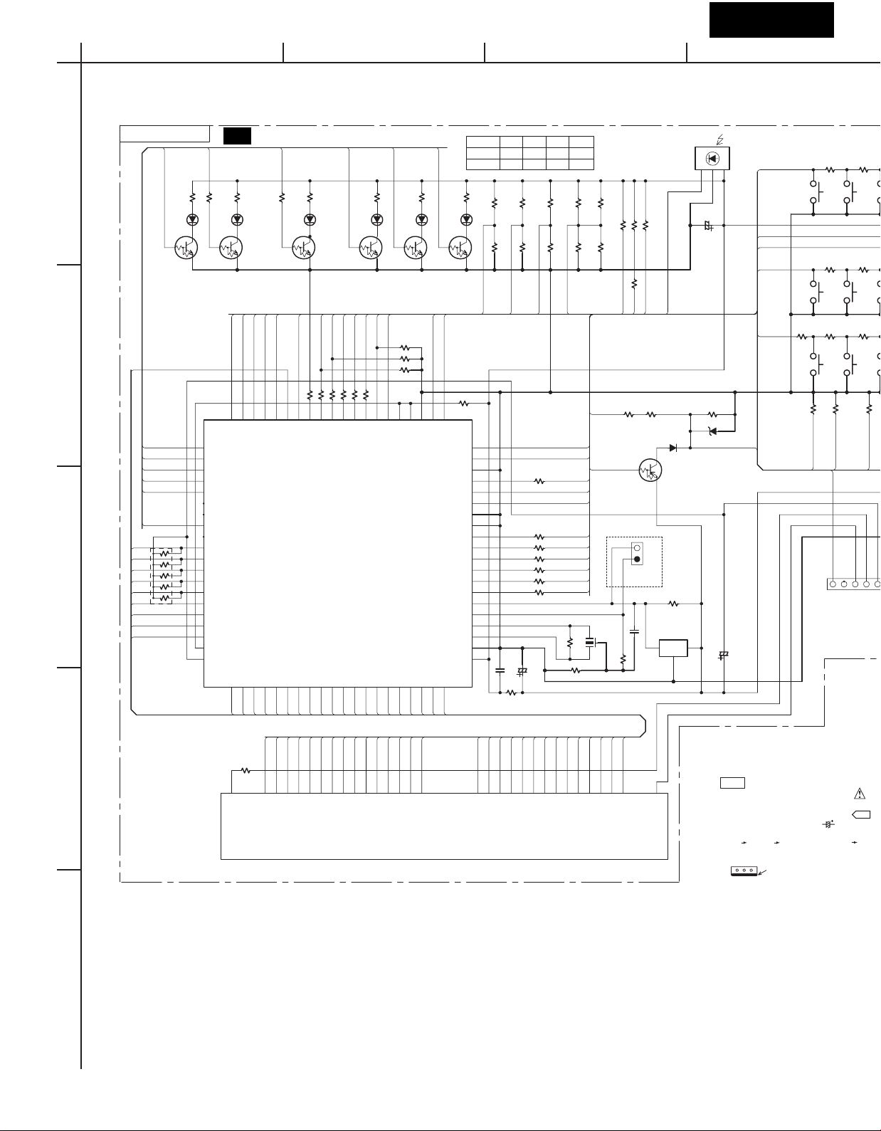
SCHEMATIC DIAGRAMS-1
BCDEFGH
NADIS-7215
1
OPC_L
Q706
RN1407
orKRC197S
2
192_L K2 RI
96_L INIT1
PLY_L SYSOUT
STP_L VCOFF
OPC_L LT1
48_L
P15 PON
P14 XRDY
3
P13 SO
P12 SI
P11 XSCK
P10
R785
P9
P8
P7
STP_L
100
R732
R058 0
D703
OPEN_LED
Q707
RN1407
FL_ON/OFF
DISPLAY PC BOARD
U1
100
R731
D704
STOP_LED
D703,D704,D705
SEL2E10C
STB_L
VOF_L
MSO_0
MSO_1
39
40
VLED
192LED41
MSO_0 38
96LED42
PLYLED43
STPLED44
OPCLED45
LEDO46
PAUSELED47
48LED48
POWERLED49
P1550
P1451
P1352
P1253
P1154
P1055
P956
P857
P758
VDD259
VLOAD60
MSO_1 37
STBYLED
P364
P463
P562
P661
P6P5P4P3P2
100
R7590
232SO
R7130
TEST 33
232SCK
R7120
R232SO 32
R232SCK 31
96_L
Q709
RN1407
232SI
R7110
R232SI 30
PLY_L
0
R057
PLAY_LED
Q708
RN1407
MSO_2
MSO_2 36
FL_ON/OFF 35
R730
D705
SRESET
R232RESET 34
Q701
MPD780232GC-047-8BT
10G71
11G70
12G69
13G68
14G67
P166
P265
P1
14G
13G
12G
11G
10G
R728
10K
R788
10K
R789
10K
R790
VDD0 25
5G76
470
D707
RN1407
orKRC107SorKRC107SorKRC107SorKRC107SorKRC107S
K0
+5V 24
VSS0 23
SYSRESET 12
3G78
4G77
48_L
192_LED
Q711
K0 22
2G79
192_L
470
R729
D706
96_LED
Q710
RN1407
D706,D707,D708
SEL4910D-D
232BU
232RE
SYSIN
SYSOUT
R7100
R7090
SYSIN 26
SYSOUT 27
R232REQ 28
R232BUSY 29
6G75
7G74
8G73
9G72
9G8G7G6G5G4G3G2G1G
R760
D708
K1
R052
K121
K2 20
INIT1 19
GND2 18
VCOFF 17
LT1 16
IRIN 15
NC2 14
NC1 13
PON 11
XRDY 10
SO 9
SI 8
XSCK 7
RESET 6
GND1 5
X1 4
X2 3
VSS1 2
VDD1 1
1G80
470
0
*R720
*R721
48_LED
MSO_0
C702
8.2k
5.6k
NC
R727
R7260R724
MSO_1
R708 0
R707 0
R706 0
R705 0
R704 0
R703 0
R702 0
R054
104Z
0
33k
R725NCR723
0
MSO_2
C701
100/6.3
NC
0
27k
68k5.6k
MURMUSMUTMUP
33k
5.6k
R722
INIT1
REMO
RESET
R701
*R721*R720
SYSIN
X701
5.00MHZ
1M
R053
0
NC
NC
Q705
REMOTE
SENSOR
PIC-37043TH2
R787
R717 2.7K
R718 2.7K
R719 2.7K
R786
0
R055
K0
K1
R715
47K
Q704
RN2403
orTRA103S
C706
223Z
10K
R782
K2
R051
0
P710A
Q712
BD4742G
REMO
D701
1SS352
R714
4.7K
G
C704
100/6.3
R716 220K
D702
UDZS5.6B
IO
C703
22/50
K0
STB_L
VOF_L
K1
K2
R747
390
S712
CLEAR
R733
390
S701
T.MENU
R0560R740
390
S709
PAUSE
NC
R752
R755
232RE
SRESET
P701B
R748
RANDOM
R734
MENU
R741
STOP
NC
232BU
FLAC2
NC 21
SRESET 22
470
S713
470
S702
470
S710
R753
FLAC1
FLAC2 20
REPEAT
SETUP
PLAY
NC
232SI
-27V
-27V 18
FLAC1 19
P9
P8
P7
P10 39
P8 37
P9 38
P6P5P4P3P2
P6 35
P7 36
P15
P14
P13
P12
P11
P10
P11 40
P12 41
P13 42
P14 43
4
R060
F1 48
0
P15 44
P1
P1 30
P2 31
P3 32
P4 33
P5 34
Q702 14-BT-68GNK
14G
14G18
13G
13G17
9G8G7G6G5G4G3G2G1G
12G
11G
10G
8G 12
9G 13
10G14
11G15
12G16
NOTE
.
THE COMPONENTS IDENTFIED
REPLACE ONLY
.
7G 11
F2' 1
1G 5
2G 6
3G 7
4G 8
5G 9
6G 10
VOLTAGE (MEASURED WITHVOLTMETER) IS
.
ELECTROLYTIC CAPACITORS (
.
ALL CAPACITORS ARE IN pF/50WV UNLESS OTHERWISE NOTED.
EX) 030 3pF 330 33pF 331 330pF
.
ALL RESISTORS ARE IN OHMS 1/4WATTS
.
THE THICK LINES ON PC BOARD ARE THE PRINTING SIDE OF THE PARTS.
EX) PRINTING SIDE
.
CIRCUIT IS SUBJECT TO CHANGE FOR IMPROVEMENT.
WITH PART
NUMBER SPECIFIED.
ARE CRITICAL FOR SAFETY.
MARKBY
ARE IN F/WV.
u
)
333 0.033uF
UNLESS OTHERWISE NOTED.
5
Page 15
R749
R750
820
1K
S713
S714
R735
820
S703
R742
820
S711
S715
MEMORY
R736
1K
S704
RETURN
R743
1K
DISPLAY
REPEAT
S702
SETUP
PLAY
S710
R753
NC
232SI
RI
LT1
VCOFF
100
R754
GND
GND
-27V
E+5V
FLAC1
-27V 18
E+5V 17
FLAC1 19
ARE CRITICAL FOR SAFETY.
DCVOLTAGE.
u
RI
LT1_1
VCOFF
RI 12
LT1 13
GND1 16
GND2 14
VCOFF 15
to NAAR-7224
P701
(NO INPUT SIGNAL)
R737
1.8K
S705
R744
1.8K
RESET
RESET
232RE 10
RESET 11
R738
3.9K
DOWN
R745
3.9K
PON
PON
PON 9
232BU 8
U2
NADIS-7216
JL771B
JL771A
R739
10K
UP
S707
S706
R746
10K
R059
0
SO
XRDY
232SCK
SO
XRDY
232SCK
SO 5
232SI 6
XRDY 7
232SCK 4
to NAAR-7224
P250A
OPERATION SWITCH PC BOARD
R771
R772
1.8K
3.9K
R773
OFF
S721
S722
VIDEO
CIRCUIT
DIMMER
S723
STANDBY
D721
R041
Q721
0
RN1407
OPEN
ENTER
RIGHT
SI
100
R758
SI_1
S708
DOWN
UP
LEFT
XSCK
232SO
XSCK
232SO
P731
orKRC107S
7
6
5
4
3
2
1
ENTER
CURSOR
S731
RN1407
NPS-115-S673
CAUTION
VA
ATTENTION
VA
NAVD-7217
SI 3
232SO 2
SQUEEZE
SCK 1
+8V
AUDIO_R
GNDA
AUDIO_L
+5V
GND
GND
GND
GND
-5V
VSEL2
VVSEL1
V+12V
C251
100/16
20
19
18
17
16
15
14
R
13
12
B
11
10
G
9
8
V
7
6
5
Y
4
3
C
2
1
P250B
104Z
C252
104Z
100
22K
R267
R268
AUDIO_R
AGND
AUDIO_L
V+5V B1
R1
B1
G1
V1
Y1
C1
GND
C254
100/6.3
Q252
TC74HCT00AF
1
2
3
4
5
6
GND7
470
R774
D722
STANDBY
Q722
orKRC107S
470
VIDEO CIRCUIT_OFF
CN2
POWER SUPPLY UNIT
U11
GND2
GND3
SW+5V
SW+3.3V
to NAAR-7224
FOR CONTINUED PROTECTION
AGAINST FIRE HAZARD, REPLACE
ONLY WITH FUSE OF SAME TYPE
AND RATING INDICATED.
AFIN D'ASSURER UNE PROTECTION
PERMANENTE CONTRE LES RISQUES
D'INCENDIE, REMPLACER UNIQUEMENT
PAR UN FUSIBLE DE MEME TYPE
ET CALIBRATION COMME INDIQUE.
V+12V
C262
Q255
2SC2712
or KTC3875
104Z
C263
VCC14
13
12
11
10
9
8
R572
0
C265
100/6.3
C259
R273
R571
0
104Z
6.8K
R274
150K
Y11
Z13
Z4
Z05
EN6
VEE7
GND8
4.7K
R259
Q253 2SC2712
C260
104Z
5.1K
R275
10K
R276
Q251
TC4053BF
C253
100/16
22K
R260
R261
1K
or KTA1504
or KTC3875
VCC16
Y15Y02
X14
X1 13
X0 12
A11
B10
C9
R286
100
Q254
2SA1162
C264
R262
AC INLET PC BOARD
U5
NAPS-7219
NGPS-0021
F1
CN1
FUSE T1.6A 250V
GND1
SW+12V
M+5V
GNDM
GND0
EVER+5V
-27V
FLAC2
FLAC1
POWER_ON
P901
U4
THIS SYMBOL LOCATED NEAR THE FUSE INDICATES
THAT THE FUSE USED IS SLOW OPERATING TYPE
FOR CONTINUED PROTECTION AGAINST FIRE
HAZARD,REPLACE WITH SAME TYPE FUSE. FOR FUSE
RATING REFER TO THE MARKING ADJACENT TO THE SYMBOL
CE SYMBOLE INDIQUE QUE LE FUSIBLE UTLISE EST
E LENT. POUR UNE PROTECTION PERMANENTE,N'UTILISER
QUE DES FUSIBLES DE MEME TYPE. CE DARNIER EST
INDIQUE LA QU LE PRESENT SYMBOL EST APPOSE.
U3
Q259
4.7K
R278
2SD655
D252
1SS226
D252
470
R266
or KTC2874
R279
1K
1K
R280
Q258RN1402
or KRC102S
G1
B2
G2
R288
R287
R/C
470(1/2W)
Q261
V/Y
Q262
2SA933
or KTA1267
R263
150
R264
150
C261
104Z
C255
470/6.3
C256
470/6.3
470
C257
(1/2W)
470/6.3
2SA933
C258
470/6.3
Q260
2SD655
or KTC2874
R251
75
R253
75
R255
75
or KTA1267
R257
75
D251
1SS226
D251
1SS226
Q256
2SC2712
or KTC3875
1K
1SS226
104Z
R575 0 R277
R285
100
470
56K
R270
R265
23
12
470
P982B
P982
P982A
NASW-7218
POWER
P982C
P982D
POWER SWITCH PC BOARD
AV CONNECTOR PC BOARD
MUP2P Type Only
AV CONNECTOR
R574
0
R252
L251
BK1608LM182-T
R254
L252
BK1608LM182-T
R256
L253
BK1608LM182-T
R258
L254
BK1608LM182-T
DV-S757DV-S757
AC INLET
P981B
100-240V 50Hz/60Hz
S991
C991
103M
P251
AUDIO_R
1
2
AUDIO_L
3
AGND
4
VGND1
5
6
B
7
F.SW
8
VGND2
9
10
G
11
12
VGND3
13
VGND4
14
R/C
15
RGB.SW
16
VGND5
17
VGND6
18
CV/Y
19
20
VGND7
21
E201A
Page 16

DV-S757
A
SCHEMATIC DIAGRAMS-2
NC : No connecton
1
To POWER SUPPLY UNIT
CN2
2
to DVD MAIN BOARD
CN401
3
4
to NADIS-7215
P701B
5
P901
GND3 1
SW+3.3V_2 2
GND2 3
SW+5V 4
GND1 5
SW+12V 6
GNDM 7
M+5V 8
GND0 9
EVER+5V 10
POWER_ON 11
FLAC1 12
FLAC2 13
-27V 14
CN302
GNDM 1
5V 2
GNDM0 3
GND10 4
6V_2
GND9 6
6V_1 7
3.3V_2 8
12V 9
3.3V_1 10
GND8 11
2.5V_2 12
GND7 13
2.5V_1 14
GND6 15
GND5 16
GND4 17
DACCLK 18
NC1 19
GNG3 20
NC2 21
ZCSAQE 22
GND2 23
XAQRST 24
DOUT 25
XDFSO 26
XAMUTE 27
XDFSCK 28
XMMUTE 29
GND1 30
DATA1 31
BCK 32
DATA2 33
GND0 34
XCSDF1 35
DATA0 36
XFRST1 37
LRCK 38
XFRST0 39
XCSDF0 40
P701A
KESET
NC
FLAC1
FLAC2
-27V
EVER+5V
GND1
VCOFF
GND0
LT
RI
XRESET
232RE
P_ON
232UB
XRADY
232SI
SO
232SCK
SI
232SO
SCK
SW+12V
3.3
5.0
GND
GNDM
SW+5V
5.8
5
R301
0
R322 10K
22
21
20
19
18
17
16
15
14
13
12
11
10
9
8
7
6
5
4
3
2
1
BCDEFGH
D901
11.3
Q901
PQ025EZ5MZP
GND5NC
ON/OFF
VIN1VOUT
4
2
3
C915
C917
C919
C921
C923
R304
NC
R309
R311
R312
R314
R316
R318
R320
DOUT
RI
100/6.3
220/6.3
220/16
220/6.3
220/16
R305
0
0
0
0
0
0
0
0
R343
C904
DACCLK
Q301
32 1
NC
470
BK1608LM182-T
C901
104Z
5.0
C916
V+6M
R302
FLAC1
FLAC2
-27V
VCOFF
XRESET BCK
P_ON MCLK4 -B
XRADY
SCK
104Z
SW+12V
C918
104Z
C920
104Z
C922
104Z
104Z
C924
104Z
C925
R303 0
C301
L301
NC
NC
NC
R308
0
R310
0
R313
0
R315
0
R317
0
R319
0
R321
0
R325 10K
R324 10K
R323 10K
LT
RI DATA2 +B
SO
SI
78M08
Q902
C905
104Z
P_ON
FLAC2 +B
FLAC1
-27V AGND
EVER+5V
45
NC
C302
DOUT +B
XDFSO
XAMUTE
XDFSCK -B
XMMUTE
DATA1
BCK
DATA2
XCSDF1
DATA0
XFRST1
LRCK
XFRST0
XCSDF0
R342
P303BP303A
0
C303
NC
C314
223Z
L304
P301
RI
RL1N4003 OR GP1N4003E
IO
G
C906
100/16
R901
0
C930
BCK DATA1
0
MCK BCK
R002
104Z
223Z
C313
123
8.7
100/16
102
C911
45
Q904
NJM2374A
678
C913470/16
104
R903
0.47
(1/2W)
TC7SH86FU
Q004
321
33K
R005
10K
R001
C005
R330
100K
NC
C304
123
45
Q902,C906
MUP Type only
C907
100/16
R910
(1/2W)
8.2
0
R908
R902
0
V+3V
22
R004
Q001
TC7WH74FU
8
1
7
2
6
3
5
4
0
R003
R331
470K
Q302 TC74VHCUO4FT
1
2
3
4
5
6
GND7
C306 100/6.3
C307 104Z
C308 104Z
C309 100/6.3
U302 GF1FA551TZ
C908
NC
100
R904
Q905
2SA1358
C004
104Z
78M05HF
Q903
IO
G
220/16
R906
R905
R909
R332
22
TC7SHU04FU
TC7SHU04FU
22
R337
Q003
TC7SH32FU
321
C001
104Z
VCC14
13
12
11
10
9
8
U301 GF1FA551TZ
39K
12K
OPTICAL
NC
D902
Q303
32 1
Q304
321
45
C003
C909
EG01Z
104Z
R907
45
45
L302
L303
R328
R327 180
C311 220
C312 NC
COAXIAL
5.0
104Z
C910
220/16
1000/16
C931 104
C912
L901
R335
R334
R336
0
C315
104Z
C316
104Z
R341
0
R340
R339
Q002
TC7SHU32FU
321
45
NC
C305
BK1608LM182-T
C310
R329
BK1608LM182-T
180
P302
471
22
22
22
22
R006
104K
330
DIGITAL OUTPUT
to NAAR-7224(2/2)
V+8V MUTE+12V
V+8V
+B
+B
AGND
AGND
-B
-B
AGND
3.3
XFRST0
DATA0
BCK
LRCK
MCLK2
R410 0
XDFSCK
R411 0
XDFSO
XCSDF0
R412
0
MCLK1
MCLK2
MCLK3
MCLK4
XFRST1
22
BCK
LRCK
MCLK3
C002
R509 10K
104Z
R510 0
XDFSCK
R511 0
XDFSO
XCSDF1
R512
0
XFRST1
LRCK AGND
R609 10K
R610 0
XDFSCK
R611 0
XDFSO
XCSDF1
R612
0
R401 0
R403 0
R405 0
R407 0
R408 0
10K
R409
NC
100
C406NCC402
C404
C408
C407NCC405NCC403
R501
R503 0
R505 0
R507 0
R508 0
C508NCC506NCC502
R608 0
C608
100
C504
C507NCC505NCC501
C503
R601
R603 0
R605 0
R607 0
NC
100
C606NCC604
NC
C603
C607NCC605
0
NC
V+3V
0
NC
C602
NC
NC
C401
NC
NC
C601
OUTPUT TERMINAL
U9
PC BOARD
C409
104Z
C410
100/6.3
Q401
RST1
VL2
SDATA3
SCLK4
LRCK5
MCLK6
M37
M28
M19
M010
NC
C509
104Z
C510
100/6.3
Q501
RST1
VL2
SDATA3
SCLK4
LRCK5
MCLK6
M37
M28
M19
M010
NC
C609
104Z
C610 100/6.3
RST1
VL2
SDATA3
SCLK4
LRCK5
MCLK6
M37
M28
M19
M010
NC
Page 17

DV-S757
NAAR-7224
OUTPUT TERMINAL
PC BOARD
C411
104Z
C412
220/6.3
Q401
CS4392
RST1
AMUTEC 20
AOUTA- 19
VL2
SDATA3
AOUTA+ 18
SCLK4
LRCK5
MCLK6
M37
M28
M19
M010
Q501
RST1
VL2
SDATA3
SCLK4
LRCK5
MCLK6
M37
M28
M19
M010
RST1
VL2
SDATA3
SCLK4
LRCK5
MCLK6
M37
M28
M19
M010
VA 17
AGND 16
AOUTB+ 15
AOUTB- 14
BMUTEC 13
CMOUT 12
FILT+ 11
C413 104Z
C414 1/50
C415 104Z
C416 1/50
CS4392
AMUTEC 20
AOUTA- 19
AOUTA+ 18
VA 17
AGND 16
AOUTB+ 15
AOUTB- 14
BMUTEC 13
CMOUT 12
FILT+ 11
C513 104Z
C514 1/50
C515 104Z
C516 1/50
Q601 CS4392
AMUTEC
AOUTA-
AOUTA+
VA
AGND
AOUTB+
AOUTB-
BMUTEC
CMOUT
FILT+
C613 104Z
C614 1/50
C615 104Z
C616 1/50
C511
104Z
C512
220/6.3
C611
104Z
C612
220/6.3
20
19
18
17
16
15
14
13
12
11
(1/2)
XAMUTE
XAMUTE
XMMUTE
XMMUTE
XMMUTE
XMMUTE
GND
R421
18K
101
R423
18K
C425
GND
-B
C426
R424
18K
C422
R422
18K
MUTE+12V
MUTE+12V
R521
18K
C521
R523
18K
C525
GND
AGND
C526
R524
18K
C522
R522
18K
MUTE+12V
MUTE+12V
R621
18K
C621
R623
18K
C625
C626
R624
18K
C622
R622
18K
MUTE+12V
101
101
101
101
101
101
R425
15K
C421
R427
15K
R428
15K
101
R426
15K
R525
15K
101
R527
15K
R528
15K
101
R526
15K
R625
15K
101
R627
15K
R628
15K
101
R626
15K
R431
R432
R531
R532
R631
R632
R429
39K
2
3
3
2
R430
39K
R529
39K
2
3
3
2
R530
39K
R629
39K
2
3
3
2
R630
39K
C423
101
NJM4565M-D
-B
4
100/6.3
33K
C427
C428
33K
100/6.3
4
-B
Q404
NJM4565M-D
C424
101
C523
101
NJM4565M-D
Q503
-B
4
100/6.3
33K
C527
C528
33K
100/6.3
4
-B
Q504
NJM4565M-D
C524
101
C623
101
NJM4565M-D
-B
4
100/6.3
33K
C627
C628
33K
100/6.3
4
-B
Q604
NJM4565M-D
C624
101
Q403
1
1
1
1
Q603
1
1
R433
750
R434
750
R533
1.5K
R534
1.5K
R633
1.5K
R634
1.5K
C429
C430
C529
C530
C629
C630
R435
820
101
101
R436
820
R535
1.8K
222
222
R536
1.8K
R635
1.8K
222
222
R636
1.8K
C431
C432
C531
C532
C631
C632
222
R437
750
R438
750
222
472
R537
1.5K
R538
1.5K
472
472
R637
1.5K
R638
1.5K
472
6
5
221
C433
C434
221
5
6
6
5
331
C533
331
C534
5
6
NJM4565M-D
NJM4565M-D
6
5
331
C633
331
C634
5
6
R441
NJM4565M-D
Q403
7
+B
8
100/6.3
C435
C436
100/6.3
8
+B
7
Q404
NJM4565M-D
RN1407
OR KRC107S
R541
1K
NJM4565M-D
Q503
7
+B
8
100/6.3
C535
C536
100/6.3
8
+B
7
Q504
RN1407
OR KRC107S
R542 1K
Q603
7
+B
8
100/6.3
C635
C636
100/6.3
8
+B
7
Q604
NJM4565M-D
RN1407
OR KRC107S
R642 1K
1K
Q405
RN1407
OR KRC107S
C437
22/50
R445
100K
R446
100K
C438
22/50
Q406
1K
R442
Q505
RN1407
OR KRC107S
C537
22/50
R545
100K
R546
100K
C538
22/50
Q506
R641
1K
Q605
RN1407
OR KRC107S
C637
22/50
R645
100K
R646
100K
C638
22/50
Q606
R439
1.8K
Q407
RN1407
OR KRC107S
HN1C03F
Q411
R451
470K
R452
470K
Q412
HN1C03F
OR KRC107S
Q408
R440
1.8K
R539
1.8K
RN1407
OR KRC107S
HN1C03F
Q511
R551
470K
R552
470K
Q512
HN1C03F
R548
220
RN1407
OR KRC107S
Q508
R540
1.8K
R639
1.8K
Q607
RN1407
OR KRC107S
HN1C03F
Q611
R651
470K
R652
470K
Q612
HN1C03F
RN1407
OR KRC107S
Q608
R640
1.8K
R447
220
2
R449
2.2K
2.2K
R450
2
R448
220
RN1407
Q507
R547
220
2
R549
2.2K
2.2K
R550
2
R647
220
5
R649
2.2K
R650
2.2K
5
R648
220
6
1
1
6
6
1
1
6
3
4
4
3
R453
220
C439
102
C440
102
R454
220
R553
220
C539
102
C540
102
R554
220
R653
220
C639
102
C640
102
R654
220
5
R455
2.2K
2.2K
R456
5
5
R555
2.2K
2.2K
R556
5
2
R655
2.2K
2.2K
R656
2
R443
3
4
4
3
R444
R543
3
4
4
3
R544
R643
6
1
1
6
R644
Q409
4.7K
Q411
Q412
4.7K
Q410
Q509
4.7K
Q511
Q512
HN1C03F
4.7K
Q510
Q609
4.7K
Q611
Q612
4.7K
Q610
2SA1162
OR KTA1504
HN1C03F
HN1C03F
2SA1162
OR KTA1504
2SA1162
OR KTA1504
HN1C03F
2SA1162
OR KTA1504
2SA1162
OR KTA1504
HN1C03F
HN1C03F
2SA1162
OR KTA1504
P471B
AUDIO_R
AGND
AUDIO_L
to NAAF-7225
P471A
to P250A(AV CONNECTOR)
MUP Type only
P401
L
CH-1
R
L
CH-2
R
ANALOG OUTPUT
P402
L
FRONT
R
L
SURR
R
SUBWOOFER
CENTER
Page 18

DV-S757
A
SCHEMATIC DIAGRAMS-3
NAAF-7225
1
L471-L476
BK1608LM182-T
P471A
L471
GND
L472
+B
to NAAR-7224
P471B
to NAAR-7224(1/2)
2
to DVD MAIN BOARD
CN501
3
4
CN601
LT1
XRESET
TXD
S[M_TO_M
RXD
S[F_TO_M]
DTR
SSCK
CTS
XREADY
GND1
XCSVQE5
VQESCK
VQESSO
XCSVQE
PD7
PD6
PD5
PD4
PD3
PD2
PD1
PD0
AV1HSYNC
AV1VSYNC
XVQERST
GND2
GND3
AV1CLK
DND4
GND5
SCL0
SDA0
P/XN
P/X1
VSEL1
LETTER
SQUEEZE
VSEL24039
GND6
-B
Lch
GND
Rch
SW+5V
V+3V
GND
1
2
3
4
5
6
7
8
9
10
11
12
13
14
15
16
17
18
19
20
21
22
23
24
25
26
27
28
29
30
31
32
33
34
35
36
37
38
L473
L474
L475
L476
LT
XRESET
R101
SI
R102
SO
R103
SCK
R104
XRADY
R110
0
R112
0
R114
0
R116
0
R118
0
R120
10K
C104470
R122
0
R124
0
R126
0
R128
0
10K
R130
R471
100
R472
0
0
0
0
R125
10K
BCDEFGH
R479
10K
10K
2
3
R475
3
R476
2
33K
Q471
8
NJM4650D-D
C471
C472
Q471
4
R480
33K
XVQFRST
P/XN
C105
100/6.3
R132
R133
R134
0
R135
R136
0
R137
R138
0
R139
0
1
47/16
47/16
1
0
0
0
0
0
R481
R483
R484
R486 470
R484
R482
R148
C106
104Z
470
470
470
470
470
P01
P12
P23
P34
P45
P56
P67
P78
P89
P910
P1011
P1112
P1213
P1314
P1415
P1516
104Z
10K
PHONES
LEVEL
R473
20KB
R473
20KB
100
TXD
RXD
DTR
CTS
R109
PD7 AD-Y/D
0
PD6
R111
PD5
0
PD4 AD-CB/B
R113
PD3 AD-CR/R
0
PD2
R115
PD1
0
PD0
R117
HSYNC
0
VSYNC
R119
XVOFRSI
0
R121
AV1CLK
0
SCL1
R123
SDA0
0
P/XN
P/X1
0
VSEL1
R127
LETTER
0
SQUEEZE
R129
VSEL2
0
R131
U10
104Z
AGND8 64
VAA117
C118
R164
C475
C107
VAA7 63
AGND118
10K
102K
R165
PHONES JACK
PC BOARD
L477-L479
BK1608LM182-T
L477
L478
L479
C474
102K
C473
102K
R149
NC3 58
NC4 59
NC5 60
NC6 61
NC7 62
Q102
ADV7190KST
TTXREQ23
VSYNC20
ALSB22
BLANK21
HSYNC19
NC
R168
104Z
R167 0
R16610K
HSYNC
VSYNC
PHONES
10K
TTX 56
NC2 57
VAA225
AGND224
C119
P472
R151
10K
C108
VAA6 54
AGND7 55
CLKIN27
AGND326
104Z
C120
AV1CLK
104Z
NC1 53
CLKOUT28
2.2K
R169
0
PAL_NTSC 52
VAA329
R17O
0
0
R150
VSO/CLAMP 51
SCL30
R171
SCL0
0
R152
RSET1
RESET49
VREF 47
CSO_HSO 50
COMP1 46
DAC_A 45
DAC_B 44
VAA5 43
AGND6 42
DAC_C 41
DAC_D 40
AGND5 39
VAA4 38
DAC_E 37
DAC_F 36
COMP2 35
RSET2
AGND4
RTC32
SDA31
10K
R173
0
R172
SDA0
48
34
33
R174
NAAR-7224(2/2)
0
R154
C109
100/6.3
C112104Z
C114
104Z
C115
104Z
C116
104Z
2.2K
OUTPUT TERMINAL
U9
PC BOARD
C110
1.2K
104Z
R157
C111 104Z
1.2K
R163
15K
6.8K
AD-V
AD-YS
AD-C
C117 104Z
R158
R160
47K
R159
104Z
C113
R175 330
R183 NC
R179 3.3K
R187 NC
R192 NC
R177
0
NC
R176
R185
0
330
R184
R181
0
330
R180
R189
0
330
R188
R194
0
330
R193
104Z
C122
104Z
C126C124
104Z
104Z
C128
104Z
C130
R197 NC
R197
0
330
R198
104Z
C132
P353
NO Use
NC
IC
EVER+5V
XRESET
SCK
SI
SO
GND
P351
TXD 1
5
for UPGRADE FIRMWARE
RXD 2
DTR 3
CTS 4
V+5D 5
GNDD 6
NC 7
R348
10K
10K
R347
R346
SCK
10K
10K
SI
SO
TXD
RXD
DTR
CIS
for FL Micon DL
R345
NO Use
P710B
TO DISPLAY
EVER+5V
GND
+B
GND
-B
SW+5V
VC OFF
to NAAR-7224(1/2)
Page 19

104Z
104Z
104Z
104Z
104Z
104Z
C123
C127
C125
C129
C131
C133
1.8K
R178
Q103
KTA1504
or
2SA1162
1.8K
R186
Q105
KTA1504
or
2SA1162
1.8K
R182
Q104
KTA1504
or
2SA1162
R190
1.8K
R191
0
Q106
KTA1504
or
2SA1162
R195
1.8K
R196
0
Q107
KTA1504
or
2SA1162
R146
1.8K
R147
0
Q108
KTA1504
or
2SA1162
R815
R802
C805
104K
R831
R844
0
R857
0
0
0
0
C803 104Z C801 104Z
104Z
C806
C807 104Z
C809 104Z
104Z
C811
R804 3.3KR806 820
R817 3,3K
R819 820
R833 3.3KKR835 820
R846 2.2KR848 820
R859 2.2KR861 820
R805 5.1K
R807 NC
R818 5.1K
R820 NC
R834 5.1K
R836 NC
R847 39K
R849 NC
R860 39K
R862 NC
R808
1K
R809
1K
R821
1K
R822
1K
R837
1K
R838
1K
R850
1K
R851
1K
R863
1K
R864
1K
R812 2.2K
R825 2.2K
R827
R841 2.2K
R854 1.8K
R867 1.8K
R810 1K
R811 NC
2
3
R813 3.3K
R823 1K
R824 NC
6
5
R826 3.3K
100K
R839 1K
R840 NC
2
3
R842 3.3K
R852 1K
R853 NC
6
5
R855 1.2K
R865 1K
R866 NC
2
3
R868 1.2K
6
5
Q801
TK15420M
+B
8
104Z
C802
Q801
TK15420M
-B
4
104Z
C804
Q805
TK15420M
+B
8
104Z
C808
Q805
TK15420M
-B
4
104Z
C810
Q809
TK15420M
+B
8
104Z
C812
Q809
TK25420M
-B
4
104Z
C813
DV-S757
Q812
0
R871
16
15
14
13
12
11
10
0
OTHERS
3.3K
5.1K
2.2K
39K
1.8K
1.2K
2.2K
39K
1.8K
1.2K
16
15
14
13
12
11
10
RN2403
RN2403
Q815
R881
NC
R882
1K
R883
R889
1K
R888
1K
1.5K
1K
0
R872
R873
R875
10K
R876
10K
R874
AUDIO-LcH
AUDIO-GND
AUDIO-RcH
V+12V
V+8V
C817
104K
C816
104K
R202 0
R201
L801 NC
R204 0
75
R203
L802 NC
75
R206 0
R205
L803 NC
R208 0
75
R207
L804
R210 0
L805
R212 0
L806
NC
NC
NC
75
R209
75
R211
75
MUT,MUR,MUS Type only
R214 0
R213
L807 NC
75
R218 0
R217
L809 NC
75
R221
L811 NC
75
AUDIO-LCH
AUDIO-GND
AUDIO-RCH
P801
18
17
8
7
16
12
14
15
13
11
6
2
4
5
3
1
VIDEO
S VIDEO
P802
COMPONENT
VIDEO OUTPUT
Y (GRN)
PB (BLU)
PR (RED)
P250A
V+12V1
VSEL12
C3
VSEL24
Y5
-5V6
V7
GNDV28
to NAVD-7217
G9
P250B
GNDV310
MUP Type only
B11
GNDV412
R13
GNDV514
+5V15
AUDIO_L16
GNDA17
AUDIO_R18
SQUEEZE19
V+8V20
Q810
RN1407
Q813
AD-V
AD-YS
RN1407
R877
100
R879
100
R880
100
R878
1K
1
7
Q811
RN2403
Q814
RN2403
1.5K
R869
1K
R870
LA7106MFP
Q816
1
2
3
4
5
6
7
89
C815
C814
100/6.3
100/6.3
AD-C
MUP2P
R833
NC
R834
NC
R846
1
7
1
AD-Y/G
AD-CB/B
AD-CR/R
R884
100
R886
100
R887
100
R885
1K
NC
R847
NC
R854
2.2K
R855
3.3K
R859
NC
R860
NC
2.2K
R867
3.3K
R868
LA7106MFP
Q817
1
2
3
4
5
6
7
89
C819
C818
100/6.3
100/6.3
7
LETTER
SQUEEZE
to NAAR-7224(1/2)
Page 20

DV-S757
A
SCHEMATIC DIAGRAMS-1
NADIS-7215
1
OPC_L
Q706
RN1407
orKRC197S
2
192_L K2 RI
96_L INIT1
PLY_L SYSOUT
STP_L VCOFF
OPC_L LT1
48_L
P15 PON
P14 XRDY
3
P13 SO
P12 SI
P11 XSCK
P10
R785
P9
P8
P7
STP_L
100
R732
R058 0
D703
OPEN_LED
Q707
RN1407
FL_ON/OFF
4
5
DISPLAY PC BOARD
U1
100
R731
D704
STOP_LED
D703,D704,D705
SEL2E10C
STB_L
VOF_L
MSO_0
MSO_1
39
40
VLED
192LED41
MSO_0 38
STBYLED
P562
P661
MSO_1 37
P364
P463
96LED42
PLYLED43
STPLED44
OPCLED45
LEDO46
PAUSELED47
48LED48
POWERLED49
P1550
P1451
P1352
P1253
P1154
P1055
P956
P857
P758
VDD259
VLOAD60
P6P5P4P3P2
P15
0
R060
F1 48
P15 44
RN1407
MSO_2
P14
PLY_L
0
R057
R730
96_L
100
D705
PLAY_LED
Q708
Q709
RN1407
232SI
232BU
232SO
232SCK
SRESET
R7590
R7130
R7120
R7110
R7100
TEST 33
MSO_2 36
FL_ON/OFF 35
R232RESET 34
R232SI 30
R232SO 32
R232SCK 31
Q701
MPD780232GC-047-8BT
10G71
11G70
12G69
13G68
14G67
P166
P265
P1
14G
13G
P13
P12
P11
P12 41
P13 42
P14 43
9G8G7G6G5G4G3G2G1G
12G
11G
10G
P9
P8
P7
P10
P8 37
P9 38
P10 39
P11 40
BCDEFGH
OPERATION SWITCH PC BOARD
U2
192_L
470
D706
R728
96_LED
R729
Q710
RN1407
D706,D707,D708
SEL4910D-D
10K
232RE
SYSIN
R788
SYSOUT
10K
R789
10K
R790
R7090
VDD0 25
SYSIN 26
SYSOUT 27
R232REQ 28
R232BUSY 29
5G76
6G75
7G74
8G73
9G72
P6P5P4P3P2
P3 32
P4 33
P5 34
P6 35
P7 36
Q702 14-BT-68GNK
470
D707
RN1407
orKRC107SorKRC107SorKRC107SorKRC107SorKRC107S
K0
+5V 24
VSS0 23
SYSRESET 12
3G78
4G77
P1
P1 30
P2 31
48_L
470
R760
D708
192_LED
Q711
K1
R052
0
K121
K0 22
K2 20
INIT1 19
GND2 18
VCOFF 17
LT1 16
IRIN 15
NC2 14
NC1 13
PON 11
XRDY 10
SO 9
SI 8
XSCK 7
RESET 6
GND1 5
X1 4
X2 3
VSS1 2
VDD1 1
1G80
2G79
*R720
*R721
48_LED
MSO_0
C702
14G
14G18
8.2k
5.6k
NC
R727
R7260R724
R054
104Z
13G
12G
12G16
13G17
33k
0
MSO_1
5.6k
68k5.6k
NC
R725NCR723
0
R722
MSO_2
INIT1
MURMUSMUTMUP
33k
27k
R708 0
REMO
R707 0
R706 0
R705 0
R704 0
R703 0
R702 0
RESET
R701
C701
100/6.3
0
9G8G7G6G5G4G3G2G1G
11G
10G
6G 10
7G 11
8G 12
9G 13
10G14
11G15
*R721*R720
SYSIN
X701
5.00MHZ
1M
R053
0
4G 8
5G 9
NC
R787
R719 2.7K
NC
R786
orTRA103S
10K
2G 6
3G 7
Q705
REMOTE
SENSOR
PIC-37043TH2
R717 2.7K
R718 2.7K
0
R055
K0
K1
K2
R051
R715
47K
Q704
RN2403
C706
223Z
R782
1G 5
REMO
0
D701
1SS352
P710A
R714
4.7K
Q712
BD4742G
G
F2' 1
R747
R748
R749
820
S714
R735
820
S703
R742
820
S711
R750
1K
MEMORY
R736
1K
RETURN
R743
1K
C704
100/6.3
K0
STB_L
VOF_L
K1
K2
390
S712
CLEAR
R733
390
S701
T.MENU
R0560R740
390
S709
PAUSE
470
S713
RANDOM
R734
470
S702
MENU
R741
470
S710
STOP
REPEAT
SETUP
PLAY
R716 220K
NC
NC
D702
UDZS5.6B
NC
R755
232RE
R752
232BU
R753
232SI
VCOFF
SRESET
FLAC1
VCOFF
GND
GND
-27V
E+5V
FLAC2
P701B
NC 21
-27V 18
E+5V 17
GND1 16
FLAC1 19
FLAC2 20
SRESET 22
IO
C703
22/50
NOTE
.
THE COMPONENTS IDENTFIED
REPLACE ONLY
.
VOLTAGE (MEASURED WITHVOLTMETER) IS
.
ELECTROLYTIC CAPACITORS (
.
ALL CAPACITORS ARE IN pF/50WV UNLESS OTHERWISE NOTED.
EX) 030 3pF 330 33pF 331 330pF
.
ALL RESISTORS ARE IN OHMS 1/4WATTS
.
THE THICK LINES ON PC BOARD ARE THE PRINTING SIDE OF THE PARTS.
EX) PRINTING SIDE
.
CIRCUIT IS SUBJECT TO CHANGE FOR IMPROVEMENT.
WITH PART
NUMBER SPECIFIED.
ARE CRITICAL FOR SAFETY.
MARKBY
DCVOLTAGE.
ARE IN F/WV.
u
)
333 0.033uF
UNLESS OTHERWISE NOTED.
GND2 14
VCOFF 15
to NAAR-7224
P701
(NO INPUT SIGNAL)
S715
S704
DISPLAY
RI
LT1
100
R754
RI
LT1_1
LT1 13
R737
1.8K
R744
1.8K
RESET
RESET
RI 12
RESET 11
S705
232RE 10
R738
3.9K
DOWN
PON
PON
PON 9
JL771A
R739
UP
S706
R746
R745
3.9K
R059
0
SO
XRDY
SO
XRDY
232SI 6
XRDY 7
232BU 8
to NAAR-7224
P250A
NADIS-7216
R771
1.8K
OFF
VIDEO
CIRCUIT
JL771B
10K
OPEN
S708
S707
P731
DOWN
10K
UP
ENTER
RIGHT
LEFT
SI
XSCK
232SO
232SCK
100
R758
SI_1
XSCK
232SO
232SCK
SI 3
SO 5
232SCK 4
SCK 1
232SO 2
+8V
SQUEEZE
AUDIO_R
GNDA
AUDIO_L
+5V
GND
GND
GND
GND
-5V
VSEL2
VVSEL1
V+12V
20
19
18
17
16
15
14
R
13
12
B
11
10
G
V
Y
C
R772
3.9K
S721
S722
DIMMER
STANDBY
R041
0
RN1407
orKRC107S
ENTER
7
6
5
4
3
2
S731
1
NAVD-7217
C252
C251
100/16
9
8
7
6
5
4
3
2
1
P250B
470
470
R774
R773
S723
D721
D722
STANDBY
Q721
VIDEO CIRCUIT_OFF
Q722
RN1407
orKRC107S
CURSOR
NPS-115-S673
CAUTION
FOR CONTINUED PROTECTION
AGAINST FIRE HAZARD, REPLACE
ONLY WITH FUSE OF SAME TYPE
VA
AND RATING INDICATED.
ATTENTION
AFIN D'ASSURER UNE PROTECTION
PERMANENTE CONTRE LES RISQUES
D'INCENDIE, REMPLACER UNIQUEMENT
VA
PAR UN FUSIBLE DE MEME TYPE
ET CALIBRATION COMME INDIQUE.
V+12V
104Z
C262
Q255
2SC2712
or KTC3875
104Z
R267
AUDIO_R
AGND
AUDIO_L
V+5V B1
R1
B1
G1
V1
Y1
C1
GND
C254
100/6.3
1
2
3
4
5
6
104Z
100
22K
R268
C263
Q252
TC74HCT00AF
VCC14
13
12
11
10
GND7
9
8
R572
0
C265
100/6.3
C259
R273
R571
0
104Z
CN2
6.8K
R274
150K
R259
C260
4.7K
104Z
POWER SUPPLY UNIT
U11
NGPS-0021
GND1
GND2
GND3
SW+5V
SW+3.3V
to NAAR-7224
5.1K
R275
or KTC3875
10K
C264
VCC16
Y15Y02
X14
X1 13
X0 12
A11
B10
C9
R286
100
22K
R261
1K
Q254
2SA1162
or KTA1504
R262
104Z
56K
R276
Y11
Z13
Z4
Z05
EN6
VEE7
GND8
Q251
TC4053BF
C253
100/16
R260
Q253 2SC2712
or KTC3875
F1
FUSE T1.6A 250V
M+5V
GND0
GNDM
SW+12V
P901
THIS SYMBOL LOCATED NEAR THE FUSE INDICATES
THAT THE FUSE USED IS SLOW OPERATING TYPE
FOR CONTINUED PROTECTION AGAINST FIRE
HAZARD,REPLACE WITH SAME TYPE FUSE. FOR FUSE
RATING REFER TO THE MARKING ADJACENT TO THE SYMBOL
CE SYMBOLE INDIQUE QUE LE FUSIBLE UTLISE EST
E LENT. POUR UNE PROTECTION PERMANENTE,N'UTILISER
QUE DES FUSIBLES DE MEME TYPE. CE DARNIER EST
INDIQUE LA QU LE PRESENT SYMBOL EST APPOSE.
Q256
2SC2712
1K
D252
23
D252
12
1SS226
R575 0 R277
R285
100
470
470
R270
R265
R266
EVER+5V
POWER_ON
4.7K
1SS226
Q258RN1402
or KRC102S
470
FLAC2
FLAC1
R278
or KTC2874
R279
1K
R280
R287
470(1/2W)
R263
R264
C261
104Z
-27V
Q259
2SD655
1K
G1
C255
B2
470/6.3
C256
G2
470/6.3
470
R288
C257
(1/2W)
R/C
470/6.3
Q261
2SA933
C258
V/Y
470/6.3
Q262
2SA933
or KTA1267
150
150
AC INLET PC BOARD
U5
NAPS-7219
P982B
P982
CN1
P982A
P982C
P982D
POWER SWITCH PC BOARD
U4
AV CONNECTOR PC BOARD
U3
MUP2P Type Only
Q260
2SD655
or KTC2874
R574
0
R252
R251
L251
BK1608LM182-T
75
R254
R253
L252
BK1608LM182-T
75
R256
L253
R255
BK1608LM182-T
75
R257
75
1SS226
R258
L254
BK1608LM182-T
or KTA1267
D251
1SS226
D251
AC INLET
P981B
100-240V 50Hz/60Hz
NASW-7218
POWER
S991
C991
103M
AV CONNECTOR
P251
AUDIO_R
1
2
AUDIO_L
3
AGND
4
VGND1
5
6
B
7
F.SW
8
VGND2
9
10
G
11
12
VGND3
13
VGND4
14
R/C
15
RGB.SW
16
VGND5
17
VGND6
18
CV/Y
19
20
VGND7
21
E201A
Page 21

DV-S757
A
SCHEMATIC DIAGRAMS-2
NC : No connecton
1
To POWER SUPPLY UNIT
CN2
2
to DVD MAIN BOARD
CN401
3
4
to NADIS-7215
P701B
5
P901
GND3 1
SW+3.3V_2 2
GND2 3
SW+5V 4
GND1 5
SW+12V 6
GNDM 7
M+5V 8
GND0 9
EVER+5V 10
POWER_ON 11
FLAC1 12
FLAC2 13
-27V 14
CN302
GNDM 1
5V 2
GNDM0 3
GND10 4
6V_2
GND9 6
6V_1 7
3.3V_2 8
12V 9
3.3V_1 10
GND8 11
2.5V_2 12
GND7 13
2.5V_1 14
GND6 15
GND5 16
GND4 17
DACCLK 18
NC1 19
GNG3 20
NC2 21
ZCSAQE 22
GND2 23
XAQRST 24
DOUT 25
XDFSO 26
XAMUTE 27
XDFSCK 28
XMMUTE 29
GND1 30
DATA1 31
BCK 32
DATA2 33
GND0 34
XCSDF1 35
DATA0 36
XFRST1 37
LRCK 38
XFRST0 39
XCSDF0 40
P701A
KESET
NC
FLAC1
FLAC2
-27V
EVER+5V
GND1
VCOFF
GND0
LT
RI
XRESET
232RE
P_ON
232UB
XRADY
232SI
SO
232SCK
SI
232SO
SCK
SW+12V
3.3
5.0
GND
GNDM
SW+5V
5.8
5
R301
0
R322 10K
22
21
20
19
18
17
16
15
14
13
12
11
10
9
8
7
6
5
4
3
2
1
BCDEFGH
11.3
Q901
PQ025EZ5MZP
GND5NC
ON/OFF
VIN1VOUT
4
2
3
C915
C917
C919
C921
C923
R304
NC
R309
R311
R312
R314
R316
R318
R320
DOUT
RI
100/6.3
220/6.3
220/16
220/6.3
220/16
R305
0
0
0
0
0
0
0
0
R343
C904
DACCLK
Q301
32 1
NC
470
BK1608LM182-T
C901
104Z
5.0
C916
V+6M
R302
FLAC1
FLAC2
-27V
VCOFF
XRESET BCK
P_ON MCLK4 -B
XRADY
SCK
104Z
SW+12V
C918
104Z
C920
104Z
C922
104Z
104Z
C924
104Z
C925
R303 0
C301
L301
NC
NC
NC
R308
0
R310
0
R313
0
R315
0
R317
0
R319
0
R321
0
R325 10K
R324 10K
R323 10K
LT
RI DATA2 +B
SO
SI
78M08
Q902
C905
104Z
P_ON
FLAC2 +B
FLAC1
-27V AGND
EVER+5V
45
NC
C302
DOUT +B
XDFSO
XAMUTE
XDFSCK -B
XMMUTE
DATA1
BCK
DATA2
XCSDF1
DATA0
XFRST1
LRCK
XFRST0
XCSDF0
R342
P303BP303A
0
C303
NC
C314
223Z
L304
P301
RI
RL1N4003 OR GP1N4003E
IO
G
C906
100/16
R901
0
C930
BCK DATA1
0
MCK BCK
R002
104Z
223Z
C313
123
8.7
100/16
102
C911
45
Q904
NJM2374A
678
C913470/16
104
R903
0.47
(1/2W)
TC7SH86FU
Q004
321
33K
R005
10K
R001
C005
R330
100K
NC
C304
123
45
Q902,C906
MUP Type only
C907
100/16
R910
(1/2W)
8.2
0
R908
R902
0
V+3V
22
R004
Q001
TC7WH74FU
8
1
7
2
6
3
5
4
0
R003
R331
470K
Q302 TC74VHCUO4FT
1
2
3
4
5
6
GND7
C306 100/6.3
C307 104Z
C308 104Z
C309 100/6.3
U302 GF1FA551TZ
C908
NC
100
R904
Q905
2SA1358
C004
104Z
78M05HF
Q903
IO
G
220/16
R906
R905
R909
R332
22
TC7SHU04FU
TC7SHU04FU
22
R337
Q003
TC7SH32FU
321
C001
104Z
VCC14
13
12
11
10
9
8
U301 GF1FA551TZ
39K
12K
OPTICAL
NC
D902
Q303
32 1
Q304
321
45
C003
C909
EG01Z
104Z
R907
45
45
L302
L303
R328
R327 180
C311 220
C312 NC
COAXIAL
5.0
104Z
C910
220/16
1000/16
C931 104
C912
L901
R335
R334
R336
0
C315
104Z
C316
104Z
R341
0
R340
R339
Q002
TC7SHU32FU
321
45
NC
C305
BK1608LM182-T
C310
R329
BK1608LM182-T
180
P302
471
22
22
22
22
R006
104K
330
DIGITAL OUTPUT
to NAAR-7224(2/2)
V+8V MUTE+12V
V+8V
+B
+B
AGND
AGND
-B
-B
AGND
3.3
XFRST0
DATA0
BCK
LRCK
MCLK2
R410 0
XDFSCK
R411 0
XDFSO
XCSDF0
R412
0
MCLK1
MCLK2
MCLK3
MCLK4
XFRST1
22
BCK
LRCK
MCLK3
C002
R509 10K
104Z
R510 0
XDFSCK
R511 0
XDFSO
XCSDF1
R512
0
XFRST1
LRCK AGND
R609 10K
R610 0
XDFSCK
R611 0
XDFSO
XCSDF1
R612
0
R401 0
R403 0
R405 0
R407 0
R408 0
10K
R409
NC
100
C406NCC402
C404
C408
C407NCC405NCC403
R501
R503 0
R505 0
R507 0
R508 0
C508NCC506NCC502
R608 0
C608
100
C504
C507NCC505NCC501
C503
R601
R603 0
R605 0
R607 0
NC
100
C606NCC604
NC
C603
C607NCC605
0
NC
V+3V
0
NC
C602
NC
NC
C401
NC
NC
C601
OUTPUT TERMINAL
U9
PC BOARD
C409
104Z
C410
100/6.3
Q401
RST1
VL2
SDATA3
SCLK4
LRCK5
MCLK6
M37
M28
M19
M010
NC
C509
104Z
C510
100/6.3
Q501
RST1
VL2
SDATA3
SCLK4
LRCK5
MCLK6
M37
M28
M19
M010
NC
C609
104Z
C610 100/6.3
Q601 CS4392
RST1
VL2
SDATA3
SCLK4
LRCK5
MCLK6
M37
M28
M19
M010
NC
C411
104Z
C412
220/6.3
CS4392
AMUTEC 20
AOUTA- 19
AOUTA+ 18
VA 17
AGND 16
AOUTB+ 15
AOUTB- 14
BMUTEC 13
CMOUT 12
FILT+ 11
C413 104Z
C414 1/50
C415 104Z
C416 1/50
CS4392
AMUTEC 20
AOUTA- 19
AOUTA+ 18
VA 17
AGND 16
AOUTB+ 15
AOUTB- 14
BMUTEC 13
CMOUT 12
FILT+ 11
C513 104Z
C514 1/50
C515 104Z
C516 1/50
AMUTEC
AOUTA-
AOUTA+
VA
AGND
AOUTB+
AOUTB-
BMUTEC
CMOUT
FILT+
C613 104Z
C614 1/50
C615 104Z
C616 1/50
D901
NAAR-7224
(1/2)
XAMUTE
XAMUTE
XMMUTE
C511
104Z
C512
220/6.3
XMMUTE
XMMUTE
C611
104Z
C612
220/6.3
20
19
18
17
16
15
14
13
12
11
GND
XMMUTE
R421
18K
101
R423
18K
C425
GND
-B
C426
R424
18K
C422
R422
18K
MUTE+12V
MUTE+12V
R521
18K
C521
R523
18K
C525
GND
AGND
C526
R524
18K
C522
R522
18K
MUTE+12V
MUTE+12V
R621
18K
C621
R623
18K
C625
C626
R624
18K
C622
R622
18K
MUTE+12V
101
101
101
101
101
101
R425
15K
C421
R427
15K
R428
15K
101
R426
15K
R525
15K
101
R527
15K
R528
15K
101
R526
15K
R625
15K
101
R627
15K
R628
15K
101
R626
15K
R431
R432
R430
R529
R531
R532
R530
R629
R631
R632
R429
39K
2
3
3
2
39K
39K
2
3
3
2
39K
39K
2
3
3
2
R630
39K
C423
101
NJM4565M-D
Q403
-B
4
100/6.3
33K
C427
C428
33K
100/6.3
4
-B
Q404
NJM4565M-D
C424
101
C523
101
NJM4565M-D
Q503
-B
4
100/6.3
33K
C527
C528
33K
100/6.3
4
-B
Q504
NJM4565M-D
C524
101
C623
101
NJM4565M-D
Q603
-B
4
100/6.3
33K
C627
C628
33K
100/6.3
4
-B
Q604
NJM4565M-D
C624
101
P471B
to NAAF-7225
P471A
AUDIO_R
to P250A(AV CONNECTOR)
AGND
AUDIO_L
MUP Type only
P401
L
R
L
R
P402
L
FRONT
R
L
SURR
R
SUBWOOFER
CENTER
CH-1
CH-2
ANALOG OUTPUT
OR KRC107S
OR KRC107S
HN1C03F
Q411
R445
100K
R451
470K
R452
470K
R446
100K
Q412
HN1C03F
OR KRC107S
R440
1.8K
R539
1.8K
OR KRC107S
OR KRC107S
HN1C03F
Q511
R545
100K
R551
470K
R552
470K
R546
100K
Q512
HN1C03F
OR KRC107S
Q506
R540
1.8K
OR KRC107S
OR KRC107S
HN1C03F
Q611
R645
100K
R651
470K
R652
470K
R646
100K
Q612
HN1C03F
OR KRC107S
Q606
R640
1.8K
R439
1.8K
Q407
RN1407
R447
220
2
R449
2.2K
2.2K
R450
2
R448
220
RN1407
Q408
Q507
RN1407
R547
220
2
R549
2.2K
2.2K
R550
2
R548
220
RN1407
Q508
R639
1.8K
Q607
RN1407
R647
220
5
R649
2.2K
R650
2.2K
5
R648
220
RN1407
Q608
6
1
1
6
6
1
1
6
3
4
4
3
R453
220
C439
102
C440
102
R454
220
R553
220
C539
102
C540
102
R554
220
R653
220
C639
102
C640
102
R654
220
5
R455
2.2K
2.2K
R456
5
5
R555
2.2K
2.2K
R556
5
2
R655
2.2K
2.2K
R656
2
R443
3
4
4
3
R444
R543
3
4
4
3
R544
R643
6
1
1
6
R644
Q409
4.7K
Q411
Q412
4.7K
Q410
Q509
4.7K
Q511
HN1C03F
4.7K
Q510
Q609
4.7K
Q611
Q612
4.7K
Q610
Q512
2SA1162
OR KTA1504
HN1C03F
HN1C03F
2SA1162
OR KTA1504
2SA1162
OR KTA1504
HN1C03F
2SA1162
OR KTA1504
2SA1162
OR KTA1504
HN1C03F
HN1C03F
2SA1162
OR KTA1504
R441
1K
NJM4565M-D
222
C431
C432
C531
C532
C631
C632
R437
750
R438
750
222
472
R537
1.5K
R538
1.5K
472
472
R637
1.5K
R638
1.5K
472
6
5
221
C433
C434
221
5
6
6
5
331
C533
331
C534
5
6
NJM4565M-D
NJM4565M-D
6
5
331
C633
331
C634
5
6
+B
+B
NJM4565M-D
NJM4565M-D
+B
+B
+B
+B
NJM4565M-D
R433
750
R434
750
R533
1.5K
R534
1.5K
R633
1.5K
R634
1.5K
C429
C430
C529
C530
C629
C630
R435
820
101
101
R436
820
R535
1.8K
222
222
R536
1.8K
R635
1.8K
222
222
R636
1.8K
1
1
1
1
1
1
Q403
RN1407
7
8
100/6.3
C435
C436
100/6.3
8
7
Q404
RN1407
OR KRC107S
R541
1K
Q503
7
8
100/6.3
C535
C536
100/6.3
8
7
Q504
RN1407
OR KRC107S
R542 1K
Q603
RN1407
7
8
100/6.3
C635
C636
100/6.3
8
7
Q604
RN1407
OR KRC107S
R642 1K
Q405
C437
22/50
C438
22/50
Q406
1K
R442
Q505
RN1407
C537
22/50
C538
22/50
R641
1K
Q605
C637
22/50
C638
22/50
Page 22

DV-S757
A
SCHEMATIC DIAGRAMS-3
NAAF-7225
1
L471-L476
BK1608LM182-T
P471A
L471
GND
L472
+B
to NAAR-7224
P471B
to NAAR-7224(1/2)
2
to DVD MAIN BOARD
CN501
3
4
5
for UPGRADE FIRMWARE
CN601
LT1
XRESET
TXD
S[M_TO_M
RXD
S[F_TO_M]
DTR
SSCK
CTS
XREADY
GND1
XCSVQE5
VQESCK
VQESSO
XCSVQE
PD7
PD6
PD5
PD4
PD3
PD2
PD1
PD0
AV1HSYNC
AV1VSYNC
XVQERST
GND2
GND3
AV1CLK
DND4
GND5
SCL0
SDA0
P/XN
P/X1
VSEL1
LETTER
SQUEEZE
VSEL24039
GND6
EVER+5V
XRESET
GNDD 6
-B
Lch
GND
Rch
SW+5V
10
11
12
13
14
15
16
17
18
19
20
21
22
23
24
25
26
27
28
29
30
31
32
33
34
35
36
37
38
P353
NC
SCK
SO
GND
P351
TXD 1
RXD 2
DTR 3
CTS 4
V+5D 5
NC 7
V+3V
GND
1
2
3
4
5
6
7
8
9
IC
SI
L473
L474
L475
L476
NO Use
LT
XRESET
SI
SO
SCK
XRADY
R110
0
R112
0
R114
0
R116
R118
0
R120
10K
C104470
R122
0
R124
0
R126
0
R128
0
10K
R130
10K
R348
10K
R471
R472
R101
0
R102
0
R103
0
R104
0
0
10K
R347
R346
100
R109
R111
R113
R115
R117
R119
R121
R123
R125
R127
R129
10K
10K
BCDEFGH
R479
10K
R475
10K
R476
NO Use
2
3
8
NJM4650D-D
4
3
2
XVQFRST
P/XN
C105
R133
R135
R137
R139
P710B
TO DISPLAY
33K
C471
C472
R480
33K
0
0
0
0
1
Q471
47/16
47/16
Q471
1
0
100/6.3
R132
0
R134
0
R136
0
R138
0
R481
R483
R484
R486 470
R484
R482
R148
C106
104Z
470
470
470
470
470
P01
P12
P23
P34
P45
P56
P67
P78
P89
P910
P1011
P1112
P1213
P1314
P1415
P1516
104Z
10K
PHONES
LEVEL
R473
20KB
R473
20KB
100
TXD
RXD
DTR
CTS
PD7 AD-Y/D
0
PD6
PD5
0
PD4 AD-CB/B
PD3 AD-CR/R
0
PD2
PD1
0
PD0
HSYNC
0
VSYNC
XVOFRSI
0
AV1CLK
0
SCL1
SDA0
0
P/XN
P/X1
0
VSEL1
LETTER
0
SQUEEZE
VSEL2
0
R131
SCK
SI
SO
for FL Micon DL
TXD
RXD
DTR
CIS
R345
U10
104Z
AGND8 64
VAA117
C118
R164
C475
C107
VAA7 63
AGND118
10K
102K
R165
PHONES JACK
PC BOARD
L477-L479
BK1608LM182-T
L477
L478
L479
C474
102K
C473
102K
R149
NC3 58
NC4 59
NC5 60
NC6 61
NC7 62
Q102
ADV7190KST
TTXREQ23
VSYNC20
ALSB22
BLANK21
HSYNC19
NC
R168
104Z
R167 0
R16610K
HSYNC
VSYNC
PHONES
10K
TTX 56
NC2 57
VAA225
AGND224
C119
P472
R151
10K
C108
VAA6 54
AGND7 55
CLKIN27
AGND326
104Z
C120
AV1CLK
104Z
NC1 53
CLKOUT28
2.2K
R169
0
PAL_NTSC 52
VAA329
R17O
0
0
R150
VSO/CLAMP 51
SCL30
R171
SCL0
0
R152
RSET1
RESET49
VREF 47
CSO_HSO 50
COMP1 46
DAC_A 45
DAC_B 44
VAA5 43
AGND6 42
DAC_C 41
DAC_D 40
AGND5 39
VAA4 38
DAC_E 37
DAC_F 36
COMP2 35
RSET2
AGND4
RTC32
SDA31
10K
R173
0
R172
SDA0
48
34
33
R174
to NAAR-7224(1/2)
NAAR-7224(2/2)
U9
0
R154
C109
100/6.3
1.2K
C112104Z
C114
104Z
C115
104Z
C116
104Z
2.2K
EVER+5V
GND
+B
GND
-B
SW+5V
VC OFF
OUTPUT TERMINAL
PC BOARD
C110
104Z
R157
C111 104Z
1.2K
R163
15K
6.8K
AD-V
AD-YS
AD-C
C117 104Z
R158
R160
47K
R159
104Z
C113
R175 330
R183 NC
R179 3.3K
R187 NC
R192 NC
R197 NC
R177
0
NC
R176
R185
0
330
R184
R181
0
330
R180
R189
0
330
R188
R194
0
330
R193
R197
0
330
R198
104Z
C122
104Z
C126C124
104Z
104Z
C128
104Z
C130
104Z
C132
C123
C127
C125
C129
C131
C133
1.8K
R178
Q103
KTA1504
or
2SA1162
1.8K
R186
Q105
KTA1504
or
2SA1162
1.8K
R182
Q104
KTA1504
or
2SA1162
R190
1.8K
R191
0
Q106
KTA1504
or
2SA1162
R195
1.8K
R196
0
Q107
KTA1504
or
2SA1162
R146
1.8K
R147
0
Q108
KTA1504
or
2SA1162
R815
R802
C805
104K
R831
R844
0
R857
0
0
0
0
C803 104Z C801 104Z
104Z
C806
C807 104Z
C809 104Z
104Z
C811
R804 3.3KR806 820
R817 3,3K
R819 820
R833 3.3KKR835 820
R846 2.2KR848 820
R859 2.2KR861 820
R805 5.1K
R807 NC
R818 5.1K
R820 NC
R834 5.1K
R836 NC
R847 39K
R849 NC
R860 39K
R862 NC
R808
1K
R809
1K
R821
1K
R822
1K
R837
1K
R838
1K
R850
1K
R851
1K
R863
1K
R864
1K
R812 2.2K
R825 2.2K
R827
R841 2.2K
R854 1.8K
R867 1.8K
R810 1K
R811 NC
2
3
R813 3.3K
R823 1K
R824 NC
6
5
R826 3.3K
100K
R839 1K
R840 NC
2
3
R842 3.3K
R852 1K
R853 NC
6
5
R855 1.2K
R865 1K
R866 NC
2
3
R868 1.2K
6
5
Q801
TK15420M
1
+B
8
104Z
C802
Q801
TK15420M
7
-B
4
104Z
C804
Q805
TK15420M
1
+B
8
104Z
C808
Q805
TK15420M
7
-B
4
104Z
C810
Q809
TK15420M
1
+B
8
104Z
C812
Q809
TK25420M
7
-B
4
104Z
C813
AD-V
AD-YS
AD-C
AD-Y/G
AD-CB/B
AD-CR/R
LETTER
SQUEEZE
Q810
RN1407
Q813
RN1407
R877
100
R879
100
R880
100
R884
100
R886
100
R887
100
Q811
RN2403
Q814
RN2403
1
2
R878
3
1K
4
5
6
7
89
C814
100/6.3
R833
R834
R846
R847
R854
R855
R859
R860
R867
R868
1
2
R885
3
1K
4
5
6
7
89
C818
100/6.3
1.5K
R869
1K
R870
LA7106MFP
Q816
C815
100/6.3
MUP2P
NC
NC
NC
NC
2.2K
3.3K
NC
NC
2.2K
3.3K
LA7106MFP
Q817
C819
100/6.3
0
16
15
14
13
12
11
10
OTHERS
3.3K
5.1K
2.2K
39K
1.8K
1.2K
2.2K
39K
1.8K
1.2K
16
15
14
13
12
11
10
to NAAR-7224(1/2)
RN2403
Q815
R871
R881
R882
0
R889
R888
NC
1K
R883
1K
1K
Q812
RN2403
1.5K
1K
0
R872
R873
R875
10K
R876
10K
R874
AUDIO-LcH
AUDIO-GND
AUDIO-RcH
V+12V
V+8V
C817
104K
C816
104K
R202 0
R201
75
R203
75
R205
75
R207
75
R209
75
R211
75
L801 NC
R204 0
L802 NC
R206 0
L803 NC
R208 0
L804
R210 0
L805
R212 0
L806
NC
NC
NC
18
17
8
7
16
12
14
15
13
11
6
2
4
5
3
1
MUT,MUR,MUS Type only
R214 0
R213
L807 NC
75
R218 0
R217
L809 NC
75
R221
L811 NC
75
AUDIO-LCH
AUDIO-GND
AUDIO-RCH
P801
S VIDEO
P802
Y (GRN)
PB (BLU)
PR (RED)
P250A
VIDEO
VIDEO OUTPUT
COMPONENT
V+12V1
VSEL12
C3
VSEL24
Y5
-5V6
V7
GNDV28
to NAVD-7217
G9
P250B
GNDV310
MUP Type only
B11
GNDV412
R13
GNDV514
+5V15
AUDIO_L16
GNDA17
AUDIO_R18
SQUEEZE19
V+8V20
Page 23

PC BOARD CONNECTION DIAGRAM
DV-S757
U5
NAPS-7219
AC INLET
PC BOARD
P981A
U11
BROWN
WHITE
P982B P982A
AC-H
AC-L
NGPS-0021
POWER SUPPLY
GND
+3.3V
GND
SW+5V
GND
V+12V
MGND
M+5V
GND
EVER+5V
P ON
FLAC2
FLAC1
-27V
S991
P982CP982D
CN2
LORDING
MOTOR
ASSY
CN103
CN401
Z11
DB-VLD301-006
DVD MECHANISM
STEPPING
MOTOR
ASSY
PICKUP UNIT
SPINDLE MOTOR ASSY
CN101
Z10
DB-VPB302
DVD MAIN BOARD
CN104
CN105
CN501
MUP Type only
U3
NAVD-7217
AV CONNECTOR
PC BOARD
P301
P351
P303B
P901
P303A
CN302
P250B
U301U302
U9
NAAR-7224
P402
OUTPUT TERMINAL PC BOARD
P251
P401
P471B
CN601
P801
P352A
P250A
P701
U4
NASW-7218
POWER SWITCH PC BOARD
U2
NADIS-7216
OPERATION SWITCH
PC BOARD
STANDBY
S723
D721
JL771B
VIDEO
CIRCUIT
OFF
DIMMER
D707
D706
D708 D705
JL771A
LAST
MEMORY
D722
S721S722
CLEAR
S715
REPEAT RANDOM
U1
S712
S713S714
Q705
NADIS-7215
DISPLAY PC BOARD
Q702
S731
CURSOR SWITCH
TOP-MENU
S701
S702
MENU
P710A
SETUP
RETURN
P731
S703
S704
P701B
OPEN
D703 D710 D709
S708
S709
PAUSE
DISPLAY
RW FF
S705 S706 S707
D704
STOP PLAY
S710 S711
P471A
R473
P472
U10
NAAF-7225
HEADPHONE
PC BOARD
DV-S757
Page 24

DV-S757
A
PRINTED CIRCUIT BOARD VIEWS-1
U1
DISPLAY PC BOARD (NADIS-7215)
1
2
Component side
REPEAT RANDOM
S715
MEMORY
LAST
+5V
KO
GND
STB_L
VOF_L
JL771A
S713S714
S712
CLEAR
J701
J702
D708
7
J709
J711
J708
C704
Q705
Q705
J704
J706
J707
Q723
J703
7
Q724
7
20
J705
D706
D707
J713
J716
J717
R785
7
J715
J714
J712
J710
25
12
BCDE
Q702
17
30
30
Q702
J718
12
J719
J720
X701
J721
25
17
J724
7
J722
J723
7
J725
MENU
S702
J726
J727
15
C701
S701
TOP-MENU
J731
J729
J733
15
15
7
J730
J728
7
J732
J738
22
12
RETURN
S704
J734
J741
J736
J737
J735
7
7
7
J743
7
S703
7
J739
J740
P710A
SETUP
Q703
P731
S705 S706 S707
J742
J746
C703
S708
DOWN
RW FF
J748
J749
J751
20
25137215B
15
J750
J747
SRESET
FLAC2
-27V
GND1
17
P701B
VCOFF
E+5V
NC
FLAC1
PAUSE
S709
NCDIS-7215
232SI
232BU
232RE
GND2
RI
XRDY
PON
LT1
SO
RESET
232SCK
SI
232SO
1
J752
7
SCK
S710 S711
J753
STOP PLAY
7
D704
DISPLAY
D703 D710 D709
OPEN
J745
27
J744
27
UP
ENTER
RIGHT
GND
LEFT
DPS_7.2
DV-S757
J754
7
D705
Soldering side
3
R750
4
R051
R715
R716
D701
D702
R749
R748
Q704
R719
R747
R788
R781
R780
Q710
Q709
R760
R729
R728
Q711
R713
R726
R727
R060
R790
R789
R710
R759
R711
R712
R722
R723
R724
R725
Q701
R782
C706
R053
Q701
1
C702
80
R704
R754
R705
R706
R707
R701
R052
R708
R054
R702
R703
R721
R787
R717
R056
R055
R734
R720
R786
R718
R733
R758
R755
R709
R757
R751
R752
R753
R756
R057
R058
R735
Q706
R745
R744
Q712
R714
R743
R059
R738
R737
R736
R739
R740
R732
R746
R741
R742
Q707
R731
Q708
R776
R777
R730
DV-S757
Page 25

DV-S757
A
PRINTED CIRCUIT BOARD VIEWS-2
OPERATION SWITCH
U2
1
2
PC BOARD (NADIS-7216)
Component side
D722
S721S722
VIDEO
CIRCUIT
OFF
DIMMER
JL771B
NCDIS-7216
0
25137216
STANDBY
S723
D721
BCDE
AV CONNECTOR PC BOARD
U3
(NAVD-7217)
Component side
V+8V
SQUEEZE
AUDIO_R
GNDA
AUDIO_L
GNDV5
GNDV4
GNDV3
GNDV2
VSEL2
VSEL1
V+12V
E201A
+5V
-5V
P250B
15
7
J219
R
B
G
V
Y
C
J217
J218
J216
C265
Q259
P251
J215
15
J214
C251
NCVD-7217
25137217
15
J213
J212
12
C255
J211
2
R287
J208
7
7
J209
7
J210
Q260
J220
J207
Q261
C256
J204
R288
J205
7
J203
C253
12
12
J206
Q262
C257
J201
J202
C254
C258
E201B
U5
POWER SWITCH
U4
PC BOARD
(NASW-7218)
Soldering side
P982CP982D
C991
NCSW-7218
0
25137218
S991
AC INLET PC BOARD
S991
(NAPS-7219)
Soldering side
Soldering side
Soldering side
R270
R266
R286
R258
R261
Q254
R262
L254
1
Q253
R571
Q252
Q252
R265
R259
C260
R260
C259
R263
R264
C261
D251
P981A
BROWN
WHITE
0
P981A
25137219
P982BP982A
NCPS-7219
DV-S757
D252
C252
C262
Q721
R773
R774
3
R771
Q722
R772
R041
R575
Q256
R574
R277
R275
R251
R252
R276
R274
C264
R273
Q255
Q258
R279
L251
R268
R253
C263
R267
R280
R278
L252
R572
R255
R254
Q251
R285
R256
Q251
1
R257
L253
4
Page 26

DV-S757
A
PRINTED CIRCUIT BOARD VIEWS-3
U9
OUTPUT TERMINAL
PC BOARD (NAAR-7224)
1
Soldering side
2
BCDE
3
DV-S757
4
Page 27

DV-S757
A
PRINTED CIRCUIT BOARD VIEWS-4
U9
OUTPUT TERMINAL
PC BOARD (NAAR-7224)
1
Component side
2
BCDE
3
DV-S757
4
Page 28

DV-S757
5
4
472
C472C472
P
A
PRINTED CIRCUIT BOARD VIEWS-5
1
U10
PHONES JACK PC BOARD
(NAAF-7225)
Component side
2
BCDE
Soldering side
7
3
DV-S757
4
Page 29

DV-S757
A
PRINTED CIRCUIT BOARD VIEWS-6
MAIN CIRCUIT PC BOARD (DB-VPB302)
1
Top pattern and top silk
2
BCD
3
4
5
Page 30

DV-S757
A
PRINTED CIRCUIT BOARD VIEWS-7
MAIN CIRCUIT PC BOARD (DB-VPB302)
Bottom pattern and bottom silk
1
2
BCD
3
4
LOAB PC
BOARD
PICKUP
ASSY
STEPPING
MOTOR
(CARRIAGE)
SPINDLE
MOTOR
LOAB PC BOARD (VNP1836)
This PC Board is includes the
5
DVD mechanism assy.
Page 31

PRINTED CIRCUIT BOARD PARTS LIST-1
DISPLAY PC BOARD (NADIS-7215-1B/1C/D/E)
U1
CIRCUIT NO. PART NO. DESCRIPTION
FL tube
Q702 212219 14-BT-68GNK
Remote sensor
Q705 241336 PIC-37043TH2
ICs
Q701 22241734R3 or MPD780232GC-047-8BT
Q712 22241713R2 BD4742G
Transistors
Q704 2216230R2 or KRA103S or
2214540R2 RN2403
Q706, Q711 2216340R2 or KRC107S or
2216260R2 RN1407
Diodes
D701 223234R2 or 1SS352 or
223269R2 1SS355
D702 224550560R2 UDZS5.6B
D703 225374 SEL2E10C, LED
D704,D705 225374 SEL2E10C
D706-D708 225291D SEL4910D-D, LED
Ceramic resonator
X701 3010242 CST5.00MGW
Capacitors
C701,C704 355721019 CE04W6.3V-100uF, Elect.
C703 355782209 CE04W50V-22uF, Elect.
Push switches
S701-S715 25035699 NPS-111-S662
Sockets
JL771A 25051089 NSCT-5P876,Wire holder
P701B 25052359 or NSCT-22P2256 or
25051904 or NSCT-22P1691 or
25052543 NSCT-22P2440
P731 25052344 or NSCT-7P2241 or
25051889 or NSCT-7P1676 or
25052528 NSCT-7P2425
FL folder
Q702B 27191141 Folder
LED holder
D704A,D705A 27191150 Folder
U2
Q721,Q722 2216340R2 or KRC107S or
OPERATION SWITCH PC BOARD
(NADIS-7216-1B/1C/1D/1E)
Transistors
2216260R2 RN1407
DS-S757
CIRCUIT NO. PART NO. DESCRIPTION
LEDs
D721 225290 SEL4110R
D722 225291D SEL4910D-D
Push switches
S721-S723 25035699 NPS-111-S662
Plug
JL771B
U3
Q251, Q252
JL771B
Q253,Q255,Q256
Q251
Q252
Q259,Q260 2216002 or KTC2874-B or
Q254
Q261,Q262 2213354 or 2SA933S-R or
Q258
D251,D252 223266R2 1SS226
L251-L254 230958R1 BK1608LM182-T, EMI filter
C254-C258 354721019 CE04W6.3V-100uF, Elect.
C251,C253 354741019 CE04W16V-100uF, Elect.
R287,R288 443524714 RS1/2WBJ-471J
P250Bor 25051827 or NSCT-20P1614 or
P251 25052279 NSCT-21P2176, Scart terminal
E201B 27150455 Shield plate
25055626 NPLG-5P588, Wire trap
AV CONNECTOR PC BOARD(NAVD-7217-1B)
<MUP Only>
ICs
222840531R2TO TC4053BF
222740007R2TO TC74HCT00AF
Transistors
2213144R2 or 2SC2712-Y or
2213145R2 or 2SC2712-GR or
2216174R2 or KTC3875-Y or
2216175R2 KTC3875-GR
2216185R2 or KTA1504-GR or
2214374R2 or 2SA1162-Y or
2214375R2 2SA1162-GR
2216190R2 or KRC102S or
2214470R2 RN1402
2211705 or 2SD655-E or
2211706 2SD655-F
2213355 2SA933S-S
2215995 KTA1267-GR
Diodes
Coils
Capacitors
Resistors
Sockets
25052029 or NSCT-20P1816 or
25052216 NSCT-20P2113
Reterner
NOTE:
<MUP> :European arer(Regional restriction code-2)
<MUT> :Some Asian arer(Regional restriction code-3)
<MUS> :South American arer(Regional restriction code-4)
<MUR> :Chinese arer(Regional restriction code-6)
NOTE : THE COMPONENTS IDENTIFIED BY MARK
ARE CRITICAL FOR RISK OF FIRE AND
ELECTRIC SHOCK. REPLACE ONLY WITH
PART NUMBER SPECIFIED.
Page 32

PRINTED CIRCUIT BOARD PARTS LIST-2
POWER SWITCH PC BOARD
U4
(NASW-7218-1B/1C/1D/1E)
CIRCUIT NO. PART NO. DESCRIPTION
Capacitor
C991 3500196S RE275V-103M, IS capacitor
Push switch
S991 25035703 or NPS-111-L666P or
25035550 NPS-111-L512P, Power
Socket
P982B 2009990661UL NSAS-2P0921,
AC INLET PC BOARD(NAPS-7219-1B)
U5
P981A 25056027 NPLG-2P977, AC inlet
OUTPUT TERMINAL PC BOARD
U9
(NAAR-7224-1B/1C)
Photo couplers
U301,U302 24120085 GP1FA551TZ, Digital output
ICs
Q001 22241754R2 TC7WH74FU-TRB
Q002,Q003 22241752R2 TC7SH32FU-TCB
Q004 22241753R2 TC7SH86FU-TCB
Q102 22241636R3 DB-VCP303(ADV7190KST)
Q302 22274004HR2TO TC74VHCU04FT
Q303,Q304 22241638R2 TC7SHU04FU
Q401,Q501,Q601
Q403,Q404 22241383R2 NJM4565M-D
Q503,Q504 22241383R2 NJM4565M-D
Q603,Q604 22241383R2 NJM4565M-D
Q801,Q805,Q809
Q816,Q817 22241465R2 LA7106MFP
Q901 22241515R2 PQ025EZ5MZP
Q902 222780085 78M08HFB <MUP>
Q903 222780055 78M05HF
Q904 22241637R2 NJM2374A
Q103,Q108 2216185R2 or KTA1504-GR or
Q405-Q408 2216260R2 or RN1407 or
Q409,Q410 2214373R2 or 2SA1162-O or
Q411,Q412 2216141R2 HN1C03F-B, Transistor
22241635R2 CS4392-KS
22241443R2 TK15420M, IC
Transistors
2214373R2 or 2SA1162-O or
2214374R2 2SA1162-Y
2216340R2 KRC107S
2214374R2 or 2SA1162-Y or
2216185R2 KTA1504-GR
Scket AS
DV-S757
CIRCUIT NO. PART NO. DESCRIPTION
Q505-Q508
Q509,Q510
Q511,Q512
Q605-Q608
Q609,Q610
Q611,Q612
Q810,Q813
Q811,Q812
Q814,Q815
Q905
D901
D902
2216340R2 or KRC107S or
2216260R2 RN1407
2214373R2 or 2SA1162-O or
2214374R2 or 2SA1162-Y or
2216185R2 KTA1504-GR
2216141R2 HN1C03F-B, Transistor
2216340R2 or KRC107S or
2216260R2 RN1407
2214373R2 or 2SA1162-O or
2214374R2 or 2SA1162-Y or
2216185R2 KTA1504-GR
2216141R2 HN1C03F-B, Transistor
2216340R2 or KRC107S or
2216260R2 RN1407
2216230R2 or KRA103S or
2214540R2 RN2403
2216230R2 or KRA103S or
2214540R2 RN2403
2212644 2SA1358-Y
Diodes
22380260 or RL1N4003 or
22380032 or 1SR139-100 or
22380035 GP104003E
22380293 EG01Z
NOTE:
<MUP> :European arer(Regional restriction code-2)
<MUT> :Some Asian arer(Regional restriction code-3)
<MUS> :South American arer(Regional restriction code-4)
<MUR> :Chinese arer(Regional restriction code-6)
NOTE : THE COMPONENTS IDENTIFIED BY MARK
ARE CRITICAL FOR RISK OF FIRE AND
ELECTRIC SHOCK. REPLACE ONLY WITH
PART NUMBER SPECIFIED.
Page 33

PRINTED CIRCUIT BOARD PARTS LIST-3
DV-S757
CIRCUIT NO.
L302,L303,L304 230958R1 BK1608LM182-T, EMI filter
L477,L478,L479 230958R1 BK1608LM182-T, EMI filter
L901 231253K471 NCH-1510, Choke coil
C105,C109 354721019 CE04W6.3V-100uF, Elect.
C306,C309,C410 354721019 CE04W6.3V-100uF, Elect.
C412,C512,C612 354722219 CE04W6.3V-220uF, Elect.
C414,C416 354780109 CE04W50V-1uF, Elect.
C427,C428 354721019 CE04W6.3V-100uF, Elect.
C429,C430 374721014 ECQ-B50V-101J, Plastic
C431,C432 374722224 ECQ-B50V-222J, Plastic
C435,C436 354721019 CE04W6.3V-100uF, Elect.
C437,C438 354782209 CE04W50V-22uF, Elect.
C510,C527,C528 354721019 CE04W6.3V-100uF, Elect.
C514,C516 354780109 CE04W50V-1uF, Elect.
C529,C530 374722224 ECQ-B50V-222J, Plastic
C531,C532 374724724 ECQ-B50V-472J, Plastic
C535,C536 354721019 CE04W6.3V-100uF, Elect.
C537,C538 354782209 CE04W50V-22uF, Elect.
C610,C627,C628 354721019 CE04W6.3V-100uF, Elect.
C614,C616 354780109 CE04W50V-1uF, Elect.
C629,C630 374722224 ECQ-B50V-222J, Plastic
C631,C632 374724724 ECQ-B50V-472J, Plastic
C635,C636 354721019 CE04W6.3V-100uF, Elect.
C637,C638 354782209 CE04W50V-22uF, Elect.
C814,C815 354721019 CE04W6.3V-100uF, Elect.
C818,C819,C915 354721019 CE04W6.3V-100uF, Elect.
C905,C907 354741019 CE04W16V-100uF, Elect.
C906 354741019
C908,C910,C923 354742219 CE04W16V-220uF, Elect.
C912 354741029S CE04W16V-1000uF, Elect.
C913 354744719 CE04W16V-470uF, Elect.
C917,C919,C921 354722219 CE04W6.3V-220uF, Elect.
R903 453534794 RNU1/2WCJ-R47
R910 453530824 RNU1/2WCJ-8R2
PART NO.
Coils
Capacitors
Resistors
DESCRIPTION CIRCUIT NO.PART NO. DESCRIPTION
CE04W16V-100uF, Elect. <MUP>
Jacks
P301 25045589 NPJ-2PDB400, RI
P302 25045548 NPJ-1PDOR369, Coaxial
P401 25045594 NPJ-4PDWR405
P402 25045669 NPJ-6PDBRW467
P801 25045659 NPJ-10PDBY458, S video
P802 25045622 NPJ-3PDGLR429,
Sockets
CN302,CN601 25052612 NSCT-40P2509
P250A 25052216 or NSCT-20P2113 or
25051827 or NSCT-20P1614 or
25052029 NSCT-20P1816 <MUP>
P303A 200BB190415UL NSAS-4P0816, Socket AS
P351 25052344 NSCT-7P2241
P701 25052322 NSCT-22P2219
P901 2002A392815 NSAS-28P0742, Socket AS
Radiator
Q903a 27160145 RAD-51
Screw
Q903b 838430107 3TTB+10S(BC)
U10
Q471 22240581R2 or NJM4565M or
L471-L476 230958R1 BK1608LM182-T, EMI filter
C471,C472 354744709 CE04W16V-47uF, Elect.
R473 5112463 N09RGL20KB20M, Phones level
P472 25045255 YKB26-5009, Phones
P471A 2009990698UL NSAS-12P0973, Socket AS
PHONES JACK PC BOARD(NAETC-7225-1B/1C)
IC
22241383R2 NJM4565M-D
Coils
Capacitors
Resistor
Jack
Socket
Component video
NOTE:
<MUP> :European arer(Regional restriction code-2)
<MUT> :Some Asian arer(Regional restriction code-3)
<MUS> :South American arer(Regional restriction code-4)
<MUR> :Chinese arer(Regional restriction code-6)
NOTE : THE COMPONENTS IDENTIFIED BY MARK
ARE CRITICAL FOR RISK OF FIRE AND
ELECTRIC SHOCK. REPLACE ONLY WITH
PART NUMBER SPECIFIED.
Page 34

MICROPROCESSOR CONNECTION DIAGRAM
DV-S757
INDICATOR
FL TUBE
Q702
14-BT-68GNK
+5V
-27V
RI
REMOTE
CONTROL
P301
INITIALIZING
(MODEL SETTING)
39
40
VC
OFFLED
MSO_0 38
P562
P661
MSO_1 37
STBYLED
P364
P463
192LED41
96LED42
PLYLED43
STPLED44
OPCLED45
LEDO46
PAUSELED47
48LED48
POWERLED49
P1550
P1451
P1352
P1253
P1154
P1055
P956
P857
P758
VDD259
VLOAD60
Q704
BUFFER
TEST 33
MSO_2 36
FL_ON/OFF 35
R232RESET 34
R232SI 30
R232SO 32
R232SCK 31
SYSIN 26
SYSOUT 27
R232REQ 28
R232BUSY 29
Q701
MPD780232GC-047-8BT
6G75
7G74
8G73
P166
P265
13G68
14G67
9G72
10G71
11G70
12G69
+5V
VDD0 25
5G76
+5V 24
VSS0 23
3G78
4G77
OPERATION SWITCH
S731
CURSOR
SWITCH
K1 21
K0 22
K2
20
19
INIT1
18
GND2
VCOFF
17
LT1
16
15
IRIN
NC2
14
NC1
RESET
2G79
PON
XRDY
SO
SI
XSCK 7
GND1
X1
X2
VSS1
VDD1
1G80
13
12
11
10
9
8
6
5
4
3
2
1
SYSRESET
X701
5MHz
+5V
ENTER
INITIALIZING
RESET IC
Q712
BD4742
VIDEO
SIGNAL
IN
VIDEO
SIGNAL
IN
Q705
REMOTE SENSOR
VIDEO AMP
Q816
LA7106MFP
3
9
VIDEO AMP
Q817
LA7106MFP
3
9
MAIN BOARD
Z10 DB-VPD302
VIDEO
COMPONENT
Y,PB,PR
68
IC601 PD6354A
SYSTEM CONTROL
CPU
170
69
120
POWER SUPPLY UNIT
U11
SEGMENT
GRID
DV-S757
Page 35

MICROPROCESSOR TERMINAL DESCRIPTION
Q701: MPD78022GC-047-8BT
PIN NO.
FUNCTION FUNCTIONPIN NO. DESCRIPTIONDESCRIPTION
1
Vdd1
2
Vss1
X2
3
4
X1
5
GND
6
RESET
7
XSCK
8
SI
9
SO
10
XRDY
11
PON
12
SYSRESET
13
14
15
IRIN
16
LT1
17
VCOFF
18
GND
19
INIT1
20
K2
21
K1
22
K0
23
Vss0
24
+5V
25
Vdd0
26
27
28
29
30
31
32
33
34
35
36
37
38
39
40
SYSIN
SYSOUT
R232REQ I
R232BUSY I
R232SI I
R232SCK O
R232SO O
TEST I
R232RESET
FLON_OFF
MS0_2 I
MS0_1 I
MS0_0 I
STBYLED
VCOFFLED
I
O
O
O
O
O
Power supply, +5V Output pin of sampling rate 192 LED. control.
Ground pin Output pin of sampling rate 96 LED control.
Main clock input pin (5MHz) Output pin of Play LED control.
Main clock input pin (5MHz) Output pin of Stop LED control.
Ground pin Output pin of Open/ close LED control.
Reset pin of microprocessor Not used
Output pin of the clock for the communication with the system microcomputer,
and the writing the data to flash ROM
Input pin of the data for the communication with the system microcomputer,
and the writing the data to flash ROM
Output pin of the data for the communication with the system microcomputer,
and the writing the data to flash ROM
Output pin of the XRDY signal for the communication with the system microcomputer.
Output pin of Power ON control signal for
Output pin of reset signal for system microcomputer.
Not used
Not used
Input pin of remote control signal from remote sensor.
Input pin of LT data for
Output pin of video circuit control signal.
Ground pin for D/A converter.
Input pin for initializing set. (Analog signal) Power supply pin (+5V)
Input pin for the key operation of the unit. FIP control pin to connect pull down resistor
Input pin for the key operation of the unit.
Input pin for the key operation of the unit.
Ground pin
Power supply pin of D/A converter, +5V
Power supply, +5V
Input pin of system control signal (RI).
Output pin of system control signal (RI).
Input pin of REQ signal from microprocessor for RS-232C driver.
Input pin of BUSY signal from microprocessor for RS-232C driver
Input pin of SI signal from microprocessor for RS-232C driver
Input pin of SCK signal from microprocessor for RS-232C driver
Input pin of SO soignal from microprocessor for RS-232C driver
Input pin for test mode.
Output pin of reset signal to microprocessor of RS-232C driver
Output pin of FL filament on/off control.
Input pin-2 for initializing. (for model select)
Input pin-1 for initializing set. (for model select)
Input pin-0 for initializing set. (for model select)
Output pin of standby LED control .
Output pin of video circuit off LED control.
communication with the system microcomputer.
system microcomputer.
41
42
43
44
45
46
47
48
49
50
51
52
53
54
55
56
57
58
59
60
61
62
63
64
65
66
67
68
69
70
71
72
73
74
75
76
77
78
79
80
SMP192LED
SMP96LED
PLYLED
STPLED
OPCLLED
P15
P14
P13
P12
P11
P10
P9
P8
P7
Vdd2
Vload
P6
P5
P4
P3
P2
P1
14G
13G
12G
11G
10G
9G
8G
7G
6G
5G
4G
3G
2G
1G
I/OI/O
O
O
O
O
.
O
Not used
Not used
Not used
O
Output pin for FL segment (P15) control.
O
Output pin for FL segment (P14) control.
O
Output pin for FL segment (P13) control.
Output pin for FL segment (P12) control.
O
O
Output pin for FL segment (P11) control.
Output pin for FL segment (P10) control.
O
O
Output pin for FL segment (P9) control.
O
Output pin for FL segment (P8) control.
Output pin for FL segment (P7) control.
O
Output pin for FL segment (P6) control.
O
Output pin for FL segment (P5) control.
O
Output pin for FL segment (P4) control.
O
Output pin for FL segment (P3) control.
O
Output pin for FL segment (P2) control.
O
Output pin for FL segment (P1) control.
O
Output pin for FL grid (G14) control.
O
Output pin for FL grid (G13) control.
O
O
Output pin for FL grid (G12) control.
Output pin for FL grid (G11) control.
O
O
Output pin for FL grid (G10) control.
O
Output pin for FL grid (G9) control.
Output pin for FL grid (G8) control.
O
Output pin for FL grid (G7) control.
O
Output pin for FL grid (G6) control.
O
Output pin for FL grid (G5) control.
O
Output pin for FL grid (G4) control.
O
Output pin for FL grid (G3) control.
O
Output pin for FL grid (G2) control.
O
Output pin for FL grid (G1) control.
O
DV-S757
DV-S757
Page 36

DISASSEMBLING PROCEDURES-1
1. Optical pick-up are parts which are easy to receive damage with static electricity.
Therefore, in case reassembly mechanism, take the measures against static electricity.
2. The number of ( ) in the explanatory note and in the figure shows Ref. No. of the exploded view.
How to remove the DVD mechanism from chassis
DV-S757
1
Remove the top cover
Begin to pull the tray by rotating the gear pulley (14)
2
clockwise.
bottom view
14
How to disassembling the DVD mechanism
Remove the screw and remove the bridge (19).
1
19
Remove the tray panel.
3
tray panel
Remove the four screws which is fixing the dvd
4
mechanism to the chassis, and remove the
mechanism from chassis.
Remove the tray by pressing down the stopper
3
SW lever (17).
screw
Begin to pull the tray by rotating the gear pulley (14)
2
clockwise.
stopper
tray
Set the pick short switch to short side.
4
[NOTE]
Do not disconnect the FFC and wire before doing
this work.
short
open
Page 37

DISASSEMBLING PROCEDURES-2
How to disassembling the DVD mechanism
Disconnect the three FFCs and the wire from the
5
main board.
Remove the traverse unit by pressing down
7
the four stoppers.
DV-S757
stopper
main board
wire
FFC
FFC
FFC
stopper
Remove the two screws which is fixing the main board
6
to the mechanism, and remove the main board.
How to reassembling the DVD mechanism
1. To reassemble each mechanism, reverse the applicable "disassemble procedures".
7 6
1
Notes in each process
1. Attachment of tray.
Insert it after matching the triangle mark of the
loading base and the position of pin on the drive cam
2. Set the pickup short switch.
Set the pick short switch to open side.
[NOTE]
Do not set the switch to open side before doing
connect the FFC and wire to main board.
stopper
stopper
traverse unit
pin
triangle mark
short
Replacement of DVD main board
After replacement of the DVD main board (DB-VPB302) should do the following work.
3. Set the ID number
The necessity of inputting ID data into the unit.
Refer to "Setting the ID number and ID data" of "UPGRADE FIRMWARE" about the method of input ID data.
2. Set the region code
It is unnecessary.
Unit is power on, the region code will be set up automatically.
1. Setup of the firmware
Firmware already exists in the ma inboard.
Be sure to check the version of the firmware.
Refer to "
UPGRADE FIRMWARE"
open
Page 38

UPGRADE FIRMWARE-1
Prepares for upgrade firmware
DV-S757
ID DATA DISC (DB-VPB302)
Part No. 0R117
It is used for the input of ID data.
INTERFACE JIG
Part No. GGF1348
RS-232C Cable (Straight type Cable)
When using GGF1348
REMOTE CONTROLLER for UPGRADE
Part No. 24140451S
It is remote control of the exclusive use for inputting ID data.
Can not the input of ID data by remote controller attached to the unit.
Part No. 0J13
or
When using 0J13
D-Sub 25pin
(Female type)
Flexible flat cable
Part No.:GGD1231 or 0F001
Video cable
or
D-Sub 9pin
(Female type)
D-Sub 9pin
(Male type)
PC (Personal computer)
D-Sub 9pin
(Male type)
Monitor TV
Page 39

UPGRADE FIRMWARE-2
Connections
Rear panel view
DV-S757
Monitor TV
PC
(Personal computer)
VIDEO OUTPUT
COMPONENT
P B
Y
Video in
DVD AUDIO / VODEO PLAYER
MODEL NO. DV-S757
L
R
CH 1
ANALOG OUTPUT
CH 2
FRONT
SURR
VIDEO
R
P
S VIDEO
CENTER
SUB
WOOFER
DIGITAL OUTPUT
OPTICAL
COAXIAL
REMOTE
CONTROL
AC INLET
DO NOT
connect the mains
lead at this time
Flexible flat cable
INTERFACE JIG
Part No.GGF1348
25P
Connect to
CN1
Connect to
CN2
INTERFACE JIG
Part No.0J13
9P
RS-232C Cable
To PC
Prepare the file required for rewriting of the firmware.
Build the folder to C drive of the hard disk of PC,
and put in the file required for the folder.
The required file
NOTE: This is one example.
1. ok_down.exe
Rewriting tools
2. down.bat
Rewriting tools
3. b1ck1048.sz0
Firmware program
The file name changes with versions of the firmware.
Page 40

UPGRADE FIRMWARE-3
Pre programming the remote controller
Before using remote control for upgrade firmware, it is necessary to carry out the following operation.
DV-S757
1. Set the DVD/TV switch to TV
DVD TV
2. While holding down the STANDBY button
on the Remote controller that you want to
program, press the ENTER button, and
then release both button.
3. 1 key is pushed, it continues within 20 seconds,
and 0 key is pushed after that.
4. The complete of the setting of remote control.
The order of work
In the case of
upgrade firmware
ON
TV
ON / STANDBY
AUDIO SUBTITLE
ANGLE
COND. M
-
CH
+
VOL
ENTER
-
VOL
VCR
DOWN UPFR FF
23
1
456
789
SEARCH
0
10
B
TV
2
3
1
STANDBY
LAST M DIMMER DISPLAY
TOP MENU
TV/
PAUSE
+
RANDOM REPEAT A-B
DVD
In the case of
replace of the DVD main board
OPEN
/CLOSE
MENU
+
CH
SETUPRETURN
STEP/ SLOW
+
-
FUNCTION M
CLEAR
PROGRAM
KEY
Check the firmware
Check the ID number
Download the firmware
Setting the regional code
Setting the ID number and data
Check the ID number
Check the firmware
Check of general operation
Replace of the DVD main board
Setting the ID number and data
Check the ID number
Check the firmware
Check of general operation
Page 41

UPGRADE FIRMWARE-4
Check the firmware
1. Press the SETUP key
2. Operate the CURSOR switch to make up the Setup menu mode are selected on monitor TV.
3. Press the DISPLAY button
The region and FW version information will appear on the monitor TV.
DV-S757
About ID number and ID data input
It is necessary to set up an individual number (ID number and ID data) for every player in the
DVD audio correspondence player.
The guarantee of operation becomes impossible if this ID number and ID data are not set up correctly.
It is the following case that the input of ID number is required.
1. After download of the data to the flash ROM of the unit.
2. When displayed on FL display as "No ID Number "after turning ON the power supply of the unit.
3. When displayed on FL display as "No ID DATA".
Check ID number.
The input of ID number is needed by the work of rewriting of a farm.
Make a note by checking ID number of a set with the following procedure first.
1. Check the connecting the unit to PC and monitor TV.
2. Switch ON the power of unit.
3. Check that the disk is not contained in the unit.
4. Press and hold down CLEAR button, then press the KEY button of remote controller.
5. Press the VOL+ button.
6
TVDVD
TVDVD
Setting TV position
Setting TV position
ANGLE
STANDBY
AUDIO SUBTITLE
COND. M
LAST M DIMMER DISPLAY
TOP MENU
-
CH
+
VOL
ENTER
-
VOL
TV/
VCR
PAUSE
DOWN UPFR FF
23
1
456
789
+
10
RANDOM REPEAT A-B
DVD
FUNCTION M
SEARCH
0
B
TV
MENU
CH
SETUPRETURN
STEP/ SLOW
CLEAR
PROGRAM
KEY
TV Monitor
+
5
[Player's ID Number Setting]
ID Number
FL Display
000000001
[000000001]
compare
+
-
>
*********
<CLEAR> Exit
Set-up ID number is displayed.
It is displayed also on FL display.
This ID number is recorded
4
Input ID Number !
in the memorandum.
6. Press the B button, and check mode is ended.
Page 42

UPGRADE FIRMWARE-5
Download procedures
[NOTES]
This procedure document supposing using Japanese PC.
The program file name, the folder name, etc. are examples.
1. Start MS-DOS prompt using the start-up menu of PC.
Windows of MS DOS prompt
DV-S757
C: WINDOWS>_
2. Press the
C: >_
3. Press the
by the keyboard.
dvs757fw : The folder name which saves the program file
C: dvs757fw>_
4. Press the
by the keyboard.
b1ck1048.sz0
Enter
Enter
Enter
button, after inputting
: The program fail name
The file name changes with versions of FW.
button, after inputting
button, after inputting
down b1ck1048.sz0
Space
cd..
cd dvs757fw
Space
by the keyboard.
Zero
Page 43

UPGRADE FIRMWARE-6
Download procedures
<English>
Please switch on the power supply after connecting the DVD
player and PC.
For continuing the program, please press the any keys.
DV-S757
4. Check that the PC and TV monitor are correctly connected with unit.
5. Check that the disk is not contained in the disc.
6. Turn ON the power supply switch of the unit.
7. Press the Enter key of PC.
8. Press the Enter button, after inputting MO by the keyboard of PC.
Page 44

UPGRADE FIRMWARE-7
Download procedures
9. Press the Enter button, after inputting SZL by the keyboard of PC.
DV-S757
FL Display
ROM ERASE
LOADING
The file(b1ck1048.sz0) specified by the command line
is used in this program.
The program is checking the circuit.
The program starts transmission
of the data to unit.
Waiting for from 5 to 10 minutes.
The state which download completed
FL Display
NO ID MUM!
The work of download was completed satisfactory.
Page 45

UPGRADE FIRMWARE-8
Setting the regional code
The windows which sets up a region code depending on
the destination comes out.
Input the region code using remote controller.
DOWN UPFR FF
STEP/ SLOW
+
23
1
Number button
TVDVD
Setting TV position
456
789
+
10
RANDOM REPEAT A-B
REMOTE CONTROLLER
TV
DVD
-
FUNCTION M
CLEAR
SEARCH
0
PROGRAM
-
RC
451
DV
TV Monitor FL display
[player's Region setting]
<1> : Region 1
<2> : Region 2
<3> : Region 3
<4> : Region 4
<5> : Region 5
<6> : Region 6
Pick out any one of these!
REGION INI
DV-S757
Destination
MDD1N
MJJ2N
MUP2P
MUT3P
MUT4P
MUR6R
Operation button name
*
*
2
3
4
6
Region code
1
2
2
3
4
6
* : About the MDD1N and MJJ2N model, region code are set up automatically.
Setting the ID number and ID data
TV Monitor
No ID Number !!!
Into the input mode of ID number.
1. Press and hold down the CLEAR button,
then press the KEY button
STANDBY
AUDIO SUBTITLE
2. Press the VOL+ button.
TVDVD
ANGLE
COND. M
LAST M DIMMER DISPLAY
TOP MENU
-
CH
+
VOL
ENTER
-
VOL
TV/
VCR
PAUSE
DOWN UPFR FF
23
1
456
789
SEARCH
+
0
10
RANDOM REPEAT A-B
B
TV
DVD
MENU
+
CH
SETUPRETURN
STEP/ SLOW
+
-
FUNCTION M
CLEAR
PROGRAM
KEY
2
1
TV Monitor
[Player's ID Number Setting]
ID Number?
> - - - - - - - - -
<CLEAR> Exit
Input ID Number!
FL display
NO ID NUM!
The program is demanding the input
of ID number.
If input mode requires a unit, the
input of the number will be attained.
Please input nine-digit ID number in
this state.
ID number is written to the yellow label
also display on the rear panel .
Setting TV position
Page 46

UPGRADE FIRMWARE-9
Setting the ID number.
1. Input the ID number recorded before using the number button. (Refer to "Check ID number")
TV Monitor
DV-S757
PAUSE
DOWN UPFR FF
STEP/SLOW
+
23
1
Number key
1,2 - - - 8,9,0
456
789
+
10
RANDOM REPEAT A-B
-
FUNCTION M
CLEAR
SEARCH
0
PROGRAM
B
KEY
2. Press the VOL - button.
COND.M
LAST M DIMMER DISPLAY
VOL-
TOP MENU
TV/
PAUSE
-
CH
VCR
ENTER
MENU
+
CH
+
VOL
-
VOL
SETUPRETURN
DOWN UPFR FF
ID data setting
1. Press the open/close button of set and the
tray is pulled out.
2. Load the ID data disc.
3. Press the open/close button and tray is closed.
2
1, 3
[Player's ID Number Setting]
ID Number?
> 0 0 0 0 0 0 0 0 1 OK?
<PLAY> Complata Mode
<SEARCH> Enter
Input ID Number !
FL display
[Player's ID Number Setting]
<CLEAR> Exit
Insert the ID Disc !
TV Monitor FL display
[Player's ID Number Setting]
Loading The ID data Disc !
IN ID DATA
If ID number is set up, it will
be in ID data input state from CDR.
RD ID DATA
It becomes such a display
during reading of data from
CDR.
[Player's ID Number Setting]
The read-in work of ID data from
CDR starts automatically.
456
5
789
+
10
RANDOM REPEAT A-B
DVD
-
FUNCTION M
CLEAR
SEARCH
0
PROGRAM
B
KEY
TV
Loading The ID data Disc !
[Player's ID Number Setting]
Rom Write OK !
<CLEAR> Exit
4. Check being displayed as "
Rom Write OK"
5. Press the B button of remote controller and setting mode is ended.
6. Put out the disc.
7. Check the ID number.
8. Check the Firmware.
WR ID DATA
If reading completes ID data
from CDR, next, the writing
of ID data to the flash ROM
of a set will start.
ID DATA OK
If the writing of ID data to a flash
ROM is completed, it will be
displayed as " Rom Write OK! "
Page 47

PACKING PROCEDURES
33
DV-S757
MUP typeMUS,MUR,MUT type
30
33
31
32
34
34
35
23,24,25,26
37
31
35
32
30
12
2
13
19
13
19
13
20,21,22
36
3
8
4
Front side
12
1
2
5
DV-S757
10
Page 48

PACKING PARTS LIST
REF.NO. PART NO. DESCRIPTION
1
2
3
4
5
8
10
12
13
19
20
21
22
23
24
25
26
30
31
32
33
34
35
36
37
29053776 Carton box B(MUP2P) <B><MUP>
29053777 Carton box B(MUS4P) <S><MUP>
29053778 Carton box S(MUP2P) <S><MUP>
29053779 Carton box G(MUT3P) <G><MUT>
29053780 Carton box G(MUS4P) <G><MUS>
29053781 Carton box G(MUR6P) <G><MUR>
29091986 Pad AS
29092034 Pad, TOP <MUP>
29100037-1A Poly bag (650 x 500)
29110071 or Tape, SOP-400(CLEAR50MT) or
29110098 Tape, W50 3M NO 371
29361573 Label(PE-LD) <MUP>
29362904 EAN label B(AS) <B>
29362905 EAN label S(AS) <S>
29362906 EAN label G(AS) <G>
29110149 Tape (SEROHAN) NO.29
261504 Tape
29100097-1A Poly bag (230 x 250)
29343128 Instruction manual, E(DVS757MUP) <MUP>
29343129 Instruction manual, U3FSI(DVS757MUP) <MUP>
29343130 Instruction manual, U3DGSw(DVS757MUP) <MUP>
29343131 Instruction manual, CS(DVS757MUP) <MUR>
29343132 Instruction manual, CT(DVS757MUT) <MUT,MUR>
29343143 Instruction manual, E(DVS757MUT) <MUS,MUT,MUR>
29343133 Instruction manual, U2FS(DVS757MUS) <MUS>
253299HIT AS-CEE <MUP,MUT,MUS>
253309HIT AS-CCEE <MUR>
24140450 RC-450DV, Remote controller
3010054 Battery, UM-3
2010379 RCA3P(YWR), PIN Cord AS
2010380 S Video cord
2010200 3.5-MINI PLUG (RI)
2010360 or TPX3000 or
2010368 YAF11-0697, RGB cable <MUP>
25055911 CV-K-2 <MUS,MUT,MUR>
DV-S757
NOTE: THE COMPONENTS IDENTIFIED BY MARK ARE
CRITICAL FOR RISK OF FIRE AND ELECTRIC SHOCK.
REPLACE ONLY WITH PART NUMBER SPECIFIED.
[NOTES}
<MUP> :European arer(Regional restriction code-2)
<MUT> :Some Asian arer(Regional restriction code-3)
<MUS> :South American arer(Regional restriction code-4)
<MUR> :Chinese arer(Regional restriction code-6)
<B> :Black color model only
<G> :Golden color model only
<S> :Silver color model only
Page 49

DV-S757
ONKYO CORPORATION
Sales & Product Planning Div. : 2-1, Nisshin-cho, Neyagawa-shi, OSAKA 572-8540, JAPAN
Tel: 072-831-8111 Fax: 072-833-5222
ONKYO U.S.A. CORPORATION
18 Park Way, Upper Saddle River, N.J. 07458, U.S.A.
Tel: 201-785-2600 Fax: 201-785-2650 E-mail: onkyo@onkyousa.com
ONKYO EUROPE ELECTRONICS GmbH
Industriestrasse 20, 82110 Germering, GERMANY
Tel: 089-849-320 Fax: 089-849-3265 E-mail: info@onkyo.de
ONKYO CHINA LIMITED
Units 2102-2107, Metroplaza Tower I, 223 Hing Fong Road, Kwai Chung,
N.T., HONG KONG Tel: 852-2429-3118 Fax: 852-2428-9039
HOMEPAGE
http://www.onkyo.co.jp/
 Loading...