

Page 1
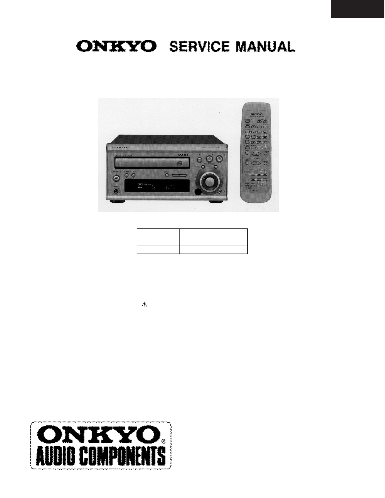
CD RECEIVER
MODEL CR-305X
CR-305X
Ref.NO.3654
082000
UDD,UDT
UPP
UGT,UGR
SAFETY-RELATED COMPONENT WARNING!!
COMPONENTS IDENTIFIED BY MARK ON THE
SCHEMATIC DIAGRAM AND IN THE PARTS LIST
ARE CRITICAL FOR RISK OF FIRE AND ELECTRIC SHOCK. REPLACE THESE COMPONENTS
WITH ONKYO PARTS WHOSE PARTS NUMBERS
APPEAR AS SHOWN IN THIS MANUAL.
MAKE LEAKAGE-CURRENT OR RESISTANCE
MEASUREMENTS TO DETERMINE THAT EXPOSED PARTS ARE ACCEPTABLY INSULATED FORM
THE SUPPLY CIRCUIT BEFORE RETURNING THE
APPLIANCE TO THE CUSTOMER.
Silver models
120 V AC,60 Hz
230 V AC,50 Hz
220 - 230 V AC,50/60Hz
TABLE OF CONTENTS
Specifications ----------------------------------------------------------Caution on replacement of optical pickup --------------------------
Protection of eyes from laser bam during servicing ---------------
Service procedures -----------------------------------------------------
Front panel view ------------------------------------------------------
Rear panel view -------------------------------------------------------
Remote controller ----------------------------------------------------
Microprocessor connection diagram --------------------------------
Microprocessor terminal descriptions ------------------------------
IC Block diagram and descriptions ---------------------------------
CD Mechanism exploded view --------------------------------------
Replacement of optical pickup ---------------------------------------
Chassis exploded view parts list -------------------------------------
Chassis exploded view -----------------------------------------------
Block diagram ---------------------------------------------------------
Wiring view ------------------------------------------------------------
Printed circuit board view parts list --------------------------------7
Schematic diagram (Amplifier section) -----------------------------
Printed circuit board view 1-------------------------------------------
Schematic diagram (CD & Microprocessor section) -------------
Printed circuit board view 2-------------------------------------------
Printed circuit board view 3-------------------------------------------
CD Adjustment procedures ------------------------------------------
Clock adjustment procedures ----------------------------------------
Assembling of pad ---------------------------------------------------
packing view ---------------------------------------------------------
2
2
3
4
5
6
7
8
9
10
19
21
22
23
25
26
27
29
31
33
35
37
39
40
41
42
Page 2

CR-305X
SPECIFICATIONS
AMPLIFIER
Power Output:
Dynamic Power: 2 x 24 watts at 4 ohms
Total Harmonic Distortion: 0.2 % at 10 watts output
IM Distortion: 0.2 % at 10 watts output
Damping Factor: 25 at 8 ohms
Sensitivity and Impedance: TAPE/CDR/MD IN : 150 mV, 50 kohms
Frequency Response: 10 to 50,000 Hz : +0 / –3 dB
Acoustic Presence: 1 40 Hz +6.0 dB
Single–to–Noise Ratio: 100 dB (IHF A)
Muting –55 dB
CD PLAYER
Signal Readout System: Optical non–contact
Reading Rotation: About 500 – 200 r.p.m.
Linear Velocity: 1.2 – 1.4 m / s
Error Correction System: Cross Interleave Reed Solomon code
D / A Converter: 1 bit
Digital Filter: 352.8 kHz 8 times over sampling
Number of Channels: 2 (stereo)
Frequency Response: 5 Hz – 20 kHz
2 x 20 watts at 4 ohms 1 kHz DIN
2 x 17 watts at 6 ohms 1 kHz DIN
2 x 15 watts at 8 ohms 1 kHz DIN
2 x 20 watts min, RMS at 4 ohms 1 kHz
no more than 1 % THD (FTC rating)
2 x 25 watts at 4 ohms EIAJ
2 x 18 watts at 8 ohms
2 80 Hz +7.5 dB
3 40 Hz +10 dB
80 Hz +8.0 dB
4 40 Hz +10 dB
80 Hz +8.0 dB
10 kHz +4.5 dB
(constant linear velocity)
TUNER
Tuning range
FM: 87.9 to 107.9 MHz (200 kHz steps)
(U.S. & Canadian models)
87.5 to 108.00 MHz (50 kHz steps)
(Other area models)
Usable sensitivity
FM: Mono 11.2 dBf,
1.0 µV (75 ohms IHF)
0.9 µV (75 ohms DIN)
Stereo 17.2 dBf,
2.0 µV (75 ohms IHF)
23.0 µV (75 ohms DIN)
50 dB Quieting sensitivity
FM: Mono 17.2 dBf, 2.0 µV (75 ohms)
Stereo 37.2 dBf, 20.0 µV (75 ohms)
Capture ratio
FM: 2.0 dB
Image rejection ratio
FM: 40 dB (U.S. & Canadian models)
85 dB (Other area models)
IF rejection ratio
FM: 90 dB
Signal to noise ratio
FM: Mono 73 dB, IHF
Stereo 67 dB, IHF
Selectivity
FM: 50 dB DIN
(±300 kHz at 40 kHz Devi.)
AM Suppression Ratio: 50 dB
Harmonic distortion
FM: Mono 0.2%
Stereo 0.3%
Frequency response
FM: 30 to 15,000 Hz (±1.5 dB)
Stereo separation
FM: 35 dB at 1,000 Hz
25 dB at 100 to 10,000 Hz
Stereo threshold
FM: 17.2 dBf, 2.0 µV (75 ohms)
AM: 530 to 1710 kHz (10 kHz steps)
(U.S. & Canadian models)
522 to 1611 kHz (9 kHz steps)
(Other area models)
AM: 30 µV
AM: 40 dB
AM: 40 dB
AM: 40 dB
AM: 0.7 %
GENERAL
Power Supply:
Power Consumption: 60 W (U.S. & Canadian models)
Dimensions:
W
eight: 4.0 kg (8.8 lbs)
Specifications and features are subject to change without notice
Power supply and voltage vary depending on the area in which the unit is
AC 120 V, 60 Hz (U.S. & Canadian models)
(Some Asian models)
AC 230 V, 50 Hz (European models)
AC 220-230 V, 50/60 Hz (Other area models)
(Some Asian models)
55 W (Other area models)
205 W x 103 H x 362 D mm
(8-1/6" x 4-1/16" x 14-1/4")
purchased.
CAUTION ON REPLACEMENT OF OPTICAL PICKUP
The laser diode in the optical pickup block is so sensitive to
static electricity, surge current and etc., that the components
are liable to be broken down or its reliability remarkably
deteriorated.
PRECAUTIONS
1.Ground for the work-desk.
Place a conductive sheet such as a sheet of copper
(with impedance lower than 10Mohm) on the workdesk and place the set on the conductive sheet so that
the chassis can be grounded.
2.Grounding for the test equipments and tools.
Test equipments and toolings should be grounded in
order that their ground level is the same the ground of
the power source.
㧙
During repair,carefully take the following precautions.
(The following precautions are included in the service
parts.)
3. Grounding for the human body.
Be sure to put on a wrist-strap for grounding whose
other end is grounded.
Be particularly careful when the workers wear
synthetic fiber clothes, or air is dry.
4. Select a soldering iron that permits no leakage and
have the tip of the iron well-grounded.
5. Do not check the laser diode terminals with the
probe of a circuit tester or oscilloscope.
㧙
1
.
Page 3
CR-305X
PROTECTION OF EYES FROM LASER BEAM DURING SERVICING
This set employs a laser. Therefore, be sure to follow carefully
the instructions below when servicing.
WARNING!!
SERVICE WARNING : DO NOT APPROACH THE
LASER EXIT WITH THE EYE TOO CLOSELY.
IN CASE IT IS NECESSARY TO CONFIRM LASER
BEAM EMISSION, BE SURE TO OBSERVE FROM
A DISTANCE OF MORE THAN 30cm FROM THE
SURFACE OF THE OBJECTIVE LENS ON THE
OPTICAL PICK-UP BLOCK.
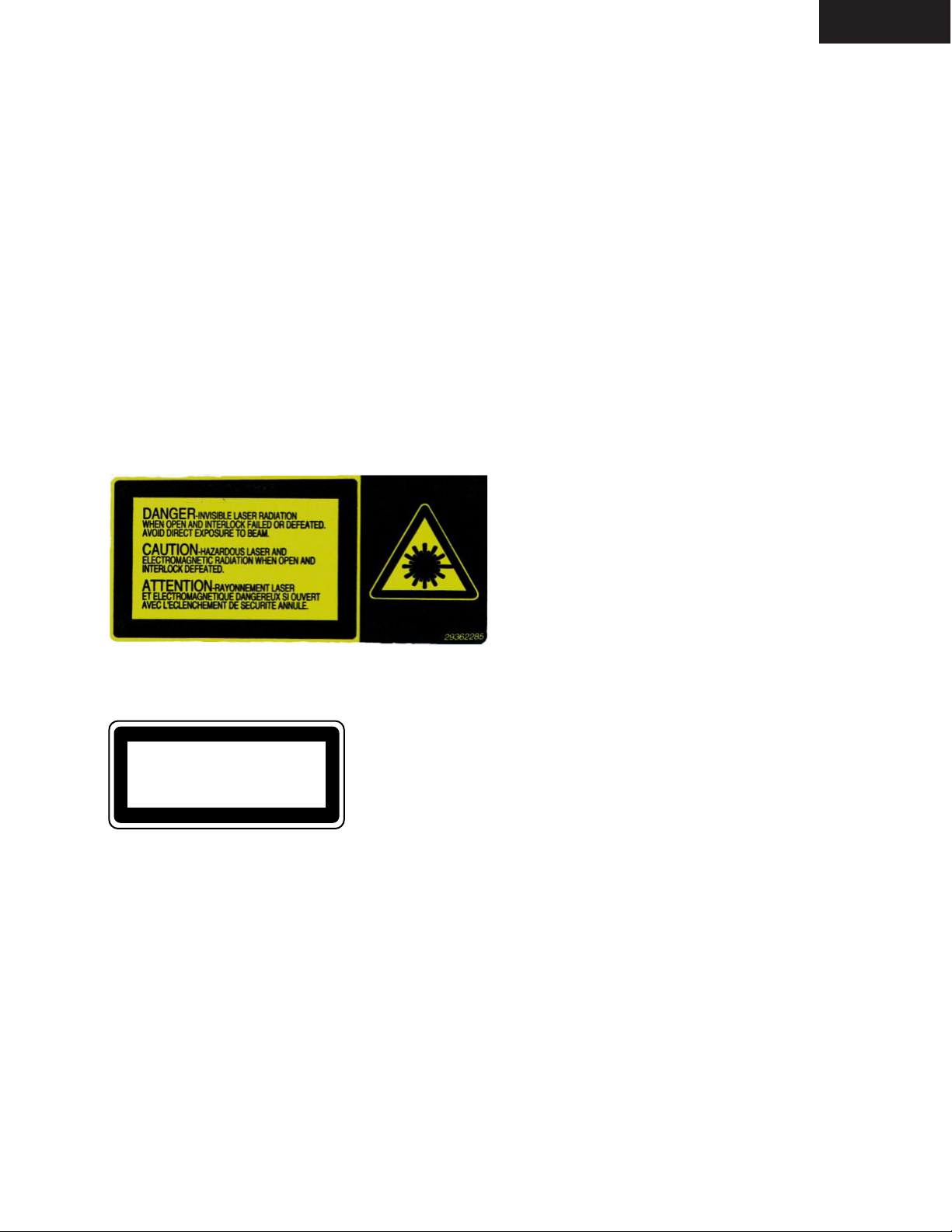
LASER WARNING LABEL
The label shown below are affixed.
1. Warning label
Laser Diode Properties
Material: GaAS/GaALAs
Wavelength: 780nm
Laser output: max. 0.5mW*
Emission Duration: continuous
*This output is the value measured at a distance about 1.8mm
from the objective lens surface on the Optical Pick-up Block.
1. Class 1 label
"CLASS 1 LASER
PRODUCT"
LUOKAN 1
LASERLAITE
KLASS 1
LASER APPARAT
㧙
㧙
3
Page 4
CR-305X
SERVICE PROCEDURE
1. Replacing the fuses
This symbol located near the fuse indicates that the
fuse used is show operating type, For continued protection against
fire hazard, replace with same type fuse , For fuse rating, refer to
the marking adjest to the symbol.
Ce symbole indique que le fusible utilise est e lent.
Pour une protection permanente, n'utiliser que des fusibles de meme
type. Ce demier est indique la qu le present symbol est apposre.
REF.NO.
F901
PART NO.
252157
252083
NOTE : <D, DT> : 120 V model only
<P,GR, GT> : 230 V model only
DESCRIPTION
1.25A-UL/T-237, Fuse <D, DT>
0.4A-SE-EAW, FUSE <P,GR, GT>
2. To initialize the unit
1. Press and the hold down the MEMORY button , then press the
After "all lighting " is displayed
2. Press the standby/on button.
After " CLEAR " is displayed, the preset memory and each mode
stored in the memory, are initialized and will return to the
factory settings.
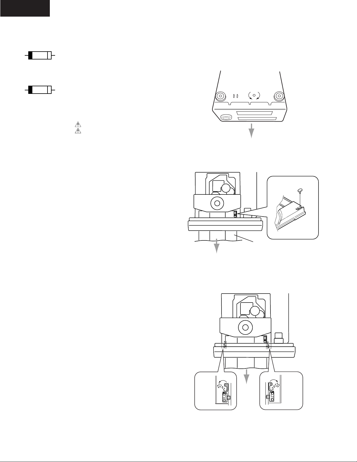
5. Removement of tray
1.Remove the top cover
2.Turn the locked screw to the clockwise to release the lock of gear.
(Refer to fig-1)
Fig-1
Bottom side
Lock
Unlock
Front
3.Pull out the tray.
4.Remove the stopper. (Refer to fig-2)
Fig-2
Stopper
3. Safety-check out
(Only U.S.A. model)
After correcting the original service problem perform the
follwing safety check before releasing the set to the customer
Connect the insulating-resistance tester between the plug of
power supply cord and terminal GND on the back panel.
Specifications: More than 10Mohm at 500V
4. Memory Preservation
This unit does not require memory preservation batteries. A built-in
memory power back-up system preserves the contents of the
memory during power failures and even when the unit is un-plugged.
The unit must be plugged in order to charge the back-up
system.
The memory preservation period after the unit has been unplugged
varies depending on climate and placement of the unit. On the
average, memory contents are protected over a period of a few
weeks after the last time the unit has been unplugged. This pe-riod
is shorter when the unit is exposed to a highly humid cli-mate.
5. Changing the AM band step
With the exception of the worldwide models, a tuning step selector
switch is not provided. When you change the band step, change
the parts as shown below.
To 10kHz To 9kHz
R705 3.3k 10k
R706 5.6k open
Tray
Front
5.Press teh tray stopper to the arrow mark direction and remove
the tray ass'y. (Refer to fig-3)
Fig-3
Tray
stopper
Front
Tray
stopper
㧙
㧙
4
Page 5
CR-305X
DETECTOR SWITCH
CD TRAY OPEN/CLOSE
Q703
Q184-Q186
SYSTEM RESET
CD MUTNG SWITCH
26 SENS2
Q101
CXA1992BR
SERVO AMP
RF SIGNAL PROCESSING
23 XRST
KEY SWITCH
S762 S761 S760 S759 S758 S757
VOLUME
M
Q704
MOTOR DRIVE IC
SENS 6
SQSO 5
SQCK 4
Q301
CXD2589Q
CD DIGITAL
SIGNAL PROCESSOR
FR FF PLAY STOP OPEN MEMORY
TA7291S
DATA 7
XLAT 8
57 SCOR
79 XRST
STBY
AUTO
/MONO
DISPLAY
SD
STEREO
INPUT<
INPUT>
S756 S755 S754 S753 S752 S751
AP
(FM/AM BAND)
INITIALIZING
24
AREA
23
22
21
20
AVSS
19
SD
18
17
16
SQSO
15
SENS
14
SQCK
13
12
11
10
XLT
9
+5V
8
VDD
7
10G
6
9G
5
8G
4
GRID
IG - 10G
7G
3
6G
2
5G
1
4G
CLOK 9
U10
TUNER UNIT
K1
K0
P17
+5V
AVDD
P16
PLL
POWER
AVREF
P15
P11-P17
SEGMENT
SIGNAL
252627282930313233343536373839
IN/OUT
SIGNAL
VOLUP
VOLDOWN
STEREO
RESET
DSPMUT
SENS20
CDDATA
CDCLK
3G2G1G
807978777675747372717069686766
Q401
TC9273N-007
RDATA
DETECTOR
XT2
VSS
X1
INPUT SELECTOR
C703
( CLOCK ADJUST)
X2
RCLK
14 CK
RDATA
15 DATA
RCLK
FAILURE
POFF
Q701
MICROPROCESSOR
MPD78045FGF-119-3B9
P14
P13
P12
P11
VLOAD
P10P9P8P7P6
-VP
SEGMENT
TP-01
FREQCAL
P1 - P10
16 ST
( CLOCK ADJUST )
40
FCE
PLLCE
65
Q402
SELECTOR IC
ACOUSTIC PRESENCE
13 ST
15 CK
16 DATA
POWERAMP
41
RDSDATA
42
RDSSIG
43
SCOR
44
RDSCLK
45
SYSIN
46
REMIN
47
IC
48
SYSOUT
49
TUMUT
50
ANGMUT
51
VDD
52
POWERCD
53
LED1
54
XRST
55
CDAUTOADJ
56
OPEN
57
CLOSE
58
LED2
59
P1
60
P2
61
P3
62
P4
63
P5
64
Q702
+5V
LED DRIVE
Q601,Q602
POWER AMP SWITCH
Q180
BU1923
RDS DECODER
2 RDATA
16 RCLK
1 QUAL
+5V
Q704
TA7291S
MOTOR DRIVE IC
Q904
POWER
RELAY DRIVE
U751
REMOTE
INITIALIZING
(CD AUTO ADUST ON/OFF)
Q702
BUFFER
SENSOR
Q110,Q111
CD POWER SWTCH
RI
Q181-Q183
TUNER MUTE SWITCH
Q405,Q406
INPUT MUTE SWITCH
Q751
FL TUBE
10-BT-167GK
D782
ACOUSTIC
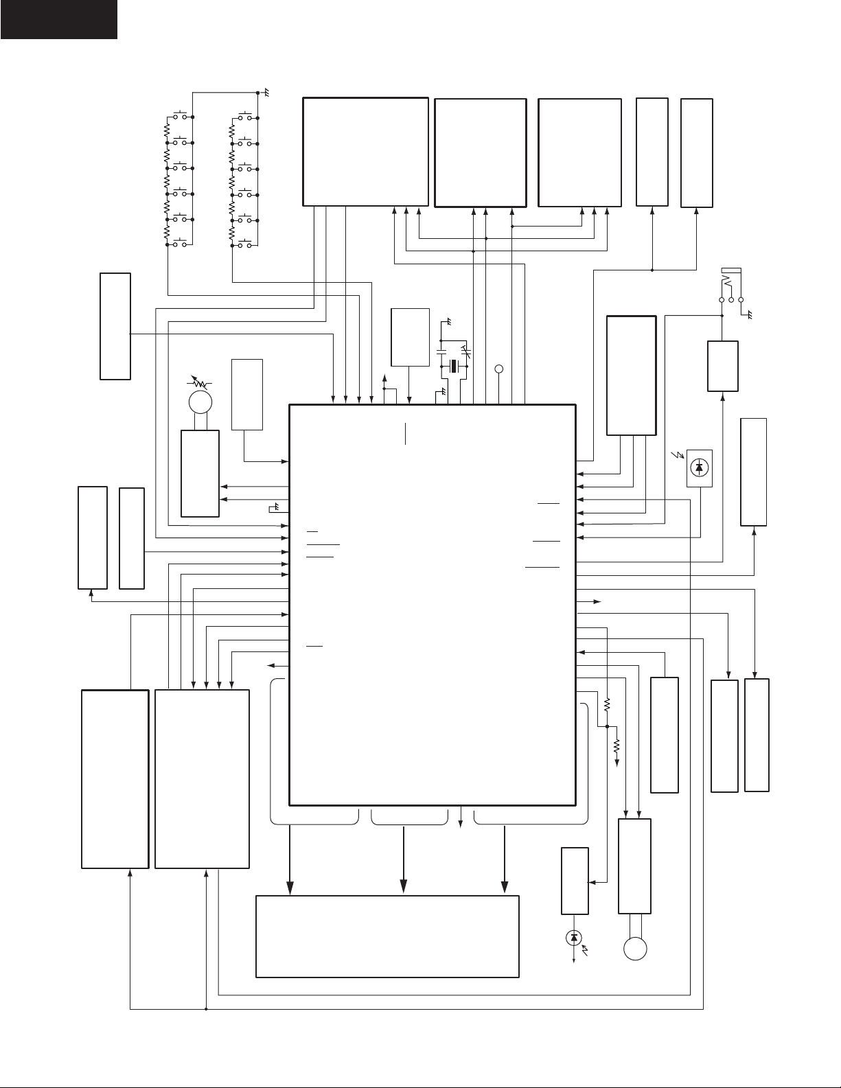
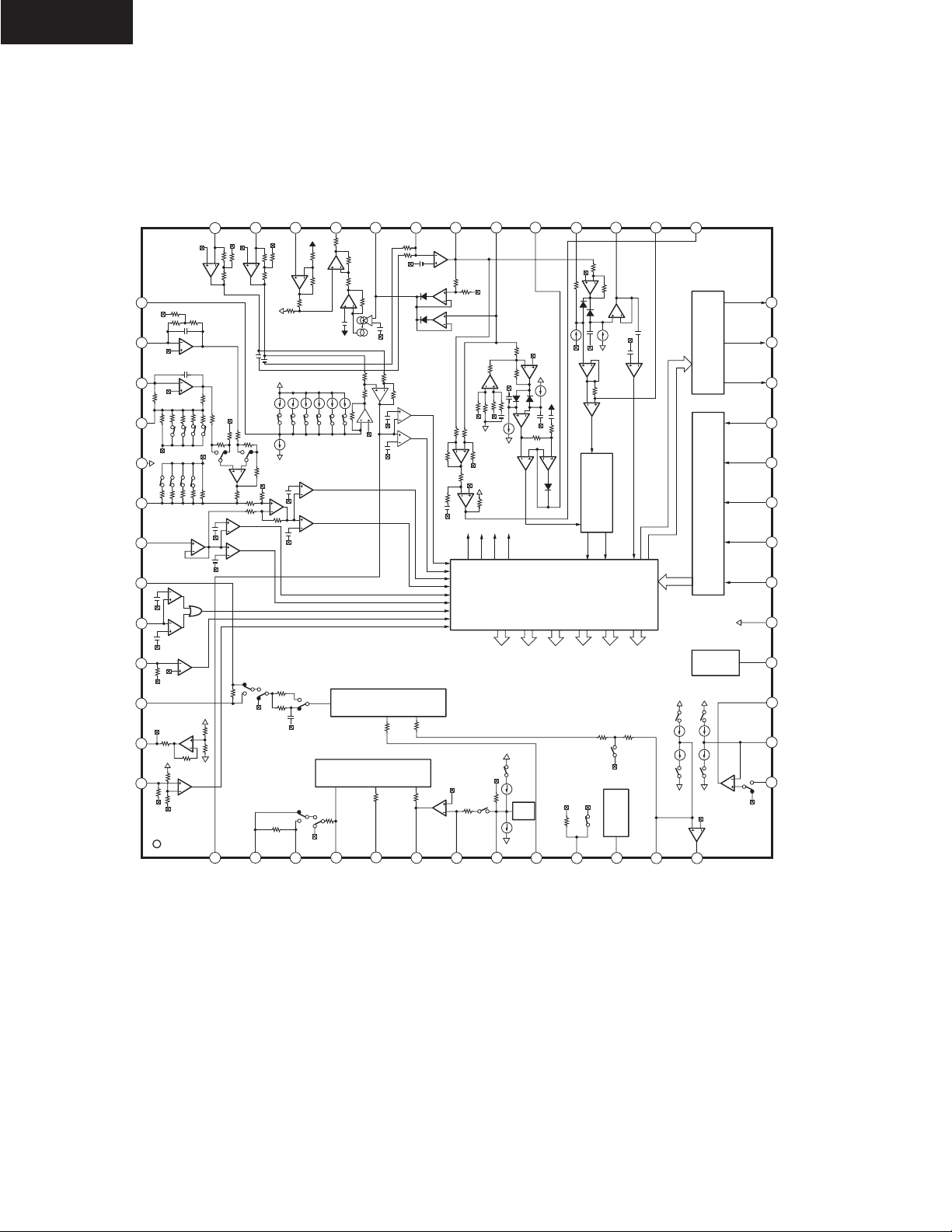
MICROPROCESSOR CONNECTION DIAGRAM
㧙
㧙
8
PRESENCE
+5V
M
CD TRAY
OPEN/CLOSE
Page 6
Description
CR-305X
P11)
㨪
Output pin for power supply control of power amplifier
Data input pin from RDS decoder IC.
Signal input pin from RDS decoder IC.
Sub code frame detection input pin from signal processing IC(CXD2589Q).
Clock input pin from RDS decoder IC.
System code input pin.
Signal input pin for remote controller.
Internal connection pin. Not used.
System code output pin.
Muting control signal output pin for tuner section.
Muting control signal output pin for amplifier section.
Power supply pin.
Output pin for power supply control of CD section.
Acoustic presence indicator (red) control output pin.
Reset signal output pin of signal processing IC and servo IC.
Set pin of self adjustment ON/OFF of CD
CD tray open control output pin.
CD tray close control output pin.
Acoustic presence indicator (green) control output pin.
I
I
I
I
I
I
O
I/O
Function
POWER AMP
RDSDATA
RDSSIG
SCOR
RDSSCK
414243444546474849505152535455565758596061626364656667686970717273747576777879
NO.
I
SYSIN
REMINICSYSOUT
OOOIOOOIOOO
TUMUT
ANGMUT
VDD
POWERCD
LED1
XRST
CDAUTOADJ
OPEN
CLOSE
LED2P1P2P3P4P5P6P7P8P9P10
Segment output pins. (P1
Power supply pin for FL tube.
P11
VLOAD
P17)
㨪
Segment output pins. (P12
P12
P13
P14
P15
P16
3G)
㨪
Grid output pins. (1G
P171G2G
3G
80
Description
10G)
㨪
Grid output pins. (4G
OOOOOOOIOOOIO
I/O
Function4G5G6G7G8G9G
MICROPROCESSOR TERMINAL DESCRIPTION (Q701 : MPD78042GF-3B9)
123456789
NO.
Power supply pin.
Command output pin to transfer the clock signal to signal processing IC(CXD2589Q).
Command output pin to transfer the latch signal to signal processing IC(CXD2589Q).
Command output pin to transfer the data signal to signal processing IC(CXD2589Q).
Sense signal input pin from servo IC(CXA1992)
Digital mute output pin to signal processing IC(CXD2589Q).
Subcode reading clock output pin to signal processing IC(CXD2589Q).
Sense signal input pin from signal processing IC(CXD2589Q).
Subcode data input pin from signal processing IC(CXD2589Q).
System reset input pin.
FM stereo broadcast detection input pin.
Broadcast detection input pin.
Ground pin for A/D converter.
Volume control output pin.
Volume control output pin.
Not used.
Initialization input pin for destination switch.
Input pin for CD tray open/close detection switches.
Signal level input pin for automatic memory.
Operation key connection pin.
Operation key connection pin.
I
I
10G
SENS
III
SQSO
RESET
O
VDD
CDCLK
XLT
CDDATA
SENS20
DSPMUT
SQCK
10111213141516171819202122232425262728293031323334353637383940
I
STEREOSDAVSS
㧙
9
O
VOLDOWN
㧙
-
O
VOLUP
I
I
AREA
IN/OUT
I
I
I
SIGNALK1KO
Power supply pin for A/D converter.
I
AVDD
Reference voltage input pin for A/D converter.
I
AVREF
Power failure input pin.
Sub clock connection pin. Not used.
Gound pin.
Master clock connection pin.
Master clock connection pin.
Serial clock output pin to PLL and function switch ICs (TC9273,TC9162).
Serial data output pin to PLL and function switch ICs(TC9273,TC9162).
Frequency output terminal for clock adjustment
Serial latch output pin to function switch ICs(TC9273,TC9162).
IOI
POFF
XT2
VSSX1X2
I
I
OOOOO
RCLK
RDATA
FREQCAL
FCE
Serial latch output pin to PLL IC.
PLLCE
Page 7
CR-305X
IC BLOCK DIAGRAM AND DESCRIPTIONS
Q101:CXA1992BR (RF Signal Processing Servo Amplifier)
Block Diagram
FE-BIAS
V
TEO
LPFI
TEI
ATSC
TZC
TDFCT
VC
FZC
O
-
RF
M
-
FE
LDON
VEE
LEVEL S
VCC
LPCL
FS2
323334353637
LPC
DFCTO IFB1-6
FS1
8
I
-
RF
CP
31
VCC
VEE
VEE
MIRR
TGFL
IIL DATA REGISTER
INPUT SHIFT REGISTER
ADDRESS DECODER
SENS SELECTOR
OUTPUT DECODER
FS1-4 TG1-2
BAL1-4
TOG1-4
VCC
Charge
up
VEE
9
TGU
SRCH
30
TG2
10
CB
MIRR
TG2
V
CC
DFCT
IIL
↓
TTL
TN1-7 PS1-4
TM3
FSET
11
CC1
DFCT1
FSET
FOK
CC2
2829
27
26
SENS2
IIL
↓
TTL
TTL
↓
IIL
CC1
ISET
VCC
VCC
TM4
TM6
TM3
TM5
VEE
VEE
12
13
O
M
-
TA
TA
25
SENS1
24
C.OUT
23
XRST
22
DATA
XLT
21
CLK
20
LOCK
19
VCC
TM2
CC
V
18
ISET
17
16
SL-O
15
SL-M
14
SL-P
M
-
RFTC
RF SUMMING AMP
FO.BIAS
WINDOW COMP.
RF
FOK
FOH
FOL
TGH
TGL
BALH
BALL
ATSC
TZC
FZC
PD
VEE
APC
LASER POWER CONTROL
IFB5
IFB3
IFB4
TRK.GAIN
WINDOW COMP
LD
VEE
FE AMP
IFB6
PD1
PD2
3839
PD1 IV
PD2 IV
AMP
AMP
40
41
F
42
E
EI
43
EE
44
F IV AMP
E IV AMP
BAL1
BAL2
BAL3
VEE
TOG1
BAL4
TOG2
TOG3
TOG4
TGFL
VCC
VCC
IFB2
IFB1
VEE
45
E-F BALANCE
46
WINDOW COMP.
47
48
ATSC
WINDOW
COMP.
TZC COMP.
49
50
VCC
DFCT
TM1
TG1
TRACKING
PHASE COMPENSATION
51
VCC
VEE
52
FZC COMP.
12
FEI
FEO
FOCUS
PHASE COMPENSATION
DFCT
FS4
45
3
FDFCT
FGD
FLB
6
7
O
-
FE
㧙
㧙
10
Page 8
Terminal description
CR-305X
Pin
Symbol
No.
1 FEO O
2 FEI Focus error input. I
34FDFCT
FGD I
5 FLB
6 FE_O
7
FE_M
8 SRCH
9
TGU
10
TG2
11
FSET
12 TA_M I Tracking amplifier inverted input.
TA_O
13
14
SL_P
15
SL_M
16 SL_O O Sled drive output.
17 ISET I Connect an external capacitance to set the current
18
VCC
19 LOCK I
20 CLK
XLT
21
22 DATA
XRST I Reset input; resets at Low. (no pull-up resistance)
23
24 C. OUT
SENS1
25
I/O
Focus error amplifier output.
Connected internally to the window comparator input
for bias adjustment.
I
Capacitor connection pin for defect time constant.
Ground this pin through a capacitor for cutting the
focus servo high-frequency gain.
External time constant setting pin for boosting the
I
focus servo low-frequency.
O
Focus drive output.
I Focus amplifier inverted input.
I
External time constant setting pin for generating
focus search waveform.
I External time constant setting pin for switching track-
ing high-frequency gain.
External time constant setting pin for switching track-
I
ing high-frequency gain.
Peak frequency setting pin for focus and tracking
I
phase compensation amplifier.
O Tracking drive output.
I Sled amplifier non-inverted input.
I Sled amplifier inverted input.
which determines the Focus search, Track jump, and
Sled kick heights.
I Positive power supply.
The sled overrun prevention circuit operates when
this pin is Low. (no pull-up resistance)
I
Serial data transfer clock input from CPU.
(no pull-up resistance)
I
Latch input from CPU. (no pull-up resistance)
Serial data input from CPU. (no pull-up resistance)
I
O
Track number count signal output.
O
Outputs FZC, DFCT1, TZC, BALH, TGH, FOH,
ATSC, and others according to the command from
CPU.
Description
Pin
Symbol
No.
26 SENS2 O
27
FOK
28
CC2 I
CC1
29
30 CB
31 CP
32
RF_I I
33 RF_O
34 RF_M
35 RFTC
LD O APC amplifier output.
36
PD I APC amplifier input.
37
PD1
38
39
PD2
40
FE_BIAS
41
F
42IE
43 EI
44
VEE
45 TEO O
46 LPFI I Comparator input for balance adjustment.
47
TEI
ATSC
48
49
TZC
50
TDFCT
51
VC
52 FZC
I/O
Outputs DFCT2, MIRR, BALL, TGL, FOL, and
others according to the command from the CPU.
O Focus OK comparator output.
Input for the defect bottom hold output with capacitance coupled.
O Defect bottom hold output. Connected internally to
the interruption comparator input.
Connection pin for defect bottom hold capacitor.
I
Connection pin for MIRR hold capacitor.
I
MIRR comparator non-inverted input.
Input for the RF summing amplifier output with capa-
citance coupled.
RF sunning amplifier output. Eyepattern check point.
O
RF summing amplifier inverted input.
I
The RF amplifier gain is determined by the resistance
connected
between this pin and RFO pin.
I
External time constant setting pin during RF level
control.
I
RF I-V amplifier inverted input. Connect these pins
to the photo diode A + C and B + D pins.
I
I
Bias adjustment of focus error amplifier.
Leave this pin open for automatic adjustment.
I
F I-V and E I-V amplifier inverted input.
Connect these pins to photo diodes F and E.
—
I-V amplifier E gain adjustment.
(When not using automatic balance adjustment)
—
Negative power supply.
Tracking error amplifier output. E-F signal is output.
(Input from TEO through LPF)
Tracking error input.
I
Window comparator input for ATSC detection.
I
I
Tracking zero-cross comparator input.
I
Capacitor connection pin for defect time constant.
O (VCC + VEE)/2 direct voltage output.
I
Focus zero-cross comparator input.
Description
㧙
㧙
11
Page 9

CR-305X
Q301:CXD2589Q (CD Digital Signal Processor)
Bloch Diagram
XTSL
VPCO
VCKI
V16M
VCTL
XUGF
GFS
EMPH
EFM
WFCK
56
54
C4M
RF
ASYI
ASYO
BIAS
XPCK
FILO
FILI
PCO
CLTV
52
52
35
35
37
37
38
38
36
36
48
48
30
30
31
31
29
29
33
33
51
51 25 26 27 28 47 49 54 56 50 39 41 43 55 40 42 44 62
25
Clock
28
26
27
49
47
OSC
Generator
demodurator
Asymmetry
Corrector
Digital
PLL
Sub Code
Processor
Error
Corrector
16K
RAM
C2PO
LRCK
39
41
50
D/A
Interface
Digital
OUT
PCMD
BCK
EMPHI
LRCKI
40
55
Serial-In
Interface
Over Sampling
Digital Filter
PWM
PCMDI
BCKI
SYSM
424344
62
Timing
Logic
3rd-Order
Noise Shaper
PWM
24
24
23
23
79
79
3
3
2
2
70
70
71
71
TES1
TEST
XRST
RMUT
LMUT
XTAI
XTAO
FOK
SEIN
CNIN
18
18
Servo
10
10
11
11
Auto
Sequencer
12 13 14 6 7 8 9 15 16 17 57 58 59 5 4 21 22 53 74 75 76 67 66 65
14
13
12
DATO
CLKO
XLTO
CPU
Interface
65
7
SENS
15 16 17
XLAT
DATA
CLOK
SPOA
XLON
SPOB
57
58
SCOR
9
8
59
EXCK
SBSO
4
SQCK
SQSO
Digital
CLV
21
MDP
22
PWMI
53
DOUT
74
LOUT2
75
76
AIN2
AOUT2
67
66
AIN1
LOUT1
65
AOUT1
㧙
㧙
12
Page 10

Terminal description
Pin
No.
10
11
12
13
14
15
16
17
18
19
20
21
22
23
24
25
26
27
28
29
30
31
32
33
34
35
36
37
38
39
40
41
42
1
2
3
4
5
6
7
8
9
Symbol
VSS
LMUT
RMUT
SQCK
SQSO
SENS
DATA
XLAT
CLOK
SEIN
CNIN
DATO
XLTO
CLKO
SPOA
SPOB
XLON
FOK
VDD
VSS
MDP
PWMI
TEST
TES1
VPCO
VCKI
V16M
VCTL
PCO
FILO
FILI
AVSS
CLTV
AVDD
RF
BIAS
ASYI
ASYO
LRCK
LRCKI
PCMD
PCMDI
I/O
GND
—
Left-channel zero detection flag.
O
Right-channel zero detection flag.
O
SQSO readout clock input.
I
Sub Q 80-bit serial output.
O
SENS output to CPU.
O
Serial data input from CPU.
I
Latch input from CPU. Serial data is latched at the
I
falling edge.
Serial data transfer clock input from CPU.
I
SENS input from SSP.
I
Track jump count signal input.
I
Serial data output to SSP.
O
Serial data latch output to SSP. Latched at the falling
O
edge.
Serial data transfer clock output to SSP.
O
Microcomputer extended interface (input A).
I
Microcomputer extended interface (input B).
I
Microcomputer extended interface (output).
O
Focus OK input.
I
Used for SENS output and the servo auto sequencer.
Power supply (+5V).
—
GND
—
Spindle motor servo control.
O
Spindle motor external control input.
I
TEST pin; normally GND.
I
TEST pin; normally GND.
I
Charge pump output for the wide-band EFM PLL.
O
VCO2 oscillation input for the wide-band EFM PLL.
I
VCO2 oscillation output for the wide-band EFM
O
PLL.
VCO2 control voltage input for the wide-band EFM
I
PLL.
Master PLL charge pump output.
O
Master PLL (slave = digital PLL) filter output.
O
Master PLL filter input.
I
Analog GND.
—
Master VCO control voltage input.
I
Analog power supply (+5V).
—
EFM signal input.
I
Constant current input of the asymmetry circuit.
I
Asymmetry comparator voltage input.
I
EFM full-swing output (low = VSS, high = VDD).
O
D/A interface. LR clock output f = Fs.
O
LR clock input.
I
D/A interface. Serial data output (two's complement,
O
MSB first).
D/A interface. Serial data input (two's complement,
I
MSB first).
Description
Pin
No.
43
44
45
46
47
48
49
50
51
52
53
54
55
56
57
58
59
60
61
62
63
64
65
66
67
68
69
70
71
72
73
74
75
76
77
78
79
80
Symbol
BCK
BCKI
VSS
VDD
XUGF
XPCK
GFS
C2PO
XTSL
C4M
DOUT
EMPH
EMPHI
WFCK
SCOR
SBSO
EXCK
VSS
VDD
SYSM
AVSS
AVDD
AOUT1
AIN1
LOUT1
AVSS
XVDD
XTAI
XTAO
XVSS
AVSS
LOUT2
AIN2
AOUT2
AVDD
AVSS
XRST
VDD
I/O
D/A interface. Bit clock output.
O
D/A interface. Bit clock input.
I
GND
—
Power supply (+5V).
—
XUGF output. Switched to MNT1 or RFCK output
O
by a command.
XPLCK output. Switched to MNT0 output by a com-
O
mand.
GFS output. Switched to MNT3 or XRAOF output
O
by a command.
C2PO output. Switched to GTOP output by a com-
O
mand.
Crystal selector input. Low: 16.9344MHz;
I
high: 33.8688MHz.
4.2336MHz output. 1/4 frequency-divided VCKI out-
O
put in CAV-W mode.
Digital Out output.
O
Outputs a high signal when the playback disc has
O
emphasis, and a low signal when there is no emphasis.
Inputs a high signal when de-emphasis is on, and a
I
low signal when de-emphasis is off.
WFCK output.
O
Outputs a high signal when either subcode sync S0
O
or S1 is detected.
Sub P to W serial output.
O
SBSO readout clock input.
I
GND
—
Power supply (+5V).
—
Mute input. Active when high.
I
Analog GND.
—
Analog power supply (+5V).
—
Left-channel analog output.
O
Left-channel operational amplifier input.
I
Left-channel LINE output.
O
Analog GND.
—
Power supply for master clock.
Crystal oscillation circuit input. Input the external
I
master clock via this pin.
Crystal oscillation circuit output.
O
GND for master clock.
Analog GND.
—
Right-channel LINE output.
O
Right-channel operational amplifier input.
I
Right-channel analog output.
O
Analog power supply (+5V).
—
Analog GND.
—
System reset. Reset when low.
I
Power supply (+5V).
—
Description
CR-305X
Notes)
• PCMD is an MSB first, two's complement output.
• GTOP is used to monitor the frame sync protection status. (High: sync protection window open.)
• XUGF is the frame sync obtained from the EFM signal, and a negative pulse. It is the signal before
sync protection.
• XPLCK is the inverse of the EFM PLL clock. The PLL is designed so that the falling edge of XPLCK
and the EFM signal transition point coincide.
• GFS goes high when the frame sync and the insertion protection timing match.
• RFCK is derived with the crystal accuracy. This signal has a cycle of 136µs (during normal speed).
• C2PO represents the data error status.
• XRAOF is generated when the 16K RAM exceeds the ±4F jitter margin.
㧙
㧙
13
Page 11

CR-305X
Q401:TC9273N-007 (Analog function switch)
VSS
VDD
128
2
S1
3
S2
4
S3
5
S4
6
S5
7
S6
8
S7
9
OUT
10
S8
11
S9
12
OUT
GND CK DATA STB
Q402:TC9162AF Analog function switch
2
S1
10BITS LATCH CIRCUIT
LEVEL SHIFT AND
SHIFT REGISTER
13 14 15 16
VSS
GND
1
14
10BITS LATCH CIRCUIT
VDD
28
27
26
25
24
23
22
21
20
19
18
17
S1
S2
S3
S4
S5
S6
S7
OUT
S8
S9
OUT
27
S1
S2
S3
COM1
S4
S5
S6
COM2
S7
S8
COM3
ST
11
12
13
10
S2
16
26
25
24
23
22
21
20
19
18
17
15
S3
COM1
S4
S5
S6
COM2
S7
S8
COM3
DATA
CK
3
4
5
6
7
8
9
LATCH CIRCUIT
LEVEL SHIFTER
SHIFT REGISTER
㧙
㧙
14
LATCH CIRCUIT
LEVEL SHIFTER
Page 12

CR-305X
CMP
VSS3
(8)
(7)
ǡ
100 k
(4)
MUX
Comparator
8ch Switched
capacitor filter
+
anti-aliasing
ǡ
100 k
ǡ
(3)
120 k
filter
VREF
RCLK
(16)
(5)
QUAL
(1)
Analog
Power supply
(6)
VDD1
RDATA
(2)
PLL
PLL
VSS1
decoder
Differential
decoder
Bi-phase
1187.5 Hz
57 kHz
RDS/ARI
Digital
power supply
(12)
VDD2
circuit
Measurement
clock
Reference
(11)
VSS2
(9)
(10)
(13) (14)
XO
X1
T2T1
㧙
16
Function
Good data : High , bad data : Low
Refer to output data trimming
1/2 VDD1
Composite signal input
4.5 V to 5.5 V
Pin name
Demodulator quality
Demodulator data
Reference voltage
Input
Analog power supply
Vref
Vss1
MUX
QUAL
Symbol
RDATA
123456789
Pin No.
VDD1
-
C-junction
Open or connected to ground
4.5 V to 5.5 V
GND
Comparator input
Test input
Digital power supply
T2
T1
Vss3
CMP
VDD2
10111213141516
Connects to 4.332 MHz oscillator
-
1187.5 Hz clock
Crystal oscillor
-
Demodulator clock
XI
XO
Vss2
(NC)
RCLK
㧙
Q180:BU1923 (RDS Decoder(
16
RES
17
CD
18
VIN3
19
VG3
20
Vo5
21
Vo6
22
GND
23
GND
24
GND
25
Vo7
26
Vo8
27
VG4
28
VIN4
29
Vref
30
Vcc
RESET
Level shift
BTL AMP
BTL AMP
Level shift
2
2
1
1
3
3
Vcc
4
4
Regulator
Level shift
BTL AMP
BTL AMP
Level shift
15
Reg IN
14
Reg OUT
13
VI2
12
VG2
11
Vo4
10
Vo3
9
GND
8
GND
7
GND
6
Vo2
5
Vo1
4
VG1
3
VIN1
2
Mute
1
Vcc
Power supply (shorted with pin 30)
1 BTL AMP 1 input
1 BTL AMP 1 output (non-inverting side)
2 BTL AMP 1 output (inverting side)
O
CC
O
IN
3 BTL AMP 2 output (inverting side)
O
4 BTL AMP 2 output (non-inverting side)
O
2 BTL AMP 2 input
IN
Reset output
Reset output delay time setting (with capacitor)
3 BTL AMP 3 input
D
IN
5 BTL AMP 3 output (non-inverting side)
O
6 BTL AMP 3 output (inverting side)
O
7 BTL AMP 4 output (inverting side)
O
8 BTL AMP 4 output (non-inverting side)
O
4 BTL AMP 4 input
IN
Reference voltage input for level shift circuit
REF
㧙
15
㧙
Power supply (shorted with pin 1)
CC
2 Mute ON/OFF control for all BTL AMP outputs
3V
4 VG1 BTLAMP 1 input (for gain control)
1V
Pin No. Pin Name Description (Function)
5V
Q102:LA6541D (4-channel ridge Driver for Compact Dizcs)
6V
7 GND GND (minimum electric potential)
8 GND GND (minimum electric potential)
9 GND GND (minimum electric potential)
11 V
12 VG2 BTL AMP 2 input (for gain control)
10 V
17 C
15 REG IN Connection for base of external transistor (PNP)
16 RES
18 V
19 VG3 BTL AMP 3 input (for gain control)
21 V
22 GND GND (minimum electric potential)
23 GND GND (minimum electric potential)
24 GND GND (minimum electric potential)
25 V
20 V
26 V
13 V
14 REG OUT Connection for collector of external transistor (PNP); 5 V supply output
27 VG4 BTL AMP 4 input (for gain control)
30 V
28 V
29 V
Page 13

b
c
k
n
j
a
m
g
r
S.BASS
MUTING
STEREO
MIN
kHz
ST
RDS
PMAM
e
p
DIRECT
MHz
d
(9G - 2G)
h
f
MIN
S.BASS
MUTING
MHz
kHz
DIRECT
T STEREO
--
-
Dp
Col
㧙
18
㧙
CR-305X
CR-305X
MONOAUTOTRACKTIMER
CD
MEMORY
REPEAT
W.DAY
W.END
RANDOM
REC
SLEEP
10G 9G 8G 7G 6G 5G 4G 3G 2G 1G
Q751 : 10BT-167GK (FL TUBE)
STOP
MODE
CW/CCW
LHL
п
OUT2
OUTPUT
H
п
OUT1
001
IN2
INPUT
010
IN1
jjjjjjjj
hhhhhhhh
10G 9G 8G 7G 6G 5G 4G 3G 2G 1G
W.END
W.DAY
P1- aaaaaaaa -
P2
P3
BRAKE
CCW/SW
L
L
1
1
CCW : Counter clockwise diection
CW : Clockwise diection
----
kkkkkkkk
MEMORY
P4
P5- bbbbbbbb -
P6- ffffffff -
P7- gggggggg -
nnnnnnnn
REPEAT
P9- cccccccc -
P10- eeeeeeee -
P11
r r r r rr r r r
RANDOM
P12
P13- pppppppp -
mmmmmmmm
REC
P8
-----
CD
SLEEP
TIMER TRACK AUTO MONO AM PM RDS S
P17
P14- dddddddd -
P15
P16
Vss
6
Vref
Vcc
8
2
REG
Q103:TA7291S (motor driver)
OUT1
7
ً
ً
OUT2
3
PROTECTOR
AY
L H
H L
Truth table
㧙
17
㧙
ً
Vcc
1Y
3A
2Y
6
7
8
ً
159
1
1A
IN1 IN2 GND
2
3Y
3
45
2A
GND
Q691:TC7WU04FU (triple inverters)
Page 14

p
p
p
CR-305X
61
59
62
54
60
63
51
tion
51 X2625-984-1 Motor chassis ass'y
52 X2625-769-1 Motor gear ass'y
53 2656-908-01 Sled shaft
54 2625-188-02 Gear A
55 7621-255-15 P2x3, Screw
56 1572-085-11 Leaf switch
57 1639-678-12 Motor PC board
58 1564-722-11 Socket
59 2627-003-02 Gear B
60 2625-191-01 Coil spring
61 2625-477-01 Center ring
62 2641-386-01 Special screw, 2*5
63 2625-625-01 Reinforcement board
Ref. No. Part No. Descri
The mechanical parts with no part number
in the exploded views are not supplied.
56
64 8848-483-05 KSS-213C, Pickup
57
tion
16 2627-234-01 Insulator
17 KSM-213CCM
Ref. No. Part No. Descri
18 2625-552-06 Main chassis
19 3319-501-51 PTPWH2.6*16, Screw
20 2625-547-01 Drive Gear
21 2625-545-04 Control cam
22 1692-667-11 Leaf switch
23 1564-721-11 Socket
24 1640-523-11 Loading motor ass'y
25 X2625-117-1 Loading motor
26 2625-274-02 Middle gear
27 2625-536-02 Loading pulley
28 3653-387-00 LM belt
29 B2.6*2.5, Screw
㧙
20
㧙
55
53
64
pickup drive unit
CD MECHANISM EXPLODEE VIEW(2)
6
16
6
11
6
17
16
131415
121415
16
121415
21
52
58
tion
1 2646-290-01 Tray
2 Stopper
3 2625-544-01 Gear cover
4 2625-535-01 Tray Gear
5 2625-546-01 Chucking plate
6 PTPWH2.6*7,Screw
7 2625-537-01 Chucking yoke
8 1452-493-21 Magnet
9 2625-541-02 Damper
10 2646-291-01 Chucking pulley
11 2646-288-01 Sub chassis
12 2627-236-01 Coil spring (front)
13 2627-235-01 Coil spring (back)
14 2646-289-01 Washer
Ref. No. Part No. Descri
18
22
23
25
24
15 P2.6*10,Screw
7
9
8
10
13
141516
282726
㧙
19
㧙
29
6
5
20
19
4
3
2
1
CD MECHANISM EXPLODEE VIEW(1)
Page 15

DESCRIPTION
NAAF-6874-1A, Selector circuit PC board ass'y <D>
NAAF-6874-1B, Selector circuit PC board ass'y <P>
NAAF-6874-1C, Selector circuit PC board ass'y <DT>
NAAF-6874-1D, Selector circuit PC board ass'y <GR, GT>
NAPS-6878-1A, Power supply PC board ass'y <D>
NAPS-6878-1B, Power supply PC board ass'y<P>
NAPS-6878-1C, Power supply PC board ass'y <DT>
NAPS-6878-1D, Power supply PC board ass'y<GR, GT>
NADIS-6879-1A, Display circuit PC board ass'y <D>
NADIS-6879-1B, Display circuit PC board ass'y<P>
NADIS-6879-1C, Display circuit PC board ass'y <DT>
NADIS-6879-1D, Display circuit PC board ass'y<GR, GT>
NAAF-6880-1A, Power amplifier PC board ass'y <D>
NAAF-6880-1B, Power amplifier PC board ass'y<P>
PART NO.
H445574-1A
1H445574-1B
1H445574-1C
1H445574-1D
1H445578-1A
1H445578-1B
1H445578-1C
1H445578-1D
1H445579-1A
1H445579-1B
1H445579-1C
1H445579-1D
1H445580-1A
1H445580-1B
U1
U2
U3
REF.NO.
DESCRIPTION
Front brakcet
3TTB+8B, Self tapping screw
Chassis
KGLS-6RF, Holder
KGPS-6RF, Holder
Hoder, M
Leg
Busing, cord
ÅI
U4
4TTC+6C(BC), Self tapping screw
3TTW+8B(BC), Self tapping screw
Cover, HT
Top cover
3TTB+8B(UN), Self tapping screw
Knob, volume
NAAF-6880-1C, Power amplifier PC board ass'y <DT>
NAAF-6880-1D, Power amplifier PC board ass'y<GR, GT>
NAETC-6881-1A, Speaker terminal PC board ass'y <D>
NAETC-6881-1B, Speaker terminal PC board ass'y<P>
NAETC-6881-1C, Speaker terminal PC board ass'y <DT>
NAETC-6881-1D, Speaker terminal PC board ass'y<GR, GT>
NAETC-6882-1A, Digital output PC board ass'y <D>
NAETC-6882-1B, Digital output PC board ass'y<P>
1H445580-1C
1H445580-1D
1H445581-1A
1H445581-1B
1H445581-1C
1H445581-1D
1H445582-1A
1H445582-1B
U5
U6
Tray panel, CD
Shield plate
Rear panel<D>
Rear panel<P, GR, DT, GT>
3TTB+6B(BC), Self tapping screw
Front panel<D, GR, DT, GT>
Front panel<P>
Guide, volume
NAETC-6882-1C, Digital output PC board ass'y <DT>
NAETC-6882-1D, Digital output PC board ass'y<GR, GT>
NCETC-6900, PC board for holder <P, GR, GT>
NAAR-6875-1A, CD circuit PC board ass'y<D>
NAAR-6875-1B, CD circuit PC board ass'y<P>
NAAR-6875-1C, CD circuit PC board ass'y<DT>
NAAR-6875-1D, CD circuit PC board ass'y<GR, GT>
NAETC-6883-1A, Connector PC board ass'y<D>
NAETC-6883-1B, Connector PC board ass'y<P>
NAETC-6883-1C, Connector PC board ass'y<DT>
NAETC-6883-1D, Connector PC board ass'y<GR, GT>
TFCE1U114A, Tuner unit<D>
TFCE1E512A, Tuner unit<GR, GT, P DT>
1H445582-1C
1H445582-1D
25136900
1H445575-1A
1H445575-1B
1H445575-1C
1H445575-1D
1H445583-1A
1H445583-1B
1H445583-1C
1H445583-1D
240134
240135
U9
U8
Label, Spec.<GR>
Label, Spec.<DT>
Label, Spec.<GT>
Label, Spec.<P>
Label, Warning <D>
Label, Warning<P, GR, GT, DT>
Label<GR, GT, P>
U10
Label
1.25A-UL/T-237, Fuse<D, DT>
0.4A-SE-EAW, Fuse<P,GR, GT>
ÅI
ÅI
NSAS-10P0654, Socket
NSAS-12P0723, Socket
Facet
Clear plate
U7
Plastic rivet, NRP-345<P, GR, GT>
Label, Spec.<D>
THE COMPONENTS IDENTIFIED BY THE MARK ARE
NOTE :
NCFC7-161012, Flexible flat cable
NCFC2-161022, Flexible flat cable
NCFC7-360612, Flexible flat cable
NCFC7-151012F,lexible flat cable
USA & Canadian models only
:
: Taiwanese model only
: European model only
: Chinese model only
<D>
<DT>
<P>
<GR>
CRITICAL FOR RISK OF FIRE AND ELECTRIC SHOCK.
REPLACE ONLY WITH PART NUMBER SPECIFIED.
AS-UC-2#18, Power supply cord<D, DT>
AS-CCEE, Power supply cord<GR>
AS-CEE, Power supply cord<P, GT>
2SC3851-Y or
2SC3851-O, Transistor
2SA1488-Y or
2SA1488-O, Transistor
Heat sink
ÅIÅIÅI * * * *
ޓޓޓޓޓޓ
,if necessary, must be
*
: Asian model only
<GT>
made from the same beta group(HFE) as the original type.
CAUTION : Replacement of the transistor of mark
3SMS8W.SW+14B(BC), Special screw
NPT-1391D, Power transformer<D, DT>
NPT-1391G, Power transformer<GR, GT>
NPT-1391P, Power transformer<P>
NCD-170S, CD mechanism
Boss, PCB
Boss, PCB3
2TTB+8P, Self tapping screw
2.6TTB+8B(BC), Self tapping screw
ÅIÅIÅI
㧙
22
㧙
CR-305X
CR-305X
PART NO.
27111168
838130088
16789
REF.NO.
27100384
27190693A
27191112
27191110
27175253-1A
27300750
830440069
831430088
28184781
28184782
838930088
28325775A
28148447
27150456
27122738
27122739
838430068
10121415162022232425263133414346475052
J293
NAETC-6883
(Fig-4)
Connect J293 (or LD short terminal 2) on CD
Connector PC board (NAETC-6883) first when
you replace an optical pickup. (Fig-4)
NAETC-6883
(Soldering side)
(Component side)
(3)
27212217
27212218
27268027A
28198909
28191888
880009
LD short terminal 2
29362650
29362700
29362651
29362699
29362652
29362572A
29362571
29360687
29362285
252157
252083
2009990500
535455
F901
P302
(NAAR-6875)
to main PC board
P351
NAETC-6883
(Fig-5)
Remove socket P351 between the CD
Connector PC board and the Main circuit
PC board.(Fig-5)
(4)
20022391210
2047161012
2042161022
2047360612
2047151012
253294HDK
253287HIT
253237HIT
2203384 or
2203383
2203394 or
2203393
27160468
801433
2301452
2301454
P303
P351
P352
P701
P778
P901
Q557,Q558
P352
to CD mechanism
(5) Solder the LD short terminal 1 on mechanism
LD short terminal 1
(Fig-6)
(Fig-6)
(6) Disconnect the flexible flat cable P352. (Fig-6)
Q557A
Q559,Q560
T901
Q557B
P352
to NAETC-6883
2301453
24800018A
24840133
24840135
838120080
838426088
Z1Z2Z3Z5Z6
Cut J293.(or Unsolder the LD terminal 2) (Fig-4)(11)
Connect the socket P351 between CD Connector
and Main circuit PC boards (NAAR-6875).
(Fig-5)
(7) Replace the optical pickup.
(10)
(8) Connect the flexible flat cable P352. (Fig-6)
(9) Unsolder the LD terminal 1 on mechanism. (Fig-6)
㧙
21
㧙
screw
The machine screw of four points which is the fixation
The laser diode in the optical pickup block is so sensitive to static electricity,surge current and etc.
That the components are liable to be broken down or its reliability remarkably deteriorated.
During repair,carefully take the following precautions.
of mechanism is removed, mechanism is upset, and
Do not touch the optical pickup object lens with the hands.
(1)
(Fig-1)
PC which is about the bottom of mechanism is seen.
(Fig-1,Fig-2)
CD Mechanism
screw
(Fig2)
REPLACEMENT OF OPIAL PICKUP CHASSIS EXPLODED VIEW PARTS LIST
CD mechaniam
(Fig-3)
The machine screw is removed and CD connector
PC board(NAETC-6883) is removed from the main body
of CD mechanism.(Fig-3)
screw
CD connector PC board
(NAETC-6883)
(2)
Page 16

CR-305X
24
41
23
25
Z1
53
22
43
46
6
㧙
1
24
㧙
47
U3
6
12
P302
6
6
10
P303
P351
U1
P701
U8
7
6
9
P352
P901
(P,GR,GT type)
P901
(D,DT type)
14
Z2
Z3
Z5
52
Z6
U9
31
33
20
26
6
U10
6
P778
U5
Q557
U6
Q558
Q557A
15
Q559
Q557B
U4
Q560
6
T901
F901
U2
8
9
55
50
U7
16
㧙
23
㧙
CHASSIS EXPLODED VIEW
6
Page 17

BLOCK DIAGRAM
REC
TAPE
PLAY
REC
CDR
PLAY
REC
MD
PLAY
Excluding
U692
㧙
25
㧙
USA &
Canadian
models
OPTICAL
OUTPUT
FM
AM
LD
CD MECHANISM
FOCUS
COIL
TRACKING
COIL
SPINDLE
MOTOR
SLED
MOTOR
TRAY
MOTOR
OPEN/
CLOSE
U691
SSTOP
E
A
D
M
M
M
B
C
F
+
+
+
TUNER UNIT
A,C
B,D
E,F
FOCUS
GAIN ADJ.
Q691
BUFFER
TC7W04
RCLK
RDATA
RDS
STEREO
SIGNAL
OUT
PLL
SD
36 LD
37 PD
38 PD1
39 PD2
41,42
1 FEO
5 VO1+
6 VO1 10 VO2+
11 VO2-
20 VO3+
21 VO3-
25 VO4+
26 VO4-
3 OUT2
TRAY MOTOR DRIVER
7 OUT1
Q101
RF SIGNAL
PROCESSING
SERVOAMP.
CXA1992BR
6 FEO
16 SLO
13 TAO
FC
TR
SLD
VIN1 3
VIN2 13
VIN4 28
Q105
FOCUS/TRACKING &
SLED/SPINDLE
MOTOR DRIVER
LA6541D
Q103
TA7291S
Q401 INPUT SELECTOR
TC9273N-007
CK 14
DATA 15
ST 16
Q181-Q183
TUNER MUTE
CLK 20
XLT 21
DATA 22
COUT 24
SENS1 25
FOK 27
XRST 79
SENS2 26
VCC 18
VCC
Q110
,Q111
SPDL
VG3 19
Q184-Q186
CD MUTE
15 SPOA
14 CLK
13 XLT
12 DAT
11 CNIN
10 SEIN
18 FOK
5.6V
Q403,Q404
ACOUSTIC PRESENCE CONTROL
13 ST
15 CK
16 DATA
Q180
4
RDS DECODER
BU1923
European Model only
Rch
DOUT 53
LOUT1 67
LOUT2 74
Q301
CD DIGITAL SIGNAL
PROCESSOR
CXD2589Q
21 MDP
Q402
ACOUSTIC PRESENCE
CONTROL
TC9162
2
1
16
CLOCK
9
XLAT
8
DATA
7
SENS
6
SQCK
4
SQSO
5
SCOR
57
XRST 23
40 PLL
36 RCLK
37 RDATA
39 FCE
13 DSP MUTE
50 TU MUTE
42 RDS DATA
43 RDS SIG
45 RDSCLK
18 STEREO
19 SD
26 SIGNAL
9
10
11
15
14
16
44
55 XRST
12 SENS20
53 POWER CD
57 OPEN
58 CLOSE
25 IN/OUT
Q751
FL TUBE
10-BT-167GK
VOLUME
R425
M
Q704
MOTORVOLUME
DRIVER TA7291S
VOLUP 22
VOLDN 21
Q701
MICROPROCESSOR
MPD78045GF-119-3B9
60-77 P1-P10
1-7,78-80 G1-G9
ANG MUTE 51
POWER 41
POFF 31
SYS IN 46
SYS OUT 49
REMIN 47
27 K0
S751-S762
KEY SWITCH
Q603,Q405
MUTING
38 K1
-27V
+12V
+22V
-22V
+5.6V
POWERAMP.
Q601,Q602
AMP. MUTE
Q902
Q901
78M12
Q903
78M56
POWER
FAILURE
DETECTOR
Q702
BUFFER
REMOTE
SENSOR
U751
+12V
Q902
RL901
TO FL TUBE
L
P551
SPEAKERS
R
USA & Canadian models only
P405
SUBWOOFER
PREOUT
T901
POWER
TRANSFORMER
F901
RI
P553
PHONES
P901
AC IN
CR-305X
WIRING VIEW
㧙
AC INPUT
26
㧙
SPEAKERS
U5
SPEAKER TERMINAL PC BOARD
(NAETC-6881)
JL552A
U4
POWER AMPLIFIER
PC BOARD
(NAAF-6880)
L
L
GND
R
R
+B-BDGND
JL504B
+B
JL504B
P30
L
GND
JL551B
L
GND
P30
GND
GND
GND
-B
GND
GND
GND
DGND
P902
T901
Power transformer
U2
POWER SUPPLY PC BOARD
(NAPS-6878)
P30
GND
R
R
GND
POW.AMP
JL551A
JL903
GND
GND
GND
P901B
+12V
FL1
FL2
-VP
+5.6V
GND
GND
POFF
JL405B
GND
JL501B
+B
L+
LNF
LGND
GND
R-
RNF
R-
-B
CR-305X
PC board
SP+
SP-
SP-
SP+
P29
U10
TUNER UNIT
SL+
SL-
SSTOP
SL-
SL+
SSTOP
OPTICAL
2
GND
GND
P16
P15
1
P405B
MDREC-L
GND
DREC-R
GND
MDPLAY-L
GND
MDPLAY-R
GND
+B
DOUT
STEREO
SD
TUMUTE
TU-R
GND
TU-L
RDS
+12V
+5V
SIGNAL
GND
STB
RCLK
DATA
PLL
PICKUP UNIT
FC-
TR-
TR+
FC+POGND
PO
FC-
TR-
FC+
TR+
GND
P351B
PO
FC-
TR-
FC+
TR+
GND
P351A
P14
P13
P12
P11
P10P9P8P7P6P5P4P3P2P1F1F2GND
GNDLDFCBADF+5V
F
F
C
B
A
D
LD
GND
F
F
C
B
A
D
LD
GND
VC
P352A
VC
+5V
VC
+5V
GND
+5V
REMOK1K0
AP
P405A
MDREC-L
GND
DREC-R
GND
MDPLAY-L
GND
MDPLAY-R
GND
+B
DOUT
P778A
STEREO
SD
TUMUTE
TU-R
GND
TU-L
RDS
+12V
+5V
SIGNAL
GND
MDREC-R
STB
RCLK
MDREC-L
DATA
PLL
MDPLAY-R
P393
MDPLAY-L
GND
GND
GND
U9
CONNECTOR
PC BOARD
(NAETC-6883)
P33
VOL DOWN
VOL UP
POWER
U8
CD & MICROPROCESSOR
CIRCUIT PC BOARD
(NAAR-6875)
P33
P403A
TU-R
GND
TU-L
GND
GND
GND
GND
GND
CD-L
GND
CD-R
GND
P404
NC
CLK
DATA
MUTE
+B
-B
ST
RI
SW PREOUTMD
USA & Canadian
JL405A
L
GND
R
models only
U6
DIGITAL OUTPUT
PC BOARD
(NAETC-6882)
Excluding USA & Canadian models
L
R
Excluding USA & Cana
-dian models only
FM
AM
CD MACHANISM
P901A
+12V
FL1
FL2
-VP
+5.6V
GND
GND
POFF
POW.AMP
Loading motor
PC board
P302B
LD-
LD-
P302A
LD-OPGND
LD-
Spindle motor
CL
P303B
OP
CL
GND
P303A
10G9G8G7G6G5G4G3G2G1GP17
P701A
CDR
TAPE
JL501A
+B
L+
LNF
LGND
GND
RRNF
R-
-B
P403B
TU-R
GND
TU-L
GND
MDREC-R
GND
MDREC-L
GND
MDPLAY-R
GND
MDPLAY-L
GND
CD-L
GND
CD-R
+B
GND
-B
P404B
NC
CLK
DATA
ST
RI
VOL DOWN
VOL UP
MUTE
POWER
U1
SELECTOR CIRCUIT
PC BOARD
(NAAF-6874)
P29
RI
JL552B
L
L
GND
R
R
PHONES
9G8G7G6G5G4G3G2G1G
10G
P701B
P17
P16
P15
P14
FL TUBE
P9P8P7P6P5P4P3P2P1F1F2
P13
P12
P11
P10
K1
K0
AP
+5V
GND
GND
REMO
U3
DISPLAY CIRCUIT PC BOARD
(NADIS-6879)
P29
Volume
Page 18

CR-305X
DESCRIPTION
1SS352
1SR154-400
UDZ5.6B, Zener
PART NO.
Diodes
223234R2
22380284R2
224490560R2
CIRCUIT NO.
D101,D703,D707
D701,D702,D704
D705
5 %, 50 V, Plastic
Ǵr
F, 16 V, Elect.
Ǵ
DESCRIPTION
10
0.047
PART NO.
Capacitors
355741009
371124734
Resistors
CIRCUIT NO.
C551,C552
C553,C554
UDZ5.1B, Zener
NCH-1475
HC-49/U034.332 MHz <P>
224490510R2
Coils
231237K100R2
Crystals
3010321
D791
L101,L351
X181
5 %, 2 W, Metal oxide
5 %, 1/2 W, Metal oxide
5 %, 1/2 W, Metal oxide
ǡr
ǡr
ǡr
100
0.22
8.2
NSCT-10P881
443521014
452732294F
453530824
Sockets
25051094
R557,R558
R559-R562
R563,R564
JL501B
5 %, 50 V, Plastic
5 %, 50 V, Plastic
5 %, 50 V, Plastic
r
r
r
F,
F,
F, 6.3 V, Elect.
Ǵ
Ǵ
Ǵ
HC-49/U0316.9344M
HC-49/U03 4.19M10P
100
0.01
0.47
2200 pF,
3010308
3010261
Capacitors
355721019
374721034
374724744
374722224
X351
X701
C102,C129,C135
C104,C105,C115
C106,C109
C107,C124,C133
NSCT-6P897
NSCT-4P875
DESCRIPTION
25051110
25051088
PART NO.
Coils
(NAETC-6881-1A/-1B/-1C/-1D)
JL504A
JL551A
SPEAKER TERMINAL PC BOARD
CIRCUIT NO.
5 %, 50 V, Plastic
5 %, 50 V, Plastic
r
r
F,
F, 50 V, Elect.
F, 35 V, Elect.
Ǵ
Ǵ
Ǵ
0.1
4.7
33
1000 pF,
374721024
374721044
355780479
355763309
C108
C110,C111,C113
C112
C117,C794,C795
5%, 1/2 W, Metal oxide
ǡr
S-1.3C
5.6
231176S
Resistors
453530564
Sockets
L551,L552
R565,R566
5 %, 50 V, Plastic
5%, 50V, Plastic
5 %, 50 V, Plastic
r
r
r
F,
F,
F,
F, 6.3 V, Elect.
F, 50 V, Elect.
Ǵ
Ǵ
Ǵ
Ǵ
Ǵ
3.3
0.033
0.01
0.01
470
355780339
374723334
374721034
374721034
354724719
C118,C191,C192
C120
C121,C123
C125,C128 ,C352
C134
NSCT-3P874<D>
NSCT-4P875
NPLG-5P588
NTM-4PDML230, Speaker
25051087
25051088
25055626
Terminal
25060299
JL405A
JL551B
JL552A
P551
5 %, 50 V, Plastic
r
5 %, 50 V, Plastic
F,
r
F, 6.3 V, Elect.
Ǵ
F, 50 V, Elect.
Ǵ
Ǵ
100
0.022
2.2
355721019
374722234
355780229
C136,C145,C151
C137
C139,C181,C708
(NAETC-6882-1A/-1B/-1C/-1D)
DIGITAL OUTPUT TERMINAL PC BOARD
F, 50 V, Elect.
F, 6.3 V, Elect.
F, 50 V, Elect. <P>
F, 35 V, Elect.
Ǵ
Ǵ
Ǵ
Ǵ
100
2.2
680 pF,
22
0.47
355721019
355780229
374726814
355762209
355784799
C180,C350,C712
C185
C333,C334
C335,C336
C351
DESCRIPTION
GP1FA550TZ
GP1FA550TZ<P,DT,GR,GT,PT>
PART NO.
Photo couplers
24120082
24120082IC22240935R2
CIRCUIT NO.
U691
U692
5%, 50 V, Plastic
5 %, 50 V, Plastic
r
r
F,
F, 6.3 V, Elect.
Ǵ
Ǵ
NTC-20P09, Trimming capacitor (Clock adj.)
100
0.047
1500 pF,
DX-5R5L104, Super capacitor
N06HR20KBC, Trimming register
374724734
374721524
3060010
354721019
3000078
Resistor
5210263
Sockets
C354
C355
C703
C710
C711
R123
F, 16 V, Elect.
Ǵ
TC7WU04FU<P,DT,GR,GT,PT>
NCH-1477
100
NPLG-3P586<D>
Coil
231237K220R2
Capacitor
354741019
Plug
25055624
Socket
Q691
L691
C691
JL405B
NSCT-3P874
NSCT-16P2109
NSCT-36P2129
NSCT-15P2108
25051087
25052212
25052232
25052211
JL903A
P351A
P701A
P778
NSCT-10P1025
NPJ-1PDBL382<D>
NPJ-4PDRW389<P,DT,GR,GT,PT>
25051235
Jack
25045567
25045575
P405B
P406
NSAS-18P0666
NPLG-4P33
NPLG-2P29
NPLG-5P133
NPLG-6P134
NPLG-18P763
NPLG-9P661
2002391815
Plugs
25055045
25055038
25055149
25055150
25055807
25055705
P901A
P104
P105
P302A
P303A
P403A
P404A
DESCRIPTION
CXA1992BR
LA6541D
TA7291S
BU1923 <P>
PART NO.
ICs
22241499R3
22241247
22240239
22241302
CD CIRCUIT PC BOARD (NAAR-6875-1A/-1B/-1C/-1D)
CIRCUIT NO.
Q101
Q102
Q103
Q180
NPLG-10P662
Terminal PC (clock /adjust)
DESCRIPTION
NSCT-16P2146
25055706
Terminal
25060061
PART NO.
Sockets
25052249
P405A
TP01
CONNECTOR PC BOARD (NAETC-6883-1A/-1B/-1C/-1D)
CIRCUIT NO.
P351B
CXD2589Q
MPD78045FGF-119-3B9
TA7291S
2SB1068-K
RN1404
2SA950-Y
22241500R3
22241502R3
22240239
Transistors
2212853
2214490R2
2211504
Q301
Q701
Q704
Q110,Q112
Q111,Q703
Q114
NSCT-16P1583
25051796A
THE COMPONENTS IDENTIFIED BY THE MARK ARE
CRITICAL FOR RISK OF FIRE AND ELECTRIC SHOCK.
REPLACE ONLY WITH PART NUMBER SPECIFIED.
P352A
RN2404
RN1441
RN1441
2SC2712-O <P>
RN2403
2214550R2
2215410R2
2215410R2
2213143R2
2214540R2
Q181,Q184
Q182,Q183
Q185,Q186
Q191
Q702
,if necessary, must be
*
USA & Canadian models only
:
: Taiwanese model only
: European model only
: Chinese model only
: Asian model only
<D>
<DT>
<P>
<GR>
<GT>
㧙
made from the same beta group(HFE) as the original type.
28
㧙
CAUTION : Replacement of the transistor of mark
F,35V, Elect.
F, 35 V, Elect.
F, 16 V, Elect.
Ǵ
Ǵ
Ǵ
100
DESCRIPTION
3300
10
PART NO.
Capacitors
354763329S
354741009
354761019
CIRCUIT NO.
C904,C905
C907
C909
DESCRIPTION
TC9273N-007
TC9162AF
NJM4565M-D
PART NO.
ICs
22241072
22240981R2
22241383R2
SELECTOR CIRCUIT PC BOARD (NAAF-6874-1A/-1B/-1C/-1D)
CIRCUIT NO.
Q401
Q402
Q403,Q404
PRINTED CIRCUIT BOARD VIEW PARTS LIST
F, 16 V, Elect.
F, 50 V, Elect.
F, 35 V, Elect.
Ǵ
Ǵ
Ǵ
6800
100
47
354764709
3500173S
354781019
C913
C914
C918
RN1441
RN1402
Transistors
2215410R2
2214470R2
Q405, Q406
Q409, Q603
5 %, 50 V, Plastic
r
5 %, 1/2 W, Metal oxide
5 %, 1 W, Metal oxide
F
Ǵ
ǡr
ǡr
22
2.2
0.22
374722244
Resistors
443622204
453530224
C920-C924
R901
R903,R913
2SC1622A-L
2SC2712-O
2SA1015-GR or
KTA1266-GR
2216156R2
2213143R2
2211455 or
2215975
Q501-Q504
Q505-Q508
Q509-Q512
20 %,1/2 W,Solid <D,DT>
5 %, 1/2 W, Metal oxide
5 %, 1/2 W, Metal oxide
5%, 1/2 W, Metal oxide
ǡr
ǡr
ǡr
ǡr
0.47
1 k
27
3.3 M
453534794
443521024
443522704
431533355
!
R907
R908
R911
R912
2SA1015-GR or
KTA1266-GR
2SC2712-O
2SA1162-GR
2211455 or
2215975
2213143R2
2214375R2
Q515-Q518
Q601
Q602
NRL-2P5A-DC12-155 <D,DT>
NRL-2P3A-DC12-148 or
NRL-2P8A-DC12-147 <P,GR,GT,PT>
NPLG-3P586
NPLG-9P137
NPLG-2P632
Relay
25065607
25065598 or
25065597
Plug
25055624
25055153
25055676
Socket
ÅI
RL901
JL903B
P901B
P902
5 %, 50 V, Plastic
5 %, 50 V, Plastic
r
r
F,
F,
Ǵ
Ǵ
F, 16 V, Elect.
F, 50 V, Elect.
Ǵ
22
0.068
Capacitors
354742209
371126834
C409,C410
C415-C418
Ǵ
0.015
1
371121534
354780109
C421,C422
C423,C424,C603
UDZ13B
1SS352
Diodes
224491300R2
223234R2
D491,D492
D501-D504
1SS352
223234R2
D601
NSCT-6P98
YSH403T
25050270
Fuse holder
25050065
!
JL504B
F901A,F901B
5 %, 50 V, Plastic
r
F,
F, 16 V, Elect.
F, 16 V, Elect.
Ǵ
Ǵ
Ǵ
0.15
22
220
371121544
354742209
354742219
C425,C426
C429,C430
C491,C492
T400MAL250V, Fuse label <P,GR,GT,PT>
Fuse label
29361919
Clamp
F901A
F, 16 V, Elect.
F, 35 V, Elect.
F, 16 V, Elect.
Ǵ
Ǵ
Ǵ
100
100
10
354741019
354761019
354741009
C493,C494
C495,C496
C501,C502
UA-0 V0
RAD-81
3P+10FN(BC)
27190608-1
Heat sink
27160250
82143010
P901C
Q903A
Q903B
F, 6.3 V, Elect.
F, 16 V, Elect.
F, 16 V, Elect.
Ǵ
Ǵ
Ǵ
47
220
10
N16RG100KBT25F,Volume
354744709
354722219
354741009
Resistors
5104333
C505,C506,C601
C509-C510
C515,C516
R427
DESCRIPTION
10BT-167GK
PIC-26043TE2
RN1404
PART NO.
FL Tube
212141
Remote sensor
241330
Transistor
2214490R2
LED
DISPLAY CIRCUI PC BOARD (NADIS-6879-1A/-1B/-1C/-1D)
CIRCUIT NO.
Q751
U751
Q782
5 %, 1 W, Metal oxide
5 %, 1/2 W, Metal oxide
5 %, 1/2 W, Metal oxide
5 %, 1/2 W, Metal oxide
5 %, 1/2 W, Metal oxide
5 %, 1/2 W, Metal oxide
ǡr
ǡr
ǡr
1k
820
39
443521024
443528214
443523904
R495
R496
R519-R522
5 %, 1/2 W, Metal oxide
ǡr
ǡr
33
39
443523304
443523904
Jacks
R533,R534
R535,R536
NPJ-4PDRW389
25045575
P400, P401
ǡr
ǡr
560
22
443625614
443522204
R491,R492
R493,R494
5 %, 1/2 W, Metal oxide
F, 6.3 V, Elect.
Ǵ
ǡr
SEL2210R-TP1
100
330
LGT1516-0101, Head phone jack
225381
Capacitor
353721019
Resistors
443523314
Jack
25045396
Sockets
D782
C752
R567,R568
P553
HSJ1501-010010, RI Jack
NSCT-18P1316
NSCT-9P1024
NPLG-10P593
25045581R0
Sockets
25051529
25051234
Plug
25055631
P402
P403B
P404B
JL501A
POWER SUPPLY PC BOARD (NAPS-6878-1A/-1B/-1C/-1D)
NSCT-5P876
NSCT-36P2129
NPS-111-S662
25051089
25052232
Push switches
25035699
FL Holder
JL552B
P701B
S751- S762
DESCRIPTION
78M12HF
78M56
PART NO.
ICs
222780125
222780565
Transistors
CIRCUIT NO.
Q901
Q903
FL Holder
DESCRIPTION
2SC1740S-R or
KTC3199-GR
27191111
PART NO.
Transistors
2213284 or
2215864
Q751A
POWER AMPLIFIER PC BOARD (NAAF-6880-1A/-1B/-1C/-1D)
CIRCUIT NO.
Q551,Q552
2SA950-O or
2SA950-Y
DTC123JS
RBV402 or
D3SBA20
RL1N4003 or
2211503 or
2211504
2213640
Diodes
22380022F or
22380271F
22380260 or
Q902
Q904
D901
D902-D908
2SC2235-O or
2SC2235-Y
2SA965-O or
2SA965-Y
2211653 or
2211654
2211643 or
2211644
Q553,Q554
Q555-Q556
GP104003E
UDZ27B
UDZ5.1B
1SS352
22380035
224492700R2
224490510R2
223234R2
D909
D910
D911
㧙
27
㧙
Page 19

H
5-A
P2 9
5-B
P2 9
㧙
30
㧙
CR-305X
CR-305X
3-G
4-C
P3 3
5-G
P3 4
P3 4
㧙
29
㧙
3-G
2-H
P3 0
P3 4
ABCDEFG
SCHEMATIC DIAGRAM (AMPLIFIER SECTION)
1
1-H
P3 0
5-G
P3 4
2
3
4
5
Page 20

CR-305X
Soldering side
Component side
SPEAKER TERMINAL PC BOARD (NAETC-6881)
Soldering side
U5
Component side
DIGITAL OUTPUT PC BOARD (NAETC6882)
Soldering side
U6
㧙
32
㧙
Component side
POWER SUPPLY PC BOARD (NAPS-6878)
U2
ABCDEFG
PRINTED CIRCUIT BOARD VIEW 1
1
2
Component side
SELECTOR CIRCUIT PC BOARD (NAAF-6874)
U1
3
Soldering side
4
㧙
31
㧙
5
Page 21

3-A
P2 9
CR-305X
CR-305X
3-B
P2 9
5-E
P3 0
4-B
P3 3
3-B
P2 9
㧙
34
㧙
ABCDEFG
SCHEMATIC DIAGRAM (CD & MICROPROCESSOR SECTION)
1
2
3
4-D
P2 9
㧙
33
㧙
5-G
P3 4
4
5
Page 22

CR-305X
Component side
CD CIRCUIT PC BOARD (NAAR-6875)
㧙
36
㧙
U8
㧙
35
㧙
Component side
ABCDEFG
DISPLAY CIRCUIT PC BOARD (NADIS-6879)
Soldering side
U3
PRINTED CIRCUIT BOARD VIEW 2
1
2
3
4
5
Page 23

CR-305X
CR-305X
Soldering side
CD CIRCUIT PC BOARD (NAAR-6875)
U8
㧙
38
㧙
Component side
POWER AMPLIFIER PC BOARD (NAAF-6880)
U4
ABCDEFG
PRINTED CIRCUIT BOARD VIEW 3
Component side
CONNECTOR PC BOARD
(NAETC-6883)
U9
1
2
Soldering side
Soldering side
3
㧙
37
㧙
4
5
Page 24

CR-305X
reqency counter
F
524,287 524,289 Hz
Trimmer capacitor C703
TP01
C703
1. Connect the frequency counter to the terminal TP01 on main PC board (NAAR-6875)
2. Press and hold down the MEMORY button , then press the DISPLAY button.
(All segments on FL tube light on)
3. Adjust the trimmer capacitor C703 so that the reading of frequency counter becomes 524.288 kHz 1Hz.
FREQCAL
STEREO
ST
RDS
PMAM
MONOAUTOTRACKTIMER
CD
W.DAY
MUTING
MIN
S.BASS
kHz
MEMORY
W.END
DIRECT
MHz
REPEAT
REC
RANDOM
SLEEP
Display
㧙
40
㧙
1.5 VP-P
㨪
(Refer to Fig-2)
Trimming resistor R123
Set the trimming resistors R123 to center.
1. Set the output of the audio oscillator to 1 kHz and 1
2. Connect the oscilloscope and audio oscillator as shown below. (Refer to Fig-1)
3. Load the test disc YEDS-18 on the tray and play the track 2.
4. Adjust the trimming resistor R123 so the signal of channel 2 on the oscilloscope becomes 1.25 times of channel 1.
5. Remove the oscilloscope and audio oscillator.
Focus gain adjustment
Preparation
* The adjustment of focus offset adjustment is unnecessary.
CD ADJUSTMENT PROCEDURES CLOCK ADJUSTMENT PROCEDURES
P105
F-GAIN
R123
TEST POINT
P104
Test point
RFVC
FE1 FE2 TE1 TE2
Test point
Fig-1
P105
2
1
43
2
1
P104
ch 2 GNDch 1 GND
Oscilloscope
GND
+
Audio oscillator
㧙
39
㧙
Fig-2
Page 25

HOMEPAGE
http://www.onkyo.co.jp/
20
18
22
3
13
14
16
15
8
Poly bag 350*250
FM antenna<D>
FM antenna<GR,GT,P,DT>
Instruction manual E
Instruction manual U3FSI<P>
Instruction manual U3GDSW<P>
Instruction manual T<GR,GT,DT>
YAE21-0237,Antenna adapter<GR,GT,P,DT>
PN 0M3654 N010 Printed in Japan
9
<D> : USA & Canadian models
<DT> : Taiwanese model only
<P> : European model only
<GR> : Chinese model only
29100097-1A
292142
292116
29342905
29342906
29342907
29342926
17
11
171820
REF.NO. PART NO. DESCRIPTION
25065462
22
NOTE :
<GT> : Asian model only
㧙
42
㧙
11
PACKING VIEW
CR-305X
CR-305X
12
8
10
9
Carton box<D,DT,GT>
Carton box<GR>
Carton box<P>
Label UPC<D>
Label EAN<GR,GT,P,DT>
Pad
Pad (S)
Sheet 0.515*650*550
Tape
Staple
PP Tape
RC-421S, Remote controller
Battery, UM-3
NMA-3057,AM Loop antenna
1
29053603B
29053649A
29053604B
29362647
29362646
29091922A
29091923A
29095835
29110149
282301
29110141
24140421
3010054
232140
Sales & Product Planning Div. : 2-1, Nisshin-cho, Neyagawa-shi, OSAKA 572-8540, JAPAN
Tel: 072-831-8111 Fax: 072-833-5222
ONKYO U.S.A. CORPORATION
200 Williams Drive, Ramesy, N.J. 07446, U.S.A.
Tel: 201-825-7950 Fax: 201-825-8150 E-mail: onkyo@onkyousa.com
ONKYO EUROPE ELECTRONICS GmbH
Industriestrasse 20, 82110 Germering, GERMANY
Tel: 089 84 93 20 Fax: 089 84 93 226 E-mail: info@onkyo.de
ONKYO CHINA LIMITED
Units 2102-7, Metroplaza Tower I, 223 Hing Fong Road, Kwai Chung,
N.T., HONG KONG Tel: 852 2429 3118 Fax: 852 2428 9039
Side view
Pin mark
923A
1
389
REF.NO. PART NO. DESCRIPTION
PACKING VIEW PARTS LIST
F
E
D
Pin mark display side
F
E
D
E
F
10111213141516
D
ASSEMBLING OF PAD
: Line shows folding direction
PAD (S) (Part No. 29091923A)
Pad(S) is folded.Pad is folded.
: Line shows folding direction
: Line shows folding direction
PAD (Part No. 29091922A)
Pin mark
C
B
922A
A
C
B
A
A
C
B
bottom view
㧙
G
E
D
Pin mark display side
C
F G
B
A
G
F
F
E
D
C
B
G
A
F
E
C
A
E
C
A
Pad
Pad(s)
Completed
41
㧙
Top view
Pad and Pad(S) are combined.
 Loading...