

NUP4060AXV6
)
l
4−Line Transient Voltage
Suppressor Array
This 4−line voltage transient suppressor array is designed for
application requiring transient voltage protection capability. It is
intended for use in over−transient voltage and ESD sensitive
equipment such as cell phones, portables, computers, printers and
other applications. This device features a common cathode design
which protects four independent lines in a single SOT−563 package.
Features
• Protects up to 4 Lines in a Single SOT−563 Package
• ESD Rating: IEC61000−4−2: Level 4
Contact (8 kV), Air (15 kV)
• V
Pin = 16 V Protection
CC
D1, D2, and D3 Pins = 6.8 V Protection
• Low Capacitance (< 7 pF @ 3 V) for D
• This is a Pb−Free Device
Applications
• Hand Held Portable Applications
• USB Interface
• Notebooks, Desktops, Servers
• SIM Card Protection
MAXIMUM RATINGS (T
Symbol
PPK 1 Peak Power Dissipation VCC Diode
T
J
T
STG
T
L
ESD IEC 61000−4−2 Air
Stresses exceeding Maximum Ratings may damage the device. Maximum
Ratings are stress ratings only. Functional operation above the Recommended
Operating Conditions is not implied. Extended exposure to stresses above the
Recommended Operating Conditions may affect device reliability.
1. Nonrepetitive current pulse per Figure 1.
8x20 msec double exponential waveform,
(Note 1) D
Operating Junction Temperature Range −40 to 125 °C
Storage Temperature Range −55 to 150 °C
Lead Solder Temperature – Maximum
(10 seconds)
IEC 61000−4−2 Contact
= 25°C, unless otherwise specified)
J
Rating Value Unit
, D2, and D
1
, D2, and D
1
3
3
200
20
260 °C
15000
8000
W
W
V
http://onsemi.com
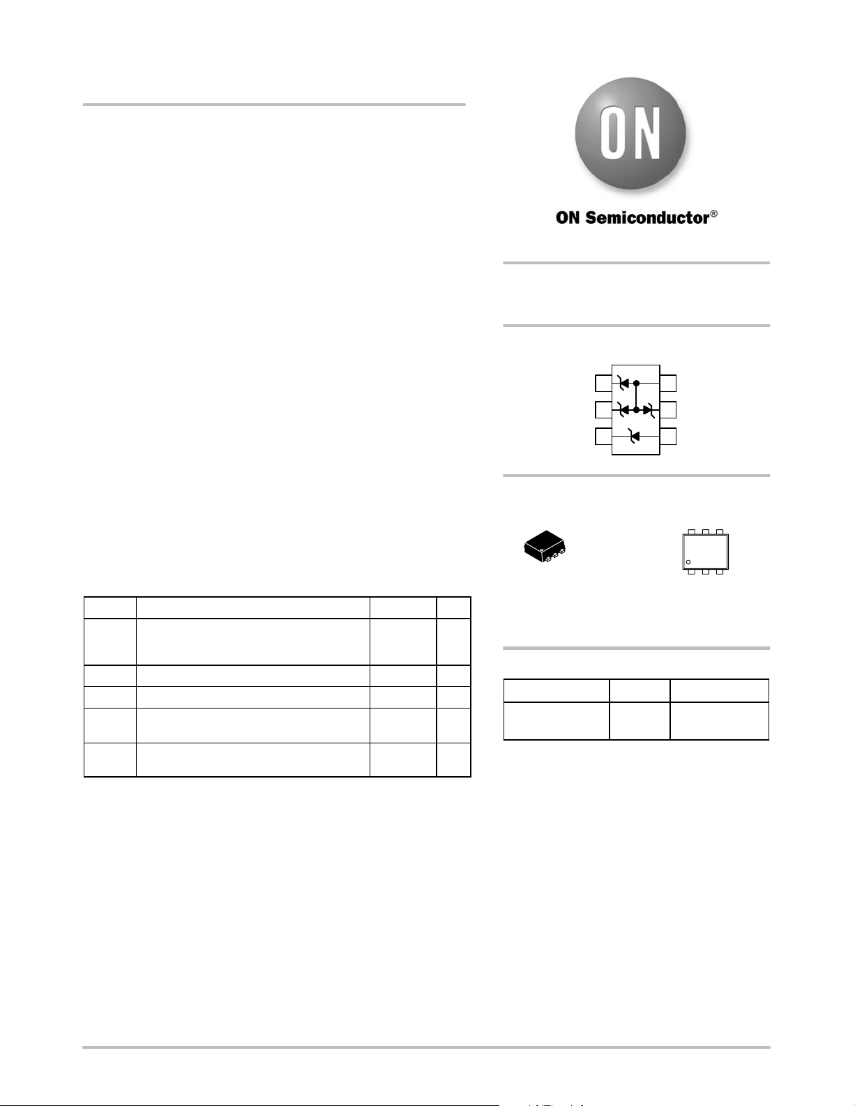
SOT−563 4−LINE TRANSIENT
VOLTAGE SUPPRESSOR
PIN ASSIGNMENT
D
1
1
D
2
2
V
CC
3
6
1
SOT−563
CASE 463A
STYLE 6
MT = Specific Device Code
M = Date Code
G = Pb−Free Package
(Note: Microdot may be in either location
ORDERING INFORMATION
Device Package Shipping
NUP4060AXV6T1G SOT−563
†For information on tape and reel specifications,
including part orientation and tape sizes, please
refer to our Tape and Reel Packaging Specification
Brochure, BRD8011/D.
(Pb−Free)
GND
6
D
5
3
GND
4
MARKING
DIAGRAM
MT MG
G
1
4000/Tape & Ree
†
© Semiconductor Components Industries, LLC, 2007
January , 2007 − Rev. 1
1 Publication Order Number:
NUP4060/D

NUP4060AXV6
ELECTRICAL CHARACTERISTICS (T
Parameter
= 25°C, unless otherwise specified)
J
Conditions Symbol Min Typ Max Unit
Reverse Working Voltage (D1, D2, and D3) (Note 2) V
Breakdown Voltage (D1, D2, and D3) IT = 1 mA, (Note 3) V
Breakdown Voltage (VCC) IT = 5 mA, (Note 3) V
Reverse Leakage Current (D1, D2, and D3) V
= 3 V I
RWM
Reverse Leakage Current (VCC) VBR = 11 V I
Capacitance (D1, D2, and D3) VR = 3 V, f = 1 MHz (Line to GND) C
2. TVS devices are normally selected according to the working peak reverse voltage (V
or continuous peak operating voltage level.
is measured at pulse test current IT.
3. V
BR
), which should be equal or greater than the DC
RWM
RWM
BR
BR2
R
R
J
− − 5.0 V
6.2 6.8 7.2 V
15.3 16 17.1 V
− 0.01 0.5
− − 0.05
− 7 10 pF
mA
mA
http://onsemi.com
2

TYPICAL ELECTRICAL CHARACTERISTICS
100
P
, PEAK SURGE POWER (W)
110
I
, REVERSE LEAKAGE (
A)
(Diode D
10
pk
1
1 10 100 1000
t, TIME (ms)
Figure 1. Pulse Width
NUP4060AXV6
, D2, and D3 only)
1
100
PP
90
80
70
60
50
40
30
20
% OF RATED POWER OR I
10
0
1501251007550250
TA, AMBIENT TEMPERATURE (°C)
Figure 2. Power Derating Curve
0.16
0.14
m
0.12
0.10
0.08
0.06
0.04
R
0.02
0
−60 0 80 100
100
t
r
90
80
70
60
50
40
30
20
% OF PEAK PULSE CURRENT
10
0
020406080
−40 −20 604020
T, TEMPERATURE (°C)
Figure 3. Reverse Leakage versus
Temperature
t
P
PEAK VALUE I
PULSE WIDTH (tP) IS DEFINED
AS THAT POINT WHERE THE
PEAK CURRENT DECAY = 8 ms
HALF VALUE I
t, TIME (ms)
RSM
@ 8 ms
RSM
/2 @ 20 ms
Figure 5. 8 × 20 ms Pulse Waveform
14
12
10
8
6
4
1 MHz FREQUENCY
TYPICAL CAPACITANCE (pF)
2
0
01 23 6
BIAS VOLTAGE (V)
TA = 25°C
45
Figure 4. Capacitance
1
0.1
0.01
, FORWARD CURRENT (A)
F
I
0.001
VF, FORWARD VOLTAGE (V)
TA = 25°C
Figure 6. Forward Voltage
1.81.61.41.21.00.80.6
http://onsemi.com
3

D
−X−
6
12 3
e
45
b
0.08 (0.003) X
E
−Y−
6 5 PL
NUP4060AXV6
PACKAGE DIMENSIONS
SOT−563, 6 LEAD
CASE 463A−01
ISSUE F
NOTES:
1. DIMENSIONING AND TOLERANCING PER ANSI
Y14.5M, 1982.
A
L
H
E
C
M
Y
SOLDERING FOOTPRINT*
0.3
0.0118
2. CONTROLLING DIMENSION: MILLIMETERS
3. MAXIMUM LEAD THICKNESS INCLUDES LEAD
FINISH THICKNESS. MINIMUM LEAD THICKNESS
IS THE MINIMUM THICKNESS OF BASE MATERIAL.
MILLIMETERS
DIM MIN NOM MAX
A 0.50 0.55 0.60
b 0.17 0.22 0.27
C
0.08 0.12 0.18 0.003 0.005 0.007
D 1.50 1.60 1.70
E 1.10 1.20 1.30
e 0.5 BSC
L 0.10 0.20 0.30
H
1.50 1.60 1.70
E
INCHES
MIN NOM MAX
0.020 0.021 0.023
0.007 0.009 0.011
0.059 0.062 0.066
0.043 0.047 0.051
0.02 BSC
0.004 0.008 0.012
0.059 0.062 0.066
0.45
0.0177
1.0
1.35
0.0394
0.0531
0.5
0.5
0.0197
0.0197
mm
ǒ
SCALE 20:1
inches
Ǔ
*For additional information on our Pb−Free strategy and soldering
details, please download the ON Semiconductor Soldering and
Mounting Techniques Reference Manual, SOLDERRM/D.
ON Semiconductor and are registered trademarks of Semiconductor Components Industries, LLC (SCILLC). SCILLC reserves the right to make changes without further notice
to any products herein. SCILLC makes no warranty, representation or guarantee regarding the suitability of its products for any particular purpose, nor does SCILLC assume any liability
arising out of the application or use of any product or circuit, and specifically disclaims any and all liability, including without limitation special, consequential or incidental damages.
“Typical” parameters which may be provided in SCILLC data sheets and/or specifications can and do vary in different applications and actual performance may vary over time. All
operating parameters, including “Typicals” must be validated for each customer application by customer’s technical experts. SCILLC does not convey any license under its patent rights
nor the rights of others. SCILLC products are not designed, intended, or authorized for use as components in systems intended for surgical implant into the body, or other applications
intended to support or sustain life, or for any other application in which the failure of the SCILLC product could create a situation where personal injury or death may occur. Should
Buyer purchase or use SCILLC products for any such unintended or unauthorized application, Buyer shall indemnify and hold SCILLC and its officers, employees, subsidiaries, affiliates,
and distributors harmless against all claims, costs, damages, and expenses, and reasonable attorney fees arising out of, directly or indirectly, any claim of personal injury or death
associated with such unintended or unauthorized use, even if such claim alleges that SCILLC was negligent regarding the design or manufacture of the part. SCILLC is an Equal
Opportunity/Affirmative Action Employer. This literature is subject to all applicable copyright laws and is not for resale in any manner.
PUBLICATION ORDERING INFORMATION
LITERATURE FULFILLMENT:
Literature Distribution Center for ON Semiconductor
P.O. Box 5163, Denver, Colorado 80217 USA
Phone: 303−675−2175 or 800−344−3860 Toll Free USA/Canada
Fax: 303−675−2176 or 800−344−3867 Toll Free USA/Canada
Email: orderlit@onsemi.com
N. American Technical Support: 800−282−9855 Toll Free
USA/Canada
Europe, Middle East and Africa Technical Support:
Phone: 421 33 790 2910
Japan Customer Focus Center
Phone: 81−3−5773−3850
http://onsemi.com
4
ON Semiconductor Website: www.onsemi.com
Order Literature: http://www.onsemi.com/orderlit
For additional information, please contact your local
Sales Representative
NUP4060/D

 Loading...