

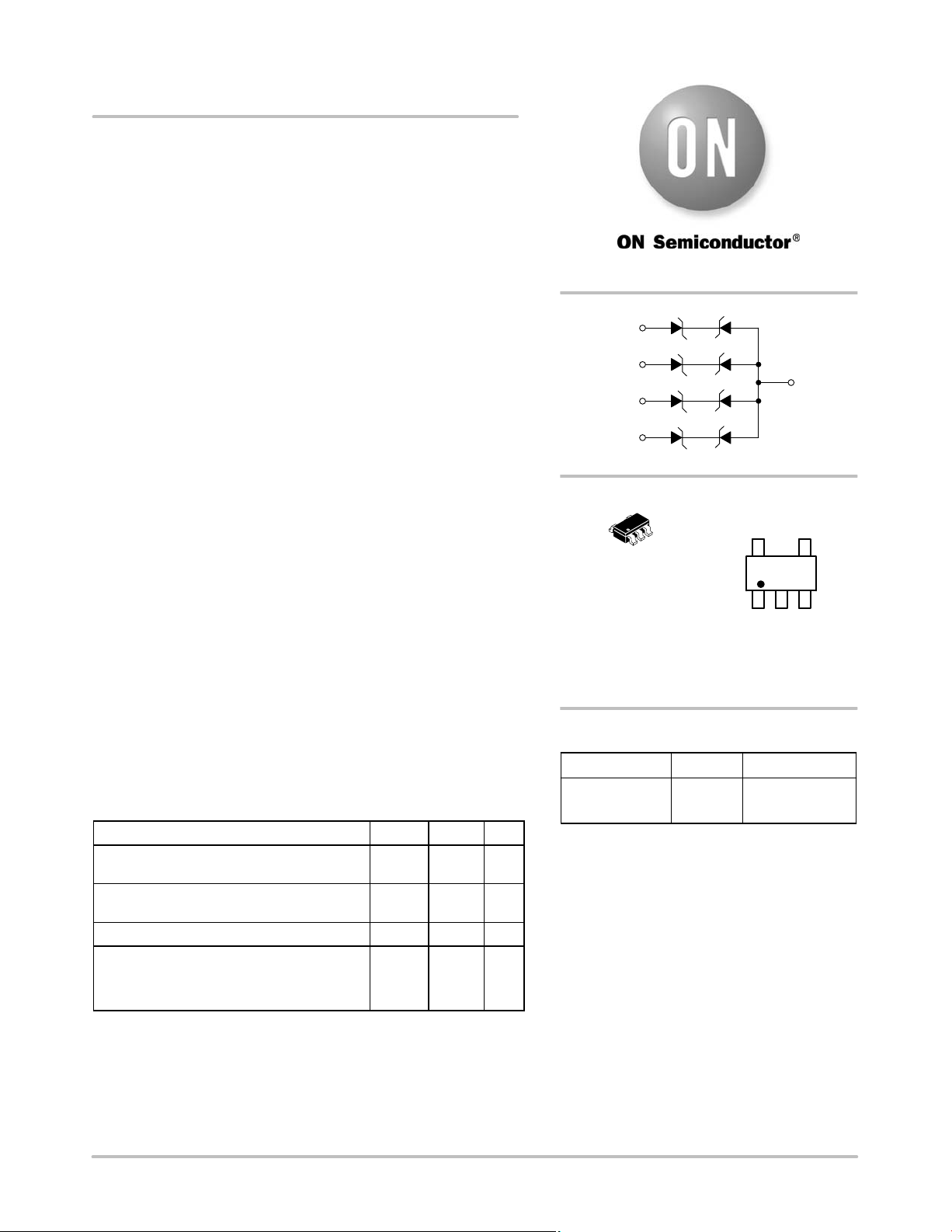
NUP4004M5
5-Pin Bi-Directional Quad
TVS Array
This 5-Pin bi-directional transient suppressor array is designed for
applications requiring transient overvoltage protection capability. It is
intended for use in transient voltage and ESD sensitive equipment
such as computers, printers, cell phones, medical equipment, and other
applications. Its integrated design provides bi-directional protection
for four separate lines using a single TSOP-5 package. This device is
ideal for situations where board space is a premium.
http://onsemi.com
http://onsemi.com
5
Features
•Bi-directional Protection for Four Lines in a Single TSOP-5 Package
•Low Leakage Current
•Low Capacitance
•Provides ESD Protection for JEDEC Standards JESD22
- Machine Model = Class C
- Human Body Model = Class 3B
•Provides ESD Protection for IEC 61000-4-2, 15 kV (Air),
8 kV (Contact)
•This is a Pb-Free Device
Mechanical Characteristics
•Void Free, Transfer-Molded, Thermosetting Plastic Case
•Corrosion Resistant Finish, Easily Solderable
•Package Designed for Optimal Automated Board Assembly
•Small Package Size for High Density Applications
Applications
•LCD, Plasma TV Video Lines
•Other Telephone Sets
•Computers / Printers / Set-Top Boxes
MAXIMUM RATINGS (T
Operating Junction Temperature Range T
Storage Temperature Range T
Lead Solder Temperature – Maximum (10 sec) T
Human Body Model ( HBM)
Machine Model (MM)
IEC 61000-4-2 Air (ESD)
IEC 61000-4-2 Contact (ESD)
Stresses exceeding Maximum Ratings may damage the device. Maximum
Ratings are stress ratings only. Functional operation above the Recommended
Operating Conditions is not implied. Extended exposure to stresses above the
Recommended Operating Conditions may affect device reliability.
=25°C, unless otherwise specified)
J
Rating Symbol Value Unit
-40 to
J
125
-55 to
STG
ESD 16
L
150
260 °C
0.4
30
30
°C
°C
kV
4
2
3
1
MARKING
DIAGRAM
5
1
TSOP-5
CASE 483
MY = Specific Device Code
M = Date Code
G = Pb-Free Package
(Note: Microdot may be in either location)
5
MY MG
G
1
ORDERING INFORMATION
Device Package Shipping
NUP4004M5T1G TSOP-5
(Pb-Free)
†For information on tape and reel specifications,
including part orientation and tape sizes, please
refer to our Tape and Reel Packaging Specification
Brochure, BRD8011/D.
3000/Tape & Reel
†
© Semiconductor Components Industries, LLC, 2008
February, 2008 - Rev. 2
1 Publication Order Number:
NUP4004M5/D
NUP4004M5
ELECTRICAL CHARACTERISTICS (T
Parameter
=25°C, unless otherwise specified)
J
Conditions Symbol Min Typ Max Unit
Reverse Working Voltage (Note 1) V
Breakdown Voltage IT = 1 mA, (Note 2) V
Reverse Leakage Current V
= 5 V I
RWM
Capacitance VR = -3 V, f = 1 MHz
(Line to GND)
Capacitance VR = 3 V, f = 1 MHz
(Line to GND)
1. TVS devices are normally selected according to the working peak reverse voltage (V
or continuous peak operating voltage level.
is measured at pulse test current IT.
2. V
BR
RWM
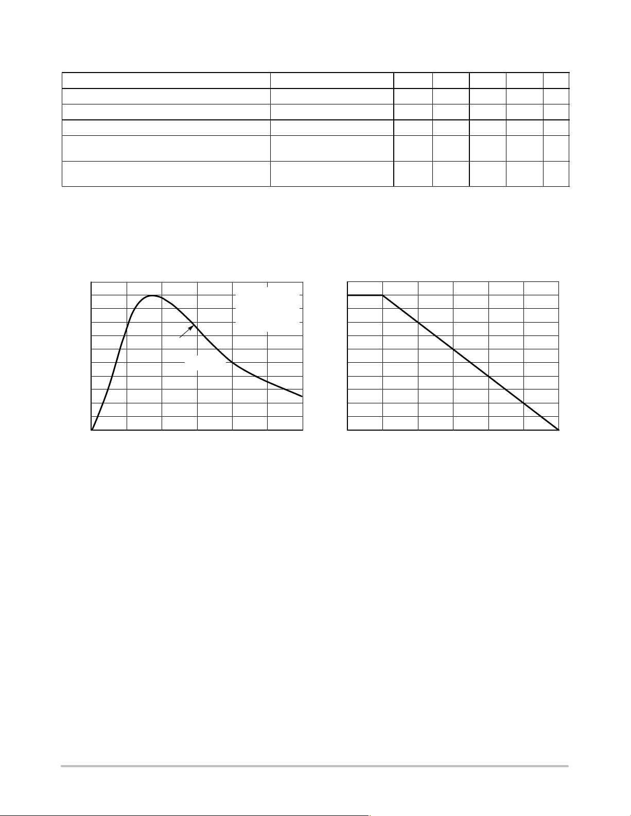
TYPICAL PERFORMANCE CURVES
(T
= 25°C unless otherwise specified)
J
110
100
90
80
PP
70
60
50
40
PERCENT OF I
30
20
10
0
c-t
td = IPP/2
t, TIME (ms)
WAVEFORM
PARAMETERS
t
= 8 ms
r
t
= 20 ms
d
2520
30151050
110
100
PP
90
80
70
60
50
40
30
20
% OF RATED POWER OR I
10
0
TA, AMBIENT TEMPERATURE (°C)
RWM
BR
R
C
j
C
j
7.0 8.0 V
100 1000 nA
23 pF
32 pF
5.0 V
), which should be equal or greater than the DC
1501251007550250
Figure 1. Pulse Waveform
Figure 2. Power Derating Curve
http://onsemi.com
2

NUP4004M5
PACKAGE DIMENSIONS
TSOP-5
CASE 483-02
ISSUE F
NOTES:
1. DIMENSIONING AND TOLERANCING PER
NOTE 5
2X
2X
T0.10
T0.20
54
123
L
G
D
0.205XC AB
M
S
B
K
DETAIL Z
A
J
DETAIL Z
C
0.05
H
SEATING
PLANE
T
ASME Y14.5M, 1994.
2. CONTROLLING DIMENSION: MILLIMETERS.
3. MAXIMUM LEAD THICKNESS INCLUDES
LEAD FINISH THICKNESS. MINIMUM LEAD
THICKNESS IS THE MINIMUM THICKNESS
OF BASE MATERIAL.
4. DIMENSIONS A AND B DO NOT INCLUDE
MOLD FLASH, PROTRUSIONS, OR GATE
BURRS.
5. OPTIONAL CONSTRUCTION: AN
ADDITIONAL TRIMMED LEAD IS ALLOWED
IN THIS LOCATION. TRIMMED LEAD NOT TO
EXTEND MORE THAN 0.2 FROM BODY.
MILLIMETERS
DIM MIN MAX
A 3.00 BSC
B 1.50 BSC
C 0.90 1.10
D 0.25 0.50
G 0.95 BSC
H 0.01 0.10
J 0.10 0.26
K 0.20 0.60
L 1.25 1.55
M 0 10
__
S 2.50 3.00
SOLDERING FOOTPRINT*
1.9
0.95
0.037
1.0
0.039
*For additional information on our Pb-Free strategy and soldering
details, please download the ON Semiconductor Soldering and
Mounting Techniques Reference Manual, SOLDERRM/D.
ON Semiconductor and are registered trademarks of Semiconductor Components Industries, LLC (SCILLC). SCILLC reserves the right to make changes without further notice
to any products herein. SCILLC makes no warranty, representation or guarantee regarding the suitability of its products for any particular purpose, nor does SCILLC assume any liability
arising out of the application or use of any product or circuit, and specifically disclaims any and all liability, including without limitation special, consequential or incidental damages.
“Typical” parameters which may be provided in SCILLC data sheets and/or specifications can and do vary in different applications and actual performance may vary over time. All
operating parameters, including “Typicals” must be validated for each customer application by customer's technical experts. SCILLC does not convey any license under its patent rights
nor the rights of others. SCILLC products are not designed, intended, or authorized for use as components in systems intended for surgical implant into the body, or other applications
intended to support or sustain life, or for any other application in which the failure of the SCILLC product could create a situation where personal injury or death may occur. Should
Buyer purchase or use SCILLC products for any such unintended or unauthorized application, Buyer shall indemnify and hold SCILLC and its officers, employees, subsidiaries, affiliates,
and distributors harmless against all claims, costs, damages, and expenses, and reasonable attorney fees arising out of, directly or indirectly, any claim of personal injury or death
associated with such unintended or unauthorized use, even if such claim alleges that SCILLC was negligent regarding the design or manufacture of the part. SCILLC is an Equal
Opportunity/Affirmative Action Employer. This literature is subject to all applicable copyright laws and is not for resale in any manner.
0.074
0.028
0.7
2.4
0.094
SCALE 10:1
ǒ
inches
mm
Ǔ
PUBLICATION ORDERING INFORMATION
LITERATURE FULFILLMENT:
Literature Distribution Center for ON Semiconductor
P.O. Box 5163, Denver, Colorado 80217 USA
Phone: 303-675-2175 or 800-344-3860 Toll Free USA/Canada
Fax: 303-675-2176 or 800-344-3867 Toll Free USA/Canada
Email: orderlit@onsemi.com
N. American Technical Support: 800-282-9855 Toll Free
USA/Canada
Europe, Middle East and Africa Technical Support:
Phone: 421 33 790 2910
Japan Customer Focus Center
Phone: 81-3-5773-3850
http://onsemi.com
3
ON Semiconductor Website: www.onsemi.com
Order Literature: http://www.onsemi.com/orderlit
For additional information, please contact your local
Sales Representative
NUP4004M5/D

 Loading...