

Page 1
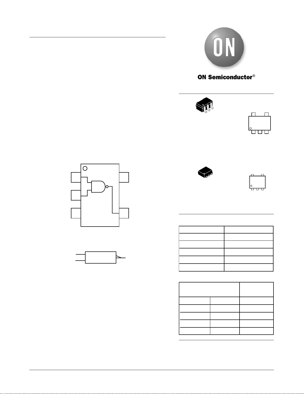
NL17SZ00
Single 2−Input NAND Gate
The NL17SZ00 is a single 2−input NAND Gate in two tiny footprint
packages. The device performs much as LCX multi−gate products in
speed and drive.
Features
• Tiny SOT−353 and SOT−553 Packages
• 2.7 ns T
at 5 V (typ)
PD
• Source/Sink 24 mA at 3.0 V
• Over−Voltage Tolerant Inputs
• Pin For Pin with NC7SZ00P5X, TC7SZ00FU and TC7SZ00AFE
• Chip Complexity: FET s = 20
• Designed for 1.65 V to 5.5 V V
Operation
CC
• Pb−Free Packages are Available
5
V
CC
4
Y
GND
A
1
B
2
3
http://onsemi.com
5
1
SOT−353/SC70−5/SC−88A
DF SUFFIX
CASE 419A
L1 = Specific Device Marking
M = Date Code
G = Pb−Free Package
(Note: Microdot may be in either location)
5
1
SOT−553
XV5 SUFFIX
CASE 463B
L1 = Specific Device Marking
M = Date Code
PIN ASSIGNMENT
MARKING
DIAGRAMS
5
L1 MG
G
1
5
L1 M
1
Figure 1. Pinout (Top View)
A
B
Figure 2. Logic Symbol
© Semiconductor Components Industries, LLC, 2006
November, 2006 − Rev. 5
Pin
1
2
3
&
Y
4
5
Function
A
B
GND
Y
V
CC
FUNCTION TABLE
Output
Input
A
L
L
H
H
B
L
H
L
H
Y = AB
Y
H
H
H
L
ORDERING INFORMATION
See detailed ordering and shipping information in the package
dimensions section on page 4 of this data sheet.
1 Publication Order Number:
NL17SZ00/D
Page 2
NL17SZ00
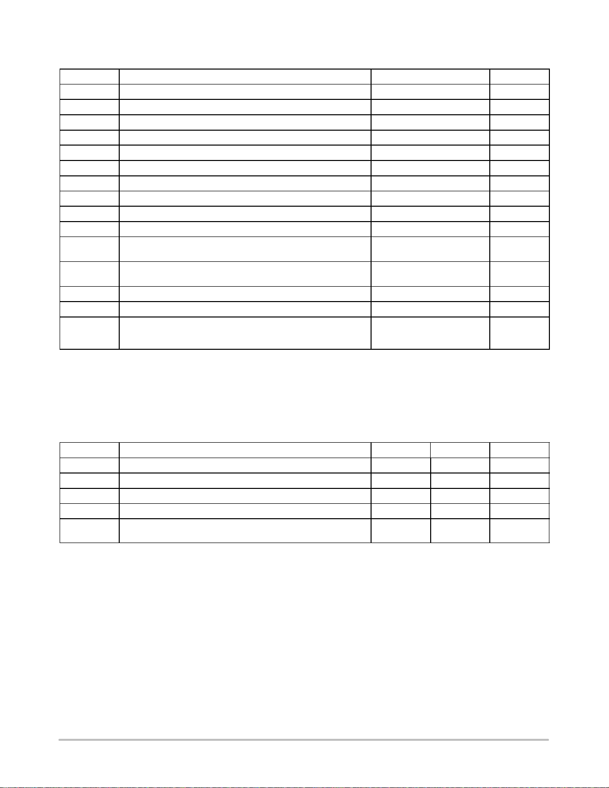
MAXIMUM RATINGS
Symbol Parameter Value Unit
V
CC
V
IN
V
OUT
I
IK
I
OK
I
OUT
I
CC
T
STG
T
L
T
J
q
JA
P
D
MSL Moisture Sensitivity Level 1
F
R
ESD ESD Classification Human Body Model (Note 2)
Stresses exceeding Maximum Ratings may damage the device. Maximum Ratings are stress ratings only. Functional operation above the
Recommended Opera t i n g Conditions is not implied. Extended exposure to stresses above the Recommended Operating Conditions may affect
device reliability.
1. Measured with minimum pad spacing on an FR4 board, using 10 mm−by−1 inch, 2−ounce copper trace with no air flow.
2. Tested to EIA/JESD22−A114−A, rated to EIA/JESD22−A114−B.
3. Tested to EIA/JESD22−A115−A, rated to EIA/JESD22−A115−A.
4. Tested to JESD22−C101−A.
DC Supply Voltage *0.5 to )7.0 V
DC Input Voltage *0.5 to )7.0 V
DC Output Voltage *0.5 to to VCC + 0.5 V
DC Input Diode Current *50 mA
DC Output Diode Current *50 mA
DC Output Sink Current $50 mA
DC Supply Current per Supply Pin $100 mA
Storage Temperature Range *65 to )150 °C
Lead Temperature, 1 mm from Case for 10 Seconds 260 °C
Junction Temperature Under Bias )150 °C
Thermal Resistance SOT−353 (Note 1)
SOT−553
Power Dissipation in Still Air at 85°C SOT−353
SOT−553
350
496
186
135
°C/W
mW
Flammability Rating Oxygen Index: 28 to 34 UL 94 V−0 @ 0.125 in
Class Z
Machine Model (Note 3)
Charged Device Model (Note 4)
Class A
N/A
RECOMMENDED OPERATING CONDITIONS
Symbol Parameter Min Max Unit
V
V
V
T
tr, t
CC
IN
OUT
A
f
DC Supply Voltage 1.65 5.5 V
DC Input Voltage 0 5.5 V
DC Output Voltage 0 VCC + 0.5 V
Operating Temperature Range *40 )85 °C
Input Rise and Fall Time VCC = 3.0 V $0.3 V
V
= 5.0 V $0.5 V
CC
0
0
100
20
ns/V
http://onsemi.com
2
Page 3
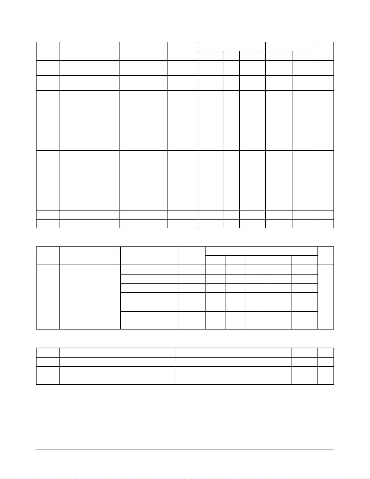
DC ELECTRICAL CHARACTERISTICS
l
t
l
t
Symbo
V
IH
V
IL
V
OH
V
OL
I
IN
I
CC
Parameter Condition
High−Level Input Voltage 1.65 to 1.95
Low−Level Input Voltage 1.65 to 1.95
High−Level Output Voltage
IN
= V
or V
IL
IH
V
Low−Level Output Voltage
IN
= V
or V
IH
OH
V
IOH = 100 mA
I
I
I
OH
I
OH
I
OH
I
OH
IOL = 100 mA
I
I
I
I
Input Leakage Current VIN = VCC or GND 0 to 5.5 $0.1 $1.0
Quiescent Supply Current VIN = VCC or GND 5.5 1 10
= −3 mA
OH
= −8 mA
OH
= −12 mA
= −16 mA
= −24 mA
= −32 mA
I
= 3 mA
OL
I
= 8 mA
OL
= 12 mA
OL
= 16 mA
OL
= 24 mA
OL
= 32 mA
OL
NL17SZ00
V
CC
(V)
2.3 to 5.5
2.3 to 5.5
1.65 to 5.5
1.65
2.3
2.7
3.0
3.0
4.5
1.65 to 5.5
1.65
2.3
2.7
3.0
3.0
4.5
TA = 255C *405C v TA v 855C
Min Typ Max Min Max
0.75 V
CC
0.7 V
CC
VCC − 0.1
1.55
1.9
2.2
2.4
2.3
3.8
V
CC
1.65
2.1
2.4
2.7
2.5
4.0
0.25 V
0.3 V
CC
CC
0.75 V
CC
0.7 V
CC
VCC − 0.1
1.55
1.9
2.2
2.4
2.3
3.8
0.1
0.08
0.20
0.22
0.28
0.38
0.42
0.24
0.3
0.4
0.4
0.55
0.55
0.25 V
0.3 V
0.1
0.24
0.3
0.4
0.4
0.55
0.55
CC
CC
Uni
V
V
V
V
mA
mA
AC ELECTRICAL CHARACTERISTICS t
Symbo
t
PLH
t
PHL
Parameter Condition
Propagation Delay
(Figure 3 and 4)
RL = 1 MW, C
RL = 1 MW, C
RL = 1 MW, C
RL = 1 MW, C
RL = 500 W, C
RL = 1 MW, C
RL = 500 W, C
= tF = 3.0 ns
R
= 15 pF
L
= 15 pF
L
= 15 pF
L
= 15 pF
L
= 50 pF
L
= 15 pF
L
= 50 pF
L
V
CC
(V)
TA = 255C *405C v TA v 855C
Min Typ Max Min Max
1.65 2.0 5.4 11.4 2.0 12
1.8 2.0 4.5 9.5 2.0 10.0
2.5 to 0.2 0.8 3.0 6.5 0.8 7.0
3.3 $ 0.3
0.5 2.4 4.5 0.5 4.7
1.5 2.4 5.0 1.5 5.2
5.0 $ 0.5
0.5 2.0 3.9 0.5 4.1
0.8 2.4 4.3 0.8 4.5
Uni
ns
CAPACITIVE CHARACTERISTICS
Symbol Parameter Condition Typical Unit
C
C
5. CPD is defined as the value of the internal equivalent capacitance which is calculated from the operating current consumption without load.
Average operating current can be obtained by the equation: I
power consumption; P
Input Capacitance VCC = 5.5 V, VI = 0 V or V
IN
Power Dissipation Capacitance
PD
(Note 5)
D
= CPD V
2
fin + ICC VCC.
CC
10 MHz, VCC = 3.3 V, VI = 0 V or V
10 MHz, VCC = 5.5 V, VI = 0 V or V
= CPD VCC fin + ICC. CPD is used to determine the no−load dynamic
)
CC(OPR
CC
CC
CC
u4 pF
25
pF
30
http://onsemi.com
3
Page 4
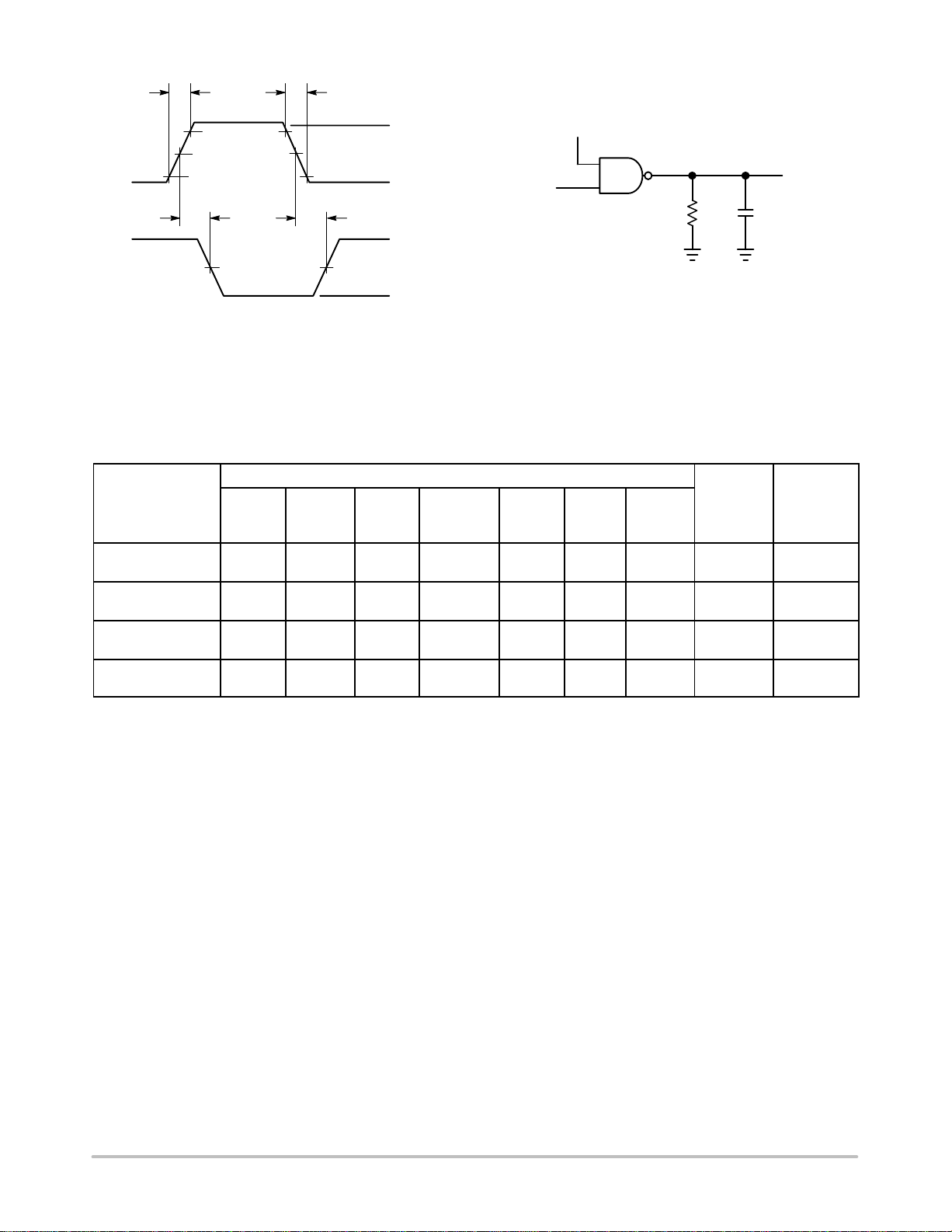
NL17SZ00
tf = 3 ns
INPUT
A and B
OUTPUT Y
90%
90%
t
PHL
50%
10%
50%
50%
Figure 3. Switching Waveform
t
50%
PLH
10%
tf = 3 ns
V
CC
GND
V
OH
V
OL
V
CC
INPUT
R
L
A 1−MHz square input wave is recommended for
propagation delay tests.
Figure 4. Test Circuit
C
OUTPUT
L
DEVICE ORDERING INFORMATION
Device Nomenclature
Logic
Device Order
Number
Circuit
Indicator
NL17SZ00DFT2 NL 1 7 SZ 00 DF T2 SOT−353 178 mm,
NL17SZ00DFT2G NL 1 7 SZ 00 DF T2 SOT−353
NL17SZ00XV5T2 NL 1 7 SZ 00 XV5 T2 SOT−553* 178 mm
NL17SZ00XV5T2G NL 1 7 SZ 00 XV5 T2 SOT−553* 178 mm
†For information on tape and reel specifications, including part orientation and tape sizes, please refer to our Tape and Reel Packaging
Specifications Brochure, BRD8011/D.
*All Devices in Package SOT553 are Inherently Pb−Free.
No. of
Gates per
Package
Temp
Range
Identifier
Technology
Device
Function
Package
Suffix
Tape and
Reel
Suffix
Package
Type
(Pb−Free)
Tape and
Reel Size
3000 Units
178 mm,
3000 Units
4000 units
4000 units
†
http://onsemi.com
4
Page 5

NL17SZ00
PACKAGE DIMENSIONS
SOT−353
(SC−88A, SC−70)
DF SUFFIX
CASE 419A−02
ISSUE J
A
G
45
D
5 PL
−B−
MM
B0.2 (0.008)
S
12 3
N
J
C
NOTES:
1. DIMENSIONING AND TOLERANCING
PER ANSI Y14.5M, 1982.
2. CONTROLLING DIMENSION: INCH.
3. 419A−01 OBSOLETE. NEW STANDARD
419A−02.
4. DIMENSIONS A AND B DO NOT INCLUDE
MOLD FLASH, PROTRUSIONS, OR GATE
BURRS.
INCHES
DIMAMIN MAX MIN MAX
B 1.15 1.350.045 0.053
C 0.80 1.100.031 0.043
D 0.10 0.300.004 0.012
G 0.65 BSC0.026 BSC
H −−− 0.10−−−0.004
J 0.10 0.250.004 0.010
K 0.10 0.300.004 0.012
N 0.20 REF0.008 REF
S 2.00 2.200.079 0.087
MILLIMETERS
1.80 2.200.071 0.087
H
K
SOLDERING FOOTPRINT*
0.50
0.0197
0.65
0.025
0.65
0.40
0.0157
1.9
0.0748
SCALE 20:1
*For additional information on our Pb−Free strategy and soldering
details, please download the ON Semiconductor Soldering and
Mounting Techniques Reference Manual, SOLDERRM/D.
0.025
mm
ǒ
inches
Ǔ
http://onsemi.com
5
Page 6

NL17SZ00
PACKAGE DIMENSIONS
SOT−553
XV5 SUFFIX
CASE 463B−01
ISSUE B
D
−X−
45
12 3
e
NOTES:
1. DIMENSIONING AND TOLERANCING PER ANSI Y14.5M, 1982.
2. CONTROLLING DIMENSION: MILLIMETERS
3. MAXIMUM LEAD THICKNESS INCLUDES LEAD FINISH
THICKNESS. MINIMUM LEAD THICKNESS IS THE MINIMUM
THICKNESS OF BASE MATERIAL.
DIMAMIN NOM MAX MIN
b 0.17 0.22 0.27 0.007
c
D 1.50 1.60 1.70 0.059
E 1.10 1.20 1.30 0.043
e 0.50 BSC
L 0.10 0.20 0.30 0.004
H
E
E
−Y−
b
5 PL
0.08 (0.003) X
M
A
L
H
E
c
Y
SOLDERING FOOTPRINT*
0.3
0.0118
0.45
0.0177
1.0
1.35
0.0531
*For additional information on our Pb−Free strategy and soldering
details, please download the ON Semiconductor Soldering and
Mounting Techniques Reference Manual, SOLDERRM/D.
0.0394
0.5
0.0197
0.5
0.0197
SCALE 20:1
MILLIMETERS
0.50 0.55 0.60 0.020
0.08 0.13 0.18
1.50 1.60 1.70 0.059 0.063 0.067
mm
ǒ
Ǔ
inches
INCHES
NOM MAX
0.022 0.024
0.009 0.011
0.003 0.005 0.007
0.063 0.067
0.047 0.051
0.020 BSC
0.008 0.012
ON Semiconductor and are registered trademarks of Semiconductor Components Industries, LLC (SCILLC). SCILLC reserves the right to make changes without further notice
to any products herein. SCILLC makes no warranty, representation or guarantee regarding the suitability of its products for any particular purpose, nor does SCILLC assume any liability
arising out of the application or use of any product or circuit, and specifically disclaims any and all liability, including without limitation special, consequential or incidental damages.
“Typical” parameters which may be provided in SCILLC data sheets and/or specifications can and do vary in different applications and actual performance may vary over time. All
operating parameters, including “Typicals” must be validated for each customer application by customer’s technical experts. SCILLC does not convey any license under its patent rights
nor the rights of others. SCILLC products are not designed, intended, or authorized for use as components in systems intended for surgical implant into the body, or other applications
intended to support or sustain life, or for any other application in which the failure of the SCILLC product could create a situation where personal injury or death may occur. Should
Buyer purchase or use SCILLC products for any such unintended or unauthorized application, Buyer shall indemnify and hold SCILLC and its officers, employees, subsidiaries, affiliates,
and distributors harmless against all claims, costs, damages, and expenses, and reasonable attorney fees arising out of, directly or indirectly, any claim of personal injury or death
associated with such unintended or unauthorized use, even if such claim alleges that SCILLC was negligent regarding the design or manufacture of the part. SCILLC is an Equal
Opportunity/Affirmative Action Employer. This literature is subject to all applicable copyright laws and is not for resale in any manner.
PUBLICATION ORDERING INFORMATION
LITERATURE FULFILLMENT:
Literature Distribution Center for ON Semiconductor
P.O. Box 5163, Denver, Colorado 80217 USA
Phone: 303−675−2175 or 800−344−3860 Toll Free USA/Canada
Fax: 303−675−2176 or 800−344−3867 Toll Free USA/Canada
Email: orderlit@onsemi.com
N. American Technical Support: 800−282−9855 Toll Free
USA/Canada
Europe, Middle East and Africa Technical Support:
Phone: 421 33 790 2910
Japan Customer Focus Center
Phone: 81−3−5773−3850
http://onsemi.com
ON Semiconductor Website: www.onsemi.com
Order Literature: http://www.onsemi.com/orderlit
For additional information, please contact your local
Sales Representative
NL17SZ00/D
6
Page 7

 Loading...