

ON Semiconductor
High Voltage Transistor
NPN Silicon
MAXIMUM RATINGS
Rating Symbol Value Unit
Collector–Emitter Voltage V
Collector–Base Voltage V
Emitter–Base Voltage V
Base Current I
Collector Current — Continuous I
THERMAL CHARACTERISTICS
Characteristic Symbol Max Unit
Total Device Dissipation FR–5 Board
TA = 25°C
Derate above 25°C
Thermal Resistance, Junction to Ambient R
Total Device Dissipation
Alumina Substrate,
Derate above 25°C
Thermal Resistance, Junction to Ambient R
Junction and Storage Temperature TJ, T
(2)
TA = 25°C
(1)
DEVICE MARKING
MMBT6517LT1 = 1Z
CEO
CBO
EBO
B
C
P
D
JA
P
D
JA
stg
350 Vdc
350 Vdc
5.0 Vdc
250 mAdc
500 mAdc
225
1.8
556 °C/W
300
2.4
417 °C/W
–55 to +150 °C
mW
mW/°C
mW
mW/°C
MMBT6517LT1
3
1
2
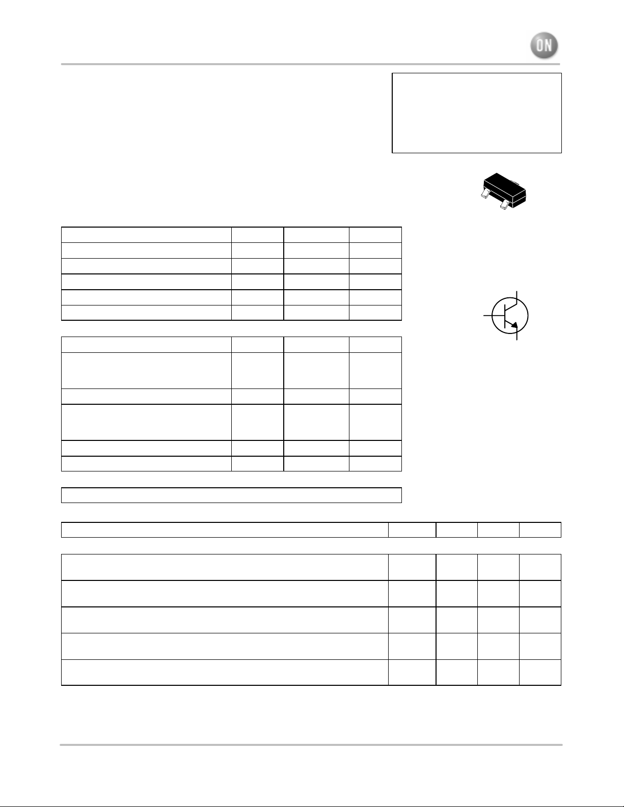
CASE 318–08, STYLE 6
SOT–23 (TO–236AB)
COLLECTOR
3
1
BASE
2
EMITTER
ELECTRICAL CHARACTERISTICS (T
Characteristic Symbol Min Max Unit
= 25°C unless otherwise noted)
A
OFF CHARACTERISTICS
Collector–Emitter Breakdown Voltage
(IC = 1.0 mAdc)
Collector–Base Breakdown Voltage
(IC = 100 Adc)
Emitter–Base Breakdown Voltage
(IE = 10 Adc)
Collector Cutoff Current
(VCB = 250 Vdc)
Emitter Cutoff Current
(VEB = 5.0 Vdc)
1. FR–5 = 1.0 0.75 0.062 in.
2. Alumina = 0.4 0.3 0.024 in. 99.5% alumina.
Semiconductor Components Industries, LLC, 2001
November, 2001 – Rev. 2
V
(BR)CEO
V
(BR)CBO
V
(BR)EBO
I
CBO
I
EBO
1 Publication Order Number:
350 —
350 —
6.0 —
— 50
— 50
MMBT6517LT1/D
Vdc
Vdc
Vdc
nAdc
nAdc

MMBT6517LT1
ELECTRICAL CHARACTERISTICS (T
Characteristic Symbol Min Max Unit
= 25°C unless otherwise noted) (Continued)
A
ON CHARACTERISTICS
DC Current Gain
(IC = 1.0 mAdc, VCE = 10 Vdc)
(IC = 10 mAdc, VCE = 10 Vdc)
(IC = 30 mAdc, VCE = 10 Vdc)
(IC = 50 mAdc, VCE = 10 Vdc)
(IC = 100 mAdc, VCE = 10 Vdc)
Collector–Emitter Saturation Voltage (3)
(IC = 10 mAdc, IB = 1.0 mAdc)
(IC = 20 mAdc, IB = 2.0 mAdc)
(IC = 30 mAdc, IB = 3.0 mAdc)
(IC = 50 mAdc, IB = 5.0 mAdc)
Base–Emitter Saturation Voltage
(IC = 10 mAdc, IB = 1.0 mAdc)
(IC = 20 mAdc, IB = 2.0 mAdc)
(IC = 30 mAdc, IB = 3.0 mAdc)
Base–Emitter On Voltage
(IC = 100 mAdc, VCE = 10 Vdc)
SMALL–SIGNAL CHARACTERISTICS
Current Gain — Bandwidth Product
(IC = 10 mAdc, VCE = 20 Vdc, f = 20 MHz)
Collector–Base Capacitance
(VCB = 20 Vdc, f = 1.0 MHz)
Emitter–Base Capacitance
(VEB = 0.5 Vdc, f = 1.0 MHz)
3. Pulse Test: Pulse Width = 300 s, Duty Cycle = 2.0%.
h
FE
V
CE(sat)
V
BE(sat)
V
BE(on)
f
C
C
T
cb
eb
20
30
30
20
15
—
—
—
—
—
—
—
— 2.0
40 200
— 6.0
— 80
—
—
200
200
—
0.30
0.35
0.50
1.0
0.75
0.85
0.90
—
Vdc
Vdc
Vdc
MHz
pF
pF
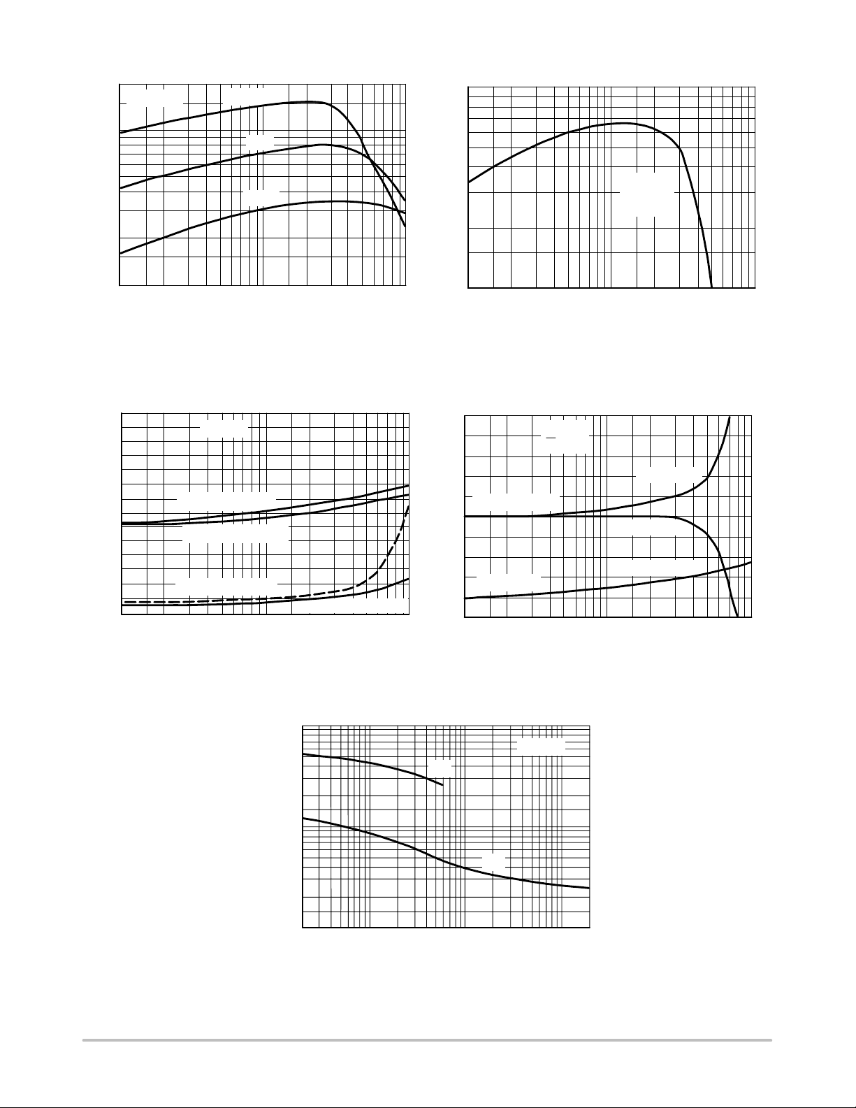
Figure 1.
http://onsemi.com
2
MMBT6517LT1
200
100
, DC CURRENT GAIN
FE
h
V, VOLTAGE (VOLTS)
70
50
30
20
10
1.4
1.2
1.0
0.8
0.6
0.4
0.2
0
VCE = 10 V
T
= 125°C
J
25°C
-55°C
IC, COLLECTOR CURRENT (mA)
Figure 1. DC Current Gain
T
= 25°C
J
V
@ IC/IB = 10
BE(sat)
V
@ VCE = 10 V
BE(on)
V
@ IC/IB = 10
CE(sat)
V
IC, COLLECTOR CURRENT (mA)
Figure 3. “On” Voltages
CE(sat)
@ IC/IB = 5.0
100
70
50
T
= 25°C
30
20
10
1001.0 2.0 3.0 5.0 7.0 10 20 30 50 70
T
f, CURRENT-GAIN BANDWIDTH PRODUCT (MHz)
IC, COLLECTOR CURRENT (mA)
J
VCE = 20 V
f = 20 MHz
1001.0 2.0 3.0 5.0 7.0 10 20 30 50 70
Figure 2. Current–Gain — Bandwidth Product
2.5
2.0
1.5
1.0
0.5
R
for V
θVC
0
-0.5
-1.0
-1.5
R
, TEMPERATURE COEFFICIENTS (mV/ C)°
-2.0
V
θ
R
-2.5
1001.0 2.0 3.0 5.0 7.0 10 20 30 50 70
θVB
I
C
10
I
B
CE(sat)
for V
BE
IC, COLLECTOR CURRENT (mA)
25°C to 125°C
-55°C to 25°C
-55°C to 125°C
1001.0 2.0 3.0 5.0 7.0 10 20 30 50 70
Figure 4. Temperature Coefficients
100
70
50
30
20
10
7.0
5.0
C, CAPACITANCE (pF)
3.0
2.0
1.0
C
eb
C
cb
VR, REVERSE VOLTAGE (VOLTS)
Figure 5. Capacitance
http://onsemi.com
3
T
= 25°C
J
2000.2 0.5 1.0 2.0 5.0 10 20 50 100

MMBT6517LT1
t, TIME (ns)
1.0k
700
500
300
200
100
10k
1001.0 2.0 3.0 5.0 7.0 10 20 30 50 70
CE(off)
1.0 k
7.0k
5.0k
3.0k
2.0k
1.0k
700
t, TIME (ns)
500
300
200
100
= 100 V
+V
CC
2.2 k
t
s
t
f
IC, COLLECTOR CURRENT (mA)
Figure 7. Turn–Off Time
20 k
50 Ω SAMPLING SCOPE
50
V
CE(off)
IC/IB = 5.0
IB1 = I
B2
T
= 25°C
J
= 100 V
1001.0 2.0 3.0 5.0 7.0 10 20 30 50 70
V
= 100 V
CE(off)
td @ V
t
r
70
50
30
20
10
IC, COLLECTOR CURRENT (mA)
BE(off)
= 2.0 V
IC/IB = 5.0
T
= 25°C
J
Figure 6. Turn–On Time
VCC ADJUSTED
+10.8 V
FOR V
PULSE WIDTH ≈ 100 µs
tr, t
≤ 5.0 ns
f
DUTY CYCLE ≤ 1.0%
FOR PNP TEST CIRCUIT,
REVERSE ALL VOLTAGE POLARITIES
1.0
0.7
D = 0.5
0.5
0.2
0.3
0.2
0.1
0.07
0.05
0.03
r(t), TRANSIENT THERMAL
RESISTANCE (NORMALIZED)
0.02
0.01
0.1
0.05
Z
θJC(t)
Z
θJA(t)
-9.2 V
SINGLE PULSE
SINGLE PULSE
= r(t) • R
θJC
= r(t) • R
θJA
1/2MSD7000
APPROXIMATELY
-1.35 V
(ADJUST FOR V
Figure 8. Switching Time Test Circuit
P
(pk)
DUTY CYCLE, D = t1/t
t, TIME (ms)
= 2.0 V)
(BE)off
R
(t) = r(t) R
θJC
D CURVES APPLY FOR POWER
t
1
t
2
PULSE TRAIN SHOWN
READ TIME AT t
T
J(pk)
2
- TC = P
θJC
1
(pk)
R
(t)
θJC
10k0.1 0.2 0.5 1.0 2.0 5.0 10 20 50 100 200 500 1.0k 2.0k 5.0k
Figure 9. Thermal Response
http://onsemi.com
4

MMBT6517LT1
INFORMATION FOR USING THE SOT–23 SURFACE MOUNT PACKAGE
MINIMUM RECOMMENDED FOOTPRINT FOR SURFACE MOUNTED APPLICATIONS
Surface mount board layout is a critical portion of the
total design. The footprint for the semiconductor packages
must be the correct size to insure proper solder connection
0.037
0.95
0.035
0.9
SOT–23 POWER DISSIPATION
The power dissipation of the SOT–23 is a function of the
pad size. This can vary from the minimum pad size for
soldering to a pad size given for maximum power dissipation. Power dissipation for a surface mount device is determined by T
of the die, R
, the maximum rated junction temperature
J(max)
, the thermal resistance from the device
θJA
junction to ambient, and the operating temperature, TA.
Using the values provided on the data sheet for the SOT–23
package, PD can be calculated as follows:
PD =
T
J(max)
R
θJA
– T
A
The values for the equation are found in the maximum
ratings table on the data sheet. Substituting these values
into the equation for an ambient temperature TA of 25°C,
one can calculate the power dissipation of the device which
in this case is 225 milliwatts.
150°C – 25°C
PD =
556°C/W
= 225 milliwatts
The 556°C/W for the SOT–23 package assumes the use
of the recommended footprint on a glass epoxy printed
circuit board to achieve a power dissipation of 225 milliwatts. There are other alternatives to achieving higher
power dissipation from the SOT–23 package. Another
alternative would be to use a ceramic substrate or an
aluminum core board such as Thermal Clad. Using a
board material such as Thermal Clad, an aluminum core
board, the power dissipation can be doubled using the same
footprint.
0.031
0.8
SOT–23
interface between the board and the package. With the
correct pad geometry, the packages will self align when
subjected to a solder reflow process.
0.037
0.95
0.079
2.0
inches
mm
SOLDERING PRECAUTIONS
The melting temperature of solder is higher than the
rated temperature of the device. When the entire device is
heated to a high temperature, failure to complete soldering
within a short time could result in device failure. Therefore, the following items should always be observed in
order to minimize the thermal stress to which the devices
are subjected.
• Always preheat the device.
• The delta temperature between the preheat and
soldering should be 100°C or less.*
• When preheating and soldering, the temperature of the
leads and the case must not exceed the maximum
temperature ratings as shown on the data sheet. When
using infrared heating with the reflow soldering
method, the difference shall be a maximum of 10°C.
• The soldering temperature and time shall not exceed
260°C for more than 10 seconds.
• When shifting from preheating to soldering, the
maximum temperature gradient shall be 5°C or less.
• After soldering has been completed, the device should
be allowed to cool naturally for at least three minutes.
Gradual cooling should be used as the use of forced
cooling will increase the temperature gradient and
result in latent failure due to mechanical stress.
• Mechanical stress or shock should not be applied
during cooling.
* Soldering a device without preheating can cause excessive thermal shock and stress which can result in damage
to the device.
http://onsemi.com
5

MMBT6517LT1
PACKAGE DIMENSIONS
SOT–23 (TO–236)
CASE 318–08
ISSUE AF
NOTES:
1. DIMENSIONING AND TOLERANCING PER ANSI
Y14.5M, 1982.
2. CONTROLLING DIMENSION: INCH.
A
L
3
1
2
S
B
GV
C
D
H
K
STYLE 6:
PIN 1. BASE
J
2. EMITTER
3. COLLECTOR
3. MAXIMUM LEAD THICKNESS INCLUDES LEAD
FINISH THICKNESS. MINIMUM LEAD THICKNESS
IS THE MINIMUM THICKNESS OF BASE
MATERIAL.
INCHES
DIMAMIN MAX MIN MAX
0.1102 0.1197 2.80 3.04
B 0.0472 0.0551 1.20 1.40
C 0.0350 0.0440 0.89 1.11
D 0.0150 0.0200 0.37 0.50
G 0.0701 0.0807 1.78 2.04
H 0.0005 0.0040 0.013 0.100
J 0.0034 0.0070 0.085 0.177
K 0.0140 0.0285 0.35 0.69
L 0.0350 0.0401 0.89 1.02
S 0.0830 0.1039 2.10 2.64
V 0.0177 0.0236 0.45 0.60
MILLIMETERS
http://onsemi.com
6

Notes
MMBT6517LT1
http://onsemi.com
7

MMBT6517LT1
Thermal Clad is a trademark of the Bergquist Company.
ON Semiconductor and are trademarks of Semiconductor Components Industries, LLC (SCILLC). SCILLC reserves the right to make changes
without further notice to any products herein. SCILLC makes no warranty, representation or guarantee regarding the suitability of its products for any particular
purpose, nor does SCILLC assume any liability arising out of the application or use of any product or circuit, and specifically disclaims any and all liability,
including without limitation special, consequential or incidental damages. “Typical” parameters which may be provided in SCILLC data sheets and/or
specifications can and do vary in different applications and actual performance may vary over time. All operating parameters, including “Typicals” must be
validated for each customer application by customer’s technical experts. SCILLC does not convey any license under its patent rights nor the rights of others.
SCILLC products are not designed, intended, or authorized for use as components in systems intended for surgical implant into the body, or other applications
intended to support or sustain life, or for any other application in which the failure of the SCILLC product could create a situation where personal injury or
death may occur. Should Buyer purchase or use SCILLC products for any such unintended or unauthorized application, Buyer shall indemnify and hold
SCILLC and its officers, employees, subsidiaries, affiliates, and distributors harmless against all claims, costs, damages, and expenses, and reasonable
attorney fees arising out of, directly or indirectly, any claim of personal injury or death associated with such unintended or unauthorized use, even if such claim
alleges that SCILLC was negligent regarding the design or manufacture of the part. SCILLC is an Equal Opportunity/Affirmative Action Employer.
PUBLICATION ORDERING INFORMATION
Literature Fulfillment:
Literature Distribution Center for ON Semiconductor
P.O. Box 5163, Denver, Colorado 80217 USA
Phone: 303–675–2175 or 800–344–3860 Toll Free USA/Canada
Fax: 303–675–2176 or 800–344–3867 Toll Free USA/Canada
Email: ONlit@hibbertco.com
N. American Technical Support: 800–282–9855 Toll Free USA/Canada
http://onsemi.com
JAPAN: ON Semiconductor, Japan Customer Focus Center
4–32–1 Nishi–Gotanda, Shinagawa–ku, Tokyo, Japan 141–0031
Phone: 81–3–5740–2700
Email: r14525@onsemi.com
ON Semiconductor Website: http://onsemi.com
For additional information, please contact your local
Sales Representative.
MMBT6517LT1/D
8

 Loading...