


 Loading...
O |
|
ision® |
|
||
mni |
|
Advanced Information |
|||
|
|
|
|
|
Preliminary Datasheet |
OV2640 Color CMOS UXGA (2.0 MegaPixel) CAMERACHIPTM
with OmniPixel2TM Technology
General Description
The OV2640 CAMERACHIPTM is a low voltage CMOS image sensor that provides the full functionality of a single-chip UXGA (1632x1232) camera and image processor in a small footprint package. The OV2640 provides full-frame, sub-sampled, scaled or windowed 8-bit/10-bit images in a wide range of formats, controlled through the Serial Camera Control Bus (SCCB) interface.
This product has an image array capable of operating at up to 15 frames per second (fps) in UXGA resolution with complete user control over image quality, formatting and output data transfer. All required image processing functions, including exposure control, gamma, white balance, color saturation, hue control, white pixel canceling, noise canceling, and more, are also programmable through the SCCB interface. The OV2640 also includes a compression engine for increased processing power. In addition, OmniVision CAMERACHIPS use proprietary sensor technology to improve image quality by reducing or eliminating common lighting/electrical sources of image contamination, such as fixed pattern noise, smearing, etc., to produce a clean, fully stable color image.
Note: The OV2640 uses a lead-free Pb package.
Features
•High sensitivity for low-light operation
•Low operating voltage for embedded portable apps
•Standard SCCB interface
•Output support for Raw RGB, RGB (RGB565/555), GRB422, YUV (422/420) and YCbCr (4:2:2) formats
•Supports image sizes: UXGA, SXGA, SVGA, and any size scaling down from SXGA to 40x30
•VarioPixel® method for sub-sampling
•Automatic image control functions including Automatic Exposure Control (AEC), Automatic Gain Control (AGC), Automatic White Balance (AWB), Automatic Band Filter (ABF), and Automatic Black-Level Calibration (ABLC)
•Image quality controls including color saturation, gamma, sharpness (edge enhancement), lens correction, white pixel canceling, noise canceling, and 50/60 Hz luminance detection
•Line optical black level output capability
•Video or snapshot operation
•Zooming, panning, and windowing functions
•Internal/external frame synchronization
•Variable frame rate control
•Supports LED and flash strobe mode
•Supports scaling
•Supports compression
•Embedded microcontroller
Ordering Information
Product |
Package |
|
|
OV02640-VL9A (Color, lead-free) |
38-pin CSP2 |
|
|
Applications
•Cellular and Camera Phones
•Toys
•PC Multimedia
•Digital Still Cameras
Key Specifications
Array Size |
UXGA |
1600 x 1200 |
|
|
Core |
1.2VDC + 5% |
|
Power Supply |
Analog |
2.5 ~ 3.0VDC |
|
|
I/O |
1.7V to 3.3V |
|
|
|
125 mW (for 15 fps, UXGA |
|
Power |
Active |
YUV mode) |
|
Requirements |
|
140 mW (for 15 fps, UXGA |
|
|
compressed mode) |
||
|
Standby |
600 µA |
|
Temperature |
Operation |
-30°C to 70°C |
|
Range |
Stable Image 0°C to 50°C |
||
|
|
• |
YUV(422/420)/YCbCr422 |
Output Formats (8-bit) |
• |
RGB565/555 |
|
• |
8-bit compressed data |
||
|
|
• 8-/10-bit Raw RGB data |
|
|
Lens Size 1/4" |
||
Chief Ray Angle 25° non-linear |
|||
Maximum |
UXGA/SXGA |
15 fps |
|
Image |
SVGA |
30 fps |
|
Transfer Rate |
CIF |
60 fps |
|
|
Sensitivity |
0.6 V/Lux-sec |
|
|
S/N Ratio |
40 dB |
|
Dynamic Range |
50 dB |
||
|
Scan Mode |
Progressive |
|
Maximum Exposure Interval |
1247 x tROW |
||
Gamma Correction |
Programmable |
||
|
Pixel Size |
2.2 µm x 2.2 µm |
|
|
Dark Current |
15 mV/s at 60°C |
|
|
Well Capacity |
12 Ke |
|
Fixed Pattern Noise |
<1% of VPEAK-TO-PEAK |
||
|
Image Area |
3590 µm x 2684 µm |
|
Package Dimensions |
5725 µm x 6285 µm |
||
Figure 1 OV2640 Pin Diagram (Top View)
A1 |
A2 |
A3 |
A4 |
A5 |
A6 |
DOGND EXPST_B AGND |
SGND VREFN STROBE |
||||
B1 |
B2 |
B3 |
B4 |
B5 |
B6 |
DOVDD |
FREX |
AVDD |
SVDD |
SVDD |
PWDN |
C1 |
C2 |
C3 |
C4 |
C5 |
C6 |
SIO_D SIO_C HREF |
XVCLK VREFH RESETB |
||||
|
D2 |
OV2640 |
|
D6 |
|
|
VSYNC |
|
NC |
||
|
|
|
|
||
E1 |
E2 |
E3 |
E4 |
E5 |
E6 |
Y1 |
Y0 |
PCLK |
EGND |
Y6 |
DGND |
F1 |
F2 |
F3 |
F4 |
F5 |
F6 |
EVDD |
DVDD |
Y2 |
Y4 |
Y8 |
DVDD |
G1 |
G2 |
G3 |
G4 |
G5 |
G6 |
EVDD |
DGND |
Y3 |
Y5 |
Y7 |
Y9 |
Version 1.6, February 28, 2006 |
Proprietary to OmniVision Technologies |
1 |

OV2640 |
Color CMOS UXGA (2.0 MegaPixel) OmniPixel2™ CAMERACHIP™ |
Omni ision |
|
|
|
Functional Description
Figure 2 shows the functional block diagram of the OV2640 image sensor. The OV2640 includes:
•Image Sensor Array (1632 x 1232 total image array)
•Analog Signal Processor
•10-Bit A/D Converters
•Digital Signal Processor (DSP)
•Output Formatter
•Compression Engine
•Microcontroller
•SCCB Interface
•Digital Video Port
Figure 2 Functional Block Diagram
|
|
AMP |
10-Bit |
Channel |
Black Level |
DSP |
Formatter |
Compression |
Video |
Y[9:0] |
|
Column Sample/Hold |
A/D |
Balance |
Compensation |
|
|
Engine |
Port |
|
|
|
|
|
|
|
|
|
||||
Select |
Image Array |
Gain |
|
Balance |
|
|
|
|
|
|
Row |
(1632 x 1232) |
Control |
|
Control |
|
|
|
|
|
|
|
|
|
|
|
|
|
|
|
|
|
|
|
|
|
|
Control |
|
|
|
|
|
|
|
|
|
|
Register |
|
|
|
|
|
|
|
|
|
|
Bank |
|
|
|
|
|
|
|
|
|
|
|
|
|
|
|
|
|
|
|
|
|
|
|
|
|
|
|
|
|
|
|
|
|
|
|
|
|
|
|
|
|
|
|
|
|
|
|
|
|
PLL |
|
|
|
|
Timing Generator and Control Logic |
|
|
|
SCCB Slave |
|
|
Microcontroller |
|||||||||
|
|
|
|
|
|
|
|
Interface |
|
|
|||||||||||
|
|
|
|
|
|
|
|
|
|
|
|
|
|
|
|
|
|
|
|||
|
|
|
|
|
|
|
|
|
|
|
|
|
|
|
|
|
|
|
|
|
|
|
|
|
|
|
|
|
|
|
|
|
|
|
|
|
|
|
|
|
|||
|
|
|
|
|
|
|
|
|
|
|
|
|
|
|
|
|
|
|
|
|
|
|
|
|
|
|
|
|
|
|
|
|
|
|
|
|
|
|
|
|
|
|
|
XVCLK |
HREF |
PCLK VSYNC STROBE RESETB |
PWDN |
|
SIO_C SIO_D |
|
|
||||||||||||||
|
|
|
|
|
|
|
|
||||||||||||||
2 |
Proprietary to OmniVision Technologies |
Version 1.6, February 28, 2006 |
O |
Functional Description |
mni ision |
Image Sensor Array
The OV2640 sensor has an image array of 1632 columns by 1232 rows (2,010,624 pixels). Figure 3 shows a cross-section of the image sensor array.
Figure 3 Sensor Array Region Color Filter Layout
Column
R |
0 |
1 |
2 |
3 |
4 |
5 |
|
o 0 |
|
|
|
|
|
|
|
B |
G |
B |
G |
B |
G |
||
w 1 |
|
|
|
|
|
|
|
G |
R |
G |
R |
G |
R |
||
2 |
|
B |
G |
B |
G |
B |
G |
|
|
|
|
|
|
|
|
3 |
|
G |
R |
G |
R |
G |
R |
4 |
|
|
|
|
|
|
|
|
|
|
|
|
|
|
|
5 |
|
|
|
|
|
|
|
|
|
|
|
|
|
|
|
6 |
|
|
|
|
|
|
|
|
|
|
|
|
|
|
|
7 |
|
|
|
|
|
|
|
|
|
|
|
|
|
|
|
8 |
|
|
|
|
|
|
|
|
B |
G |
B |
G |
B |
G |
|
9 |
|
|
|
|
|
|
|
|
G |
R |
G |
R |
G |
R |
|
10 |
|
|
|
|
|
|
|
|
B |
G |
B |
G |
B |
G |
|
11 |
|
|
|
|
|
|
|
|
G |
R |
G |
R |
G |
R |
|
12 |
|
|
|
|
|
|
|
|
B |
G |
B |
G |
B |
G |
|
13 |
|
|
|
|
|
|
|
|
G |
R |
G |
R |
G |
R |
|
|
|
|
|
|
|
|
|
|
|
|
|
|
|
|
|
1206 |
|
B |
G |
B |
G |
B |
G |
1207 |
|
G |
R |
G |
R |
G |
R |
1208 |
|
B |
G |
B |
G |
B |
G |
|
|
|
|
|
|
|
|
1626 |
1627 |
1628 |
1629 |
1630 |
1631 |
|
|
|
B |
G |
B |
G |
B |
G |
|
Dummy |
|
|
|
|
|
|
|
|
|
|
G |
R |
G |
R |
G |
R |
|
Dummy |
|
|
|
|
|
|
|
|
|
|
B |
G |
B |
G |
B |
G |
|
Dummy |
|
|
|
|
|
|
|
|
|
|
G |
R |
G |
R |
G |
R |
|
Dummy |
|
|
|
|
|
|
|
|
|
|
|
|
|
|
|
|
|
Optical |
|
|
|
|
|
|
|
|
|
|
|
|
|
|
|
|
|
Black |
|
|
|
|
|
|
|
|
|
|
|
|
|
|
|
|
|
|
|
B |
G |
B |
G |
B |
G |
|
Dummy |
|
|
|
|
|
|
|
|
|
|
G |
R |
G |
R |
G |
R |
|
Dummy |
|
|
|
|
|
|
|
|
|
|
B |
G |
B |
G |
B |
G |
|
Dummy |
|
|
|
|
|
|
|
|
|
|
G |
R |
G |
R |
G |
R |
|
Dummy |
|
|
|
|
|
|
|
|
|
|
B |
G |
B |
G |
B |
G |
|
|
|
|
|
|
|
|
|
|
|
|
G |
R |
G |
R |
G |
R |
|
|
|
|
|
|
|
|
|
|
|
|
|
|
|
|
|
|
|
|
|
B |
G |
B |
G |
B |
G |
|
1220 |
|
|
|
|
|
|
|
|
|
|
G |
R |
G |
R |
G |
R |
|
|
|
|
Active |
|
||||||
|
|
|
|
|
|
|
|
|
B |
G |
B |
G |
B |
G |
|
Lines |
|
|
|
|
|
|
|
|
|
|
1231 |
G |
R |
G |
R |
G |
R |
|
G |
R |
G |
R |
G |
R |
The color filters are arranged in a Bayer pattern. The primary color BG/GR array is arranged in line-alternating fashion. Of the 2,010,624 pixels, 1,991,040 (1632x1220) are active. The other pixels are used for black level calibration and interpolation.
The sensor array design is based on a field integration read-out system with line-by-line transfer and an electronic shutter with a synchronous pixel read-out scheme.
Analog Amplifier
When the column sample/hold circuit has sampled one row of pixels, the pixel data will shift out one-by-one into an analog amplifier.
Gain Control
The amplifier gain can either be programmed by the user or controlled by the internal automatic gain control circuit (AGC).
10-Bit A/D Converters
After the analog amplifier, the bayer pattern Raw signal is fed to two 10-bit analog-to-digital (A/D) converters, one for G channel and one shared by the BR channels. These A/D converters operate at speeds up to 20 MHz and are fully synchronous to the pixel rate (actual conversion rate is related to the frame rate).
Channel Balance
The amplified signals are then balanced with a channel balance block. In this block, the Red/Blue channel gain is increased or decreased to match Green channel luminance level.
Balance Control
Channel Balance can be done manually by the user or by the internal automatic white balance (AWB) controller.
Black Level Compensation
After the pixel data has been digitized, black level calibration can be applied before the data is output. The black level calibration block subtracts the average signal level of optical black pixels to compensate for the dark current in the pixel output. The user can disable black level calibration.
Windowing
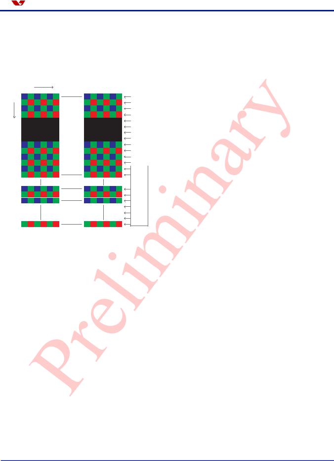
The OV2640 allows the user to define window size or region of interest (ROI), as required by the application. Window size setting (in pixels) ranges from 2 x 4 to 1632 x 1220 (UXGA) or 2 x 2 to 818 x 610 (SVGA), and 408 x 304 (CIF), and can be anywhere inside the 1632 x 1220 boundary. Note that modifying window size or window position does not alter the frame or pixel rate. The windowing control merely alters the assertion of the HREF signal to be consistent with the programmed horizontal and vertical ROI. The default window size is 1600 x 1200. Refer to Figure 4 and registers HREFST, HREFEND, REG32, VSTRT, VEND, and COM1 for details.
Version 1.6, February 28, 2006 |
Proprietary to OmniVision Technologies |
3 |
OV2640 |
Color CMOS UXGA (2.0 MegaPixel) OmniPixel2™ CAMERACHIP™ |
Omni ision |
|
|
|
Figure 4 Windowing
|
Column |
Column |
||
|
Start |
End |
||
|
|
|
||
HREF |
|
|
|
|
|
|
|
|
|
R Column o
w
Row Start
HREF |
Display |
|
|
|
Window |
Row End
Sensor Array
Boundary
Zooming and Panning Mode
The OV2640 provides zooming and panning modes. The user can select this mode under SVGA/CIF mode timing. The related zoom ratios will be 2:1 of UXGA for SVGA and 4:1 of UXGA for CIF. Registers ZOOMS[7:0] (0x49) and COM19[1:0] (0x48) define the vertical line start point. Register ARCOM2[2] (0x34) defines the horizontal start point.
Sub-sampling Mode
The OV2640 supports two sub-sampling modes. Each sub-sampling mode has different resolution and maximum frame rate. These modes are described in the following sections.
SVGA mode
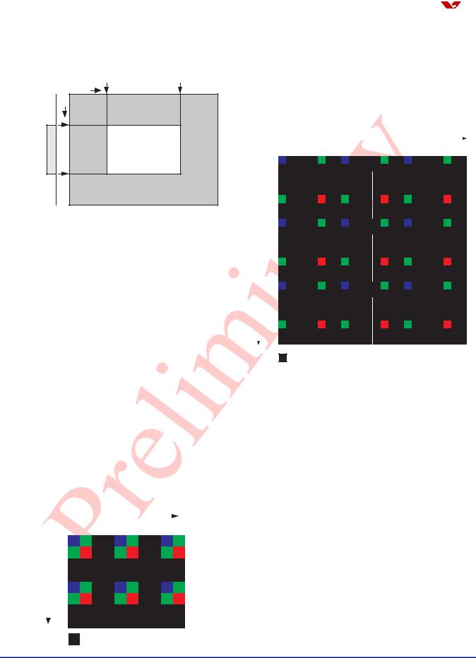
The OV2640 can be programmed to output 800 x 600 (SVGA) sized images for applications where higher resolution image capture is not required. In this mode, both horizontal and vertical pixels will be sub-sampled with an aspect ratio of 4:2 as shown in Figure 5.
Figure 5 SVGA Sub-Sampling Mode
|
Column |
|
|
|
|
|
|
|
|
||
i+2 |
|
|
i+5 |
i+6 |
|
|
|
||||
|
|
i |
i+1 |
i+3 |
i+4 |
i+7 |
i+8 |
i+9 |
|||
Row n |
B |
G |
|
|
B |
G |
|
|
B |
G |
|
|
n+1 |
G |
R |
|
|
G |
R |
|
|
G |
R |
|
n+2 |
|
|
|
|
|
|
|
|
|
|
|
n+3 |
|
|
|
|
|
|
|
|
|
|
|
n+4 |
B |
G |
|
|
B |
G |
|
|
B |
G |
|
n+5 |
G |
R |
|
|
G |
R |
|
|
G |
R |
|
n+6 |
|
|
|
|
|
|
|
|
|
|
|
n+7 |
|
|
|
|
|
|
|
|
|
|
|
|
|
|
|
|
|
|
|
|
|
|
|
|
|
Skipped Pixels |
|
|
|
|
|
|||
|
|
|
|
|
|
|
|
||||
|
|
|
|
|
|
|
|
|
|
|
|
CIF Mode
The OV2640 can also operate at a higher frame rate to output 400 x 296 sized images. Figure 6 shows the sub-sampling diagram in both horizontal and vertical directions for CIF mode.
Figure 6 CIF Sub-Sampling Mode
|
|
Column |
|
|
|
|
|
|
|
|
|
|
|
|
|
|
|
|
|
|
|
|
|
|
|
||
|
|
|
|
|
|
|
|
|
|
i+10 |
i+11 |
i+12 |
i+13 |
i+14 |
i+15 |
i+16 |
i+17 |
i+18 |
i+19 |
i+20 |
i+21 |
i+22 |
i+23 |
||||
|
|
|
i |
i+1 |
i+2 |
i+3 |
i+4 |
i+5 |
i+6 |
i+7 |
i+8 |
i+9 |
|||||||||||||||
Row |
n |
B |
|
|
|
|
G |
|
|
B |
|
|
|
|
G |
|
|
B |
|
|
|
|
G |
|
|
|
|
|
|
|
|
|
|
|
|
|
|
|
|
|
|
|
|
|
|
|
|
|
|||||||
|
|
n+1 |
|
|
|
|
|
|
|
|
|
|
|
|
|
|
|
|
|
|
|
|
|
|
|
|
|
|
|
n+2 |
|
|
|
|
|
|
|
|
|
|
|
|
|
|
|
|
|
|
|
|
|
|
|
|
|
|
|
n+3 |
|
|
|
|
|
|
|
|
|
|
|
|
|
|
|
|
|
|
|
|
|
|
|
|
|
|
|
n+4 |
|
|
|
|
|
|
|
|
|
|
|
|
|
|
|
|
|
|
|
|
|
|
|
|
|
|
|
n+5 |
G |
|
|
|
|
R |
|
|
G |
|
|
|
|
R |
|
|
G |
|
|
|
|
R |
|
|
|
|
|
n+6 |
|
|
|
|
|
|
|
|
|
|
|
|
|
|
|
|
|
|
|
|
|
|
|
|
|
|
|
n+7 |
|
|
|
|
|
|
|
|
|
|
|
|
|
|
|
|
|
|
|
|
|
|
|
|
|
|
|
n+8 |
B |
|
|
|
|
G |
|
|
B |
|
|
|
|
G |
|
|
B |
|
|
|
|
G |
|
|
|
|
|
n+9 |
|
|
|
|
|
|
|
|
|
|
|
|
|
|
|
|
|
|
|
|
|
|
|
|
|
|
n+10 |
|
|
|
|
|
|
|
|
|
|
|
|
|
|
|
|
|
|
|
|
|
|
|
|
|
|
|
n+11 |
|
|
|
|
|
|
|
|
|
|
|
|
|
|
|
|
|
|
|
|
|
|
|
|
|
|
|
n+12 |
|
|
|
|
|
|
|
|
|
|
|
|
|
|
|
|
|
|
|
|
|
|
|
|
|
|
|
n+13 |
G |
|
|
|
|
R |
|
|
G |
|
|
|
|
R |
|
|
G |
|
|
|
|
R |
|
|
|
|
|
n+14 |
|
|
|
|
|
|
|
|
|
|
|
|
|
|
|
|
|
|
|
|
|
|
|
|
|
|
|
n+15 |
|
|
|
|
|
|
|
|
|
|
|
|
|
|
|
|
|
|
|
|
|
|
|
|
|
|
|
n+16 |
B |
|
|
|
|
G |
|
|
B |
|
|
|
|
G |
|
|
B |
|
|
|
|
G |
|
|
|
|
|
n+17 |
|
|
|
|
|
|
|
|
|
|
|
|
|
|
|
|
|
|
|
|
|
|
|
|
|
|
|
n+18 |
|
|
|
|
|
|
|
|
|
|
|
|
|
|
|
|
|
|
|
|
|
|
|
|
|
|
|
n+19 |
|
|
|
|
|
|
|
|
|
|
|
|
|
|
|
|
|
|
|
|
|
|
|
|
|
|
|
n+20 |
|
|
|
|
|
|
|
|
|
|
|
|
|
|
|
|
|
|
|
|
|
|
|
|
|
|
|
n+21 |
G |
|
|
|
|
R |
|
|
G |
|
|
|
|
R |
|
|
G |
|
|
|
|
R |
|
|
|
|
|
n+22 |
|
|
|
|
|
|
|
|
|
|
|
|
|
|
|
|
|
|
|
|
|
|
|
|
|
|
|
n+23 |
|
|
|
|
|
|
|
|
|
|
|
|
|
|
|
|
|
|
|
|
|
|
|
|
|
|
|
|
|
|
Skipped Pixels |
|
|
|
|
|
|
|
|
|
|
|
|
|
|
|
|
|
|
|
||||
|
|
|
|
|
|
|
|
|
|
|
|
|
|
|
|
|
|
|
|
|
|
|
|
|
|
|
|
Timing Generator and Control Logic
In general, the timing generator controls the following:
•Frame Exposure Mode Timing
•Frame Rate Adjust
•Frame Rate Timing
Frame Exposure Mode Timing
The OV2640 supports frame exposure mode. Typically, the frame exposure mode must work with the aid of an external shutter.
The frame exposure pin, FREX (pin B2), is the frame exposure mode enable pin and the EXPST_B pin (pin A2) serves as the sensor's exposure start trigger. When the external master device asserts the FREX pin high, the sensor array is quickly pre-charged and stays in reset mode until the EXPST_B pin goes low (sensor exposure time can be defined as the period between EXPST_B low and shutter close). After the FREX pin is pulled low, the video data stream is then clocked to the output port in a line-by-line manner. After completing one frame of data
4 |
Proprietary to OmniVision Technologies |
Version 1.6, February 28, 2006 |
O |
Functional Description |
mni ision |
output, the OV2640 will output continuous live video data unless in single frame transfer mode. Figure 18 and Figure 19 show the detailed timing and Table 11 shows the timing specifications for this mode.
Output Formatter
This block controls all output and data formatting required prior to sending the image out.
Frame Rate Adjust
The OV2640 offers three methods for frame rate adjustment:
•Clock prescaler: (see “CLKRC” on page 23)
By changing the system clock divide ratio and PLL, the frame rate and pixel rate will change together. This method can be used for dividing the frame/pixel rate by: 1/2, 1/3, 1/4 … 1/64 of the input clock rate.
•Line adjustment: (see “REG2A” on page 26 and “FRARL” on page 26)
By adding a dummy pixel timing in each line (between HSYNC and pixel data out), the frame rate can be changed while leaving the pixel rate as is.
•Vertical sync adjustment:
By adding dummy line periods to the vertical sync period (see “ADDVSL” on page 26 and “ADDVSH” on page 26 or see “FLL” on page 27 and “FLH” on page 27), the frame rate can be altered while the pixel rate remains the same.
Frame Rate Timing
Default frame timing is illustrated in Figure 15, Figure 16, and Figure 17. Refer to Table 1 for the actual pixel rate at different frame rates.
Table 1 Frame/Pixel Rates in UXGA Mode
Frame Rate (fps) |
15 |
7.5 |
2.5 |
1.25 |
|
|
|
|
|
PCLK (MHz) |
36 |
18 |
6 |
3 |
|
|
|
|
|
Digital Signal Processor (DSP)
This block controls the interpolation from Raw data to RGB and some image quality control.
•Edge enhancement (a two-dimensional high pass filter)
•Color space converter (can change Raw data to RGB or YUV/YCbCr)
•RGB matrix to eliminate color cross talk
•Hue and saturation control
•Programmable gamma control
•Transfer 10-bit data to 8-bit
•White pixel canceling
•De-noise
Scaling Image Output
The OV2640 is capable of scaling down the image size from CIF to 40x30. By using SCCB registers, the user can output the desired image size. At certain image sizes, HREF is not consistent in a frame.
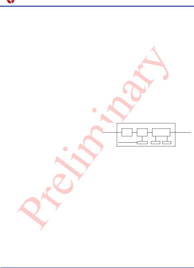
Compression Engine
As shown in Figure 7, the Compression Engine consists of three major blocks:
•DCT
•QZ
•Entropy Encoder
Figure 7 Compression Engine Block Diagram
|
Compression Engine |
|
|
Video Data |
|
|
Compressed |
QZ |
|
Stream |
|
DCT |
Entropy Encoder |
||
Scale Factor |
Q-Table |
H-Table |
Marker |
|
|||
Microcontroller
The OV2640 embeds an 8-bit microcontroller with 512-byte data memory and 4 KB program memory. It provides the flexibility of decoding protocol commands from the host for controlling the system, as well as the ability to fine tune image quality.
SCCB Interface
The Serial Camera Control Bus (SCCB) interface controls the CAMERACHIP operation. Refer to OmniVision Technologies Serial Camera Control Bus (SCCB) Specification for detailed usage of the serial control port.
Slave Operation Mode
The OV2640 can be programmed to operate in slave mode (default is master mode).
When used as a slave device, COM7[3] (0x12), CLKRC[6] (0x11), and COM2[2] (0x09) register bits should be set to
Version 1.6, February 28, 2006 |
Proprietary to OmniVision Technologies |
5 |

OV2640 |
Color CMOS UXGA (2.0 MegaPixel) OmniPixel2™ CAMERACHIP™ |
Omni ision |
|
|
|
"1" and the OV2640 will use PWDN and RESETB pins as vertical and horizontal synchronization triggers supplied by a master device. The master device must provide the following signals:
1.System clock MCLK to XVCLK pin
2.Horizontal sync MHSYNC to RESETB pin
3.Vertical frame sync MVSYNC to PWDN pin
See Figure 8 for slave mode connections and Figure 9 for detailed timing considerations.
Figure 8 Slave Mode Connection
Y[9:0]
RESETB  MHSYNC
PWDN  MVSYNC
XVCLK  MCLK
MCLK
OV2640 |
Master |
|
Device |
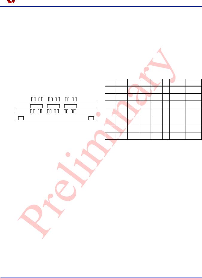
Figure 9 Slave Mode Timing
Tframe
MVSYNC
TVS |
|
|
|
Tline |
|
|
|
|
|
|
|
|
|
|
|
THS |
|
|
|
|
|
|
|
|
|
MHSYNC
Tclk
MCLK
NOTE:
1)THS > 6 Tclk, Tvs > Tline
2)Tline = 1922 x Tclk (UXGA); Tline = 1190 x Tclk (SVGA);
Tline = 595 x Tclk (CIF)
3)Tframe = 1248 x Tline (UXGA); Tframe = 672 x Tline (SVGA); Tframe = 336 x Tline (CIF)
Strobe Mode
The OV2640 has a Strobe mode that allows it to work with an external flash and LED.
Reset
The OV2640 includes a RESETB pin (pin C6) that forces a complete hardware reset when it is pulled low (GND). The OV2640 clears all registers and resets them to their default values when a hardware reset occurs. A reset can also be initiated through the SCCB interface.
Power Down Mode
Two methods are available to place the OV2640 into power-down mode: hardware power-down and SCCB software power-down.
To initiate hardware power-down, the PWDN pin (pin B6) must be tied to high. When this occurs, the OV2640 internal device clock is halted and all internal counters are reset. The current draw is less than 15 µA in this standby mode.
Executing a software power-down through the SCCB interface suspends internal circuit activity but does not halt the device clock. The current requirements drop to less than 1 mA in this mode. All register content is maintained in standby mode.
Digital Video Port
MSB/LSB Swap
The OV2640 has a 10-bit digital video port. The MSB and LSB can be swapped with the control registers. Figure 10 shows some examples of connections with external devices.
Figure 10 Connection Examples
MSB Y9 |
|
|
Y9 |
|
LSB Y9 |
|
|
Y0 |
|
|
|
|
|||||
Y8 |
|
|
Y8 |
|
Y8 |
|
|
Y1 |
|
|
|
|
|||||
Y7 |
|
|
Y7 |
|
Y7 |
|
|
Y2 |
|
|
|
|
|||||
Y6 |
|
|
Y6 |
|
Y6 |
|
|
Y3 |
|
|
|
|
|||||
Y5 |
|
|
Y5 |
|
Y5 |
|
|
Y4 |
|
|
|
|
|||||
Y4 |
|
|
Y4 |
|
Y4 |
|
|
Y5 |
|
|
|
|
|||||
Y3 |
|
|
Y3 |
|
Y3 |
|
|
Y6 |
|
|
|
|
|||||
Y2 |
|
|
Y2 |
|
Y2 |
|
|
Y7 |
|
|
|
|
|||||
Y1 |
|
|
Y1 |
|
Y1 |
|
|
Y8 |
|
|
|
|
|||||
LSB Y0 |
|
|
Y0 |
|
MSB Y0 |
|
|
Y9 |
|
|
|
|
|||||
|
|
|
|
|
|
|
|
|
OV2640 |
|
|
External |
|
OV2640 |
|
|
External |
|
|
|
Device |
|
|
|
|
Device |
Default 10-bit Connection |
|
Swap 10-bit Connection |
||||||
|
|
|
|
|
|
|
|
|
MSB Y9 |
|
|
Y7 |
|
LSB Y9 |
|
|
|
|
|
|
|
|
|
|||
Y8 |
|
|
Y6 |
|
Y8 |
|
|
|
|
|
|
|
|
|
|||
Y7 |
|
|
Y5 |
|
Y7 |
|
|
Y0 |
|
|
|
|
|
||||
Y6 |
|
|
Y4 |
|
Y6 |
|
|
Y1 |
|
|
|
|
|
||||
Y5 |
|
|
Y3 |
|
Y5 |
|
|
Y2 |
|
|
|
|
|
||||
Y4 |
|
|
Y2 |
|
Y4 |
|
|
Y3 |
|
|
|
|
|
||||
Y3 |
|
|
Y1 |
|
Y3 |
|
|
Y4 |
|
|
|
|
|
||||
Y2 |
|
|
Y0 |
|
Y2 |
|
|
Y5 |
|
|
|
|
|
||||
Y1 |
|
|
|
|
Y1 |
|
|
Y6 |
|
|
|
|
|
|
|||
LSB Y0 |
|
|
|
|
MSB Y0 |
|
|
Y7 |
|
|
|
|
|
|
|||
|
|
|
|
|
|
|
|
|
OV2640 |
|
|
External |
|
OV2640 |
|
|
External |
|
|
|
Device |
|
|
|
|
Device |
Default 8-bit Connection |
|
Swap 8-bit Connection |
||||||
6 |
Proprietary to OmniVision Technologies |
Version 1.6, February 28, 2006 |
O |
Functional Description |
mni ision |
Line/Pixel Timing
The OV2640 digital video port can be programmed to work in either master or slave mode.
In both master and slave modes, pixel data output is synchronous with PCLK (or MCLK if port is a slave), HREF, and VSYNC. The default PCLK edge for valid data is the negative edge but may be programmed using register COM10[4] for the positive edge. Basic line/pixel output timing and pixel timing specifications are shown in Figure 14 and Table 10.
Also, using register COM10[5], PCLK output can be gated by the active video period defined by the HREF signal. See Figure 11 for details.
Figure 11 PCLK Output Only at Valid Pixels
PCLK
PCLK active edge negative
HREF
PCLK
PCLK active edge positive
VSYNC
The specifications shown in Table 10 apply for DVDD = +1.2 V, DOVDD = +2.8 V, TA = 25°C, sensor working at 15 fps, external loading = 20 pF.
Pixel Output Pattern
Table 2 shows the output data order from the OV2640. The data output sequence following the first HREF and
after VSYNC is: B0,0 G0,1 B0,2 G0,3… B0,1598 G0,1599. After the second HREF the output is G1,0 R1,1 G1,2 R1,3… G1,1598 R1,1599…, etc. If the OV2640 is programmed to output SVGA resolution data, horizontal and vertical
sub-sampling will occur. The default output sequence for
the first line of output will be: B0,0 G0,1 B0,4 G0,5… B0,1596 G0,1597. The second line of output will be: G1,0 R1,1 G1,4
R1,5… G1,1596 R1,1597.
Table 2 |
Data Pattern |
|
|
|
|||
|
|
|
|
|
|
|
|
R/C |
0 |
1 |
2 |
3 |
. . . |
1598 |
1599 |
0 |
B0,0 |
G0,1 |
B0,2 |
G0,3 |
. . . |
B0,1598 |
G0,1599 |
1 |
G1,0 |
R1,1 |
G1,2 |
R1,3 |
. . . G1,1598 |
R1,1599 |
|
2 |
B2,0 |
G2,1 |
B2,2 |
G2,3 |
. . . |
B2,1598 |
G2,1599 |
3 |
G3,0 |
R3,1 |
G3,2 |
R3,3 |
. . . G3,1598 |
R3,1599 |
|
. |
|
|
|
|
. |
|
|
. |
|
|
|
|
. |
|
|
1198 |
B1198,0 |
G1198,1 B1198,2 G1198,3 |
. . . B1198,1598 |
G1198,1599 |
|||
1199 |
G1199,0 |
R1199,1 |
G1199,2 |
R1199,3 |
. . . G1199,1598 |
R1199,1599 |
|
Version 1.6, February 28, 2006 |
Proprietary to OmniVision Technologies |
7 |

OV2640 |
Color CMOS UXGA (2.0 MegaPixel) OmniPixel2™ CAMERACHIP™ |
Omni ision |
||||||
|
|
|
|
|
|
|
|
|
Pin Description |
|
|
|
|
|
|
||
|
Table 3 |
Pin Description |
|
|
|
|
|
|
|
|
|
|
|
|
|
|
|
|
Pin Location |
Name |
Pin Type |
|
Function/Description |
|
|
|
|
|
|
|
|
|
|
|
|
|
A1 |
|
DOGND |
Ground |
Ground for digital video port |
|
|
|
|
|
|
|
|
|
|
|
|
|
|
|
|
|
Snapshot Exposure Start Trigger |
|
|
|
|
A2 |
|
EXPST_B |
Input |
0: |
Sensor starts exposure (only effective in snapshot mode) |
|
|
|
|
1: |
Sensor stays in reset mode |
|
|
|||
|
|
|
|
|
|
|
||
|
|
|
|
|
Note: There is no internal pull-up/pull-down resistor. |
|
|
|
|
|
|
|
|
|
|
|
|
|
A3 |
|
AGND |
Ground |
Ground for analog circuit |
|
|
|
|
|
|
|
|
|
|
|
|
|
A4 |
|
SGND |
Ground |
Ground for sensor array |
|
|
|
|
|
|
|
|
|
|
||
|
A5 |
|
VREFN |
Reference |
Internal analog reference - connect to ground using a 0.1 µF capacitor |
|
||
|
|
|
|
|
|
|
|
|
|
|
|
|
|
Flash control output |
|
|
|
|
A6 |
|
STROBE |
I/O |
Default: Input |
|
|
|
|
|
|
|
|
Note: There is no internal pull-up/pull-down resistor. |
|
|
|
|
|
|
|
|
|
|
|
|
|
B1 |
|
DOVDD |
Power |
Power for digital video port |
|
|
|
|
|
|
|
|
|
|
|
|
|
B2 |
|
FREX |
Input |
Snapshot trigger - use to activate a snapshot sequence |
|
|
|
|
|
Note: There is no internal pull-up/pull-down resistor. |
|
|
||||
|
|
|
|
|
|
|
||
|
|
|
|
|
|
|
|
|
|
B3 |
|
AVDD |
Power |
Power for analog circuit |
|
|
|
|
|
|
|
|
|
|
|
|
|
B4 |
|
SVDD |
Power |
Power for sensor array |
|
|
|
|
|
|
|
|
|
|
|
|
|
B5 |
|
SVDD |
Power |
Power for sensor array |
|
|
|
|
|
|
|
|
|
|
|
|
|
B6 |
|
PWDN |
Input |
Power-down mode enable, active high |
|
|
|
|
|
Note: There is an internal pull-down resistor. |
|
|
||||
|
|
|
|
|
|
|
||
|
|
|
|
|
|
|
|
|
|
C1 |
|
SIO_D |
I/O |
SCCB serial interface data I/O |
|
|
|
|
|
|
|
|
|
|
|
|
|
C2 |
|
SIO_C |
Input |
SCCB serial interface clock input |
|
|
|
|
|
Note: There is no internal pull-up/pull-down resistor. |
|
|
||||
|
|
|
|
|
|
|
||
|
|
|
|
|
|
|
|
|
|
|
|
|
|
Horizontal reference output |
|
|
|
|
C3 |
|
HREF |
I/O |
Default: Input |
|
|
|
|
|
|
|
|
Note: There is no internal pull-up/pull-down resistor. |
|
|
|
|
|
|
|
|
|
|
|
|
|
C4 |
|
XVCLK |
Input |
System clock input |
|
|
|
|
|
Note: There is no internal pull-up/pull-down resistor. |
|
|
||||
|
|
|
|
|
|
|
||
|
|
|
|
|
|
|
||
|
C5 |
|
VREFH |
Reference |
Internal analog reference - connect to ground using a 0.1 µF capacitor |
|
||
|
|
|
|
|
|
|
|
|
|
C6 |
|
RESETB |
Input |
Reset mode, active low |
|
|
|
|
|
Note: There is an internal pull-up resistor. |
|
|
||||
|
|
|
|
|
|
|
||
|
|
|
|
|
|
|
|
|
|
|
|
|
|
Vertical synchronization output |
|
|
|
|
D2 |
|
VSYNC |
I/O |
Default: Input |
|
|
|
|
|
|
|
|
Note: There is no internal pull-up/pull-down resistor. |
|
|
|
|
|
|
|
|
|
|
|
|
|
D6 |
|
NC |
– |
No connection |
|
|
|
|
|
|
|
|
|
|
|
|
|
|
|
|
|
Video port output bit[1] |
|
|
|
|
E1 |
|
Y1 |
I/O |
Default: Input |
|
|
|
|
|
|
|
|
Note: There is no internal pull-up/pull-down resistor. |
|
|
|
|
|
|
|
|
|
|
|
|
8 |
Proprietary to OmniVision Technologies |
Version 1.6, February 28, 2006 |

O |
|
|
|
Pin Description |
||
mni ision |
|
|
|
|||
|
Table 3 |
Pin Description |
|
|
|
|
|
|
|
|
|
|
|
|
Pin Location |
Name |
Pin Type |
Function/Description |
|
|
|
|
|
|
|
|
|
|
|
|
|
|
Video port output bit[0] |
|
|
E2 |
|
Y0 |
I/O |
Default: Input |
|
|
|
|
|
|
Note: There is no internal pull-up/pull-down resistor. |
|
|
|
|
|
|
|
|
|
|
|
|
|
Pixel clock output |
|
|
E3 |
|
PCLK |
I/O |
Default: Input |
|
|
|
|
|
|
Note: There is no internal pull-up/pull-down resistor. |
|
|
|
|
|
|
|
|
|
E4 |
|
EGND |
Ground |
Ground for internal regulator |
|
|
|
|
|
|
|
|
|
|
|
|
|
Video port output bit[6] |
|
|
E5 |
|
Y6 |
I/O |
Default: Input |
|
|
|
|
|
|
Note: There is no internal pull-up/pull-down resistor. |
|
|
|
|
|
|
|
|
|
E6 |
|
DGND |
Ground |
Ground for digital core |
|
|
|
|
|
|
|
|
|
F1 |
|
EVDD |
Power |
Power for internal regulator |
|
|
|
|
|
|
|
|
|
F2 |
|
DVDD |
Power |
Sensor digital power (Core) |
|
|
|
|
|
|
|
|
|
|
|
|
|
Video port output bit[2] |
|
|
F3 |
|
Y2 |
I/O |
Default: Input |
|
|
|
|
|
|
Note: There is no internal pull-up/pull-down resistor. |
|
|
|
|
|
|
|
|
|
|
|
|
|
Video port output bit[4] |
|
|
F4 |
|
Y4 |
I/O |
Default: Input |
|
|
|
|
|
|
Note: There is no internal pull-up/pull-down resistor. |
|
|
|
|
|
|
|
|
|
|
|
|
|
Video port output bit[8] |
|
|
F5 |
|
Y8 |
I/O |
Default: Input |
|
|
|
|
|
|
Note: There is no internal pull-up/pull-down resistor. |
|
|
|
|
|
|
|
|
|
F6 |
|
DVDD |
Power |
Sensor digital power (Core) |
|
|
|
|
|
|
|
|
|
G1 |
|
EVDD |
Power |
Power for internal regulator |
|
|
|
|
|
|
|
|
|
G2 |
|
DGND |
Ground |
Ground for digital core |
|
|
|
|
|
|
|
|
|
|
|
|
|
Video port output bit[3] |
|
|
G3 |
|
Y3 |
I/O |
Default: Input |
|
|
|
|
|
|
Note: There is no internal pull-up/pull-down resistor. |
|
|
|
|
|
|
|
|
|
|
|
|
|
Video port output bit[5] |
|
|
G4 |
|
Y5 |
I/O |
Default: Input |
|
|
|
|
|
|
Note: There is no internal pull-up/pull-down resistor. |
|
|
|
|
|
|
|
|
|
|
|
|
|
Video port output bit[7] |
|
|
G5 |
|
Y7 |
I/O |
Default: Input |
|
|
|
|
|
|
Note: There is no internal pull-up/pull-down resistor. |
|
|
|
|
|
|
|
|
|
|
|
|
|
Video port output bit[9] |
|
|
G6 |
|
Y9 |
I/O |
Default: Input |
|
|
|
|
|
|
Note: There is no internal pull-up/pull-down resistor. |
|
|
|
|
|
|
|
|
Version 1.6, February 28, 2006 |
Proprietary to OmniVision Technologies |
9 |
OV2640 |
Color CMOS UXGA (2.0 MegaPixel) OmniPixel2™ CAMERACHIP™ |
Omni ision |
|
|
|
Figure 12 Pinout Diagram
A1 |
A2 |
A3 |
A4 |
A5 |
A6 |
DOGND EXPST_B AGND |
SGND VREFN STROBE |
||||
B1 |
B2 |
B3 |
B4 |
B5 |
B6 |
DOVDD |
FREX |
AVDD |
SVDD |
SVDD |
PWDN |
C1 |
C2 |
C3 |
C4 |
C5 |
C6 |
SIO_D SIO_C |
HREF |
XVCLK VREFH RESETB |
|||
|
D2 |
OV2640 |
|
D6 |
|
|
VSYNC |
|
|
|
NC |
E1 |
E2 |
E3 |
E4 |
E5 |
E6 |
Y1 |
Y0 |
PCLK |
EGND |
Y6 |
DGND |
F1 |
F2 |
F3 |
F4 |
F5 |
F6 |
EVDD |
DVDD |
Y2 |
Y4 |
Y8 |
DVDD |
G1 |
G2 |
G3 |
G4 |
G5 |
G6 |
EVDD |
DGND |
Y3 |
Y5 |
Y7 |
Y9 |
Table 4 |
Ball Matrix |
|
|
|
|
|
|
|
|
|
|
|
|
|
1 |
2 |
3 |
4 |
5 |
6 |
|
|
|
|
|
|
|
A |
DOGND |
EXPST_B |
AGND |
SGND |
VREFN |
STROBE |
|
|
|
|
|
|
|
B |
DOVDD |
FREX |
AVDD |
SVDD |
SVDD |
PWDN |
|
|
|
|
|
|
|
C |
SIO_D |
SIO_C |
HREF |
XVCLK |
VREFN |
RESETB |
|
|
|
|
|
|
|
D |
|
VSYNC |
|
|
|
NC |
|
|
|
|
|
|
|
E |
Y1 |
Y0 |
PCLK |
EGND |
Y6 |
DGND |
|
|
|
|
|
|
|
F |
EVDD |
DVDD |
Y2 |
Y4 |
Y8 |
DVDD |
|
|
|
|
|
|
|
G |
EVDD |
DGND |
Y3 |
75 |
Y7 |
Y9 |
|
|
|
|
|
|
|
10 |
Proprietary to OmniVision Technologies |
Version 1.6, February 28, 2006 |
O |
Electrical Characteristics |
mni ision |
Electrical Characteristics
Table 5 |
Absolute Maximum Ratings |
|
|
|
|
|
|
Ambient Storage Temperature |
|
-40ºC to +95ºC |
|
|
|
|
|
|
|
VDD-A |
4.5V |
Supply Voltages (with respect to Ground) |
VDD-C |
3V |
|
|
|
VDD-IO |
4.5V |
All Input/Output Voltages (with respect to Ground) |
|
-0.3V to VDD-IO+1V |
|
Lead-free Temperature, Surface-mount process |
|
245ºC |
|
|
|
|
|
ESD Rating, Human Body model |
|
2000V |
|
|
|
|
|
NOTE: Exceeding the Absolute Maximum ratings shown above invalidates all AC and DC electrical specifications and may result in permanent device damage.
Table 6 |
DC Characteristics (-30°C < TA < 70°C) |
|
|
|
|
Symbol |
Parameter |
Min |
Typ |
Max |
Unit |
Supply |
|
|
|
|
|
VDD-A |
Supply voltage |
2.5 |
2.8 |
3.0 |
V |
VDD-D |
Supply voltage |
1.14 |
1.2 |
1.26 |
V |
VDD-IO |
Supply voltagea |
1.71 |
2.8 |
3.3 |
V |
I |
Active (Operating) Currentb |
|
30 |
40 |
mA |
DDA-A |
|
|
|
|
|
I |
Active (Operating) Currentb |
|
25 (YUV) |
35 (YUV) |
mA |
DDA-D |
|
|
35 (Compressed) |
50 (Compressed) |
|
I |
Active (Operating) Currentb |
|
6 |
10 |
mA |
DDA-IO |
|
|
|
|
|
IDDS-SCCB |
Standby Currentb |
|
1 |
2 |
mA |
IDDS-PWDN |
|
600 |
1200 |
µA |
|
|
|
||||
Digital Inputs
VIL |
Input voltage LOW |
|
|
0.54 |
V |
VIH |
Input voltage HIGH |
1.26 |
|
|
V |
CIN |
Input capacitor |
|
|
10 |
pF |
Digital Outputs (standard loading 25 pF) |
|
|
|
|
|
|
|
|
|
|
|
VOH |
Output voltage HIGH |
1.62 |
|
|
V |
VOL |
Output voltage LOW |
|
|
0.18 |
V |
Serial Interface Inputs |
|
|
|
|
|
|
|
|
|
|
|
VIL |
SIO_C and SIO_D |
-0.5 |
0 |
0.54 |
V |
VIH |
SIO_C and SIO_D |
1.26 |
1.8 |
2.3 |
V |
a.1.8V I/O is supported. Contact your local OmniVision FAE for further details.
b.VDD-A = 2.8V, VDD-D = 1.2V, and VDD-IO = 1.8V for 15 fps in UXGA mode
IDDS-SCCB refers to SCCB-initiated Standby, while IDDS-PWDN refers to PWDN pad-initiated Standby
Version 1.6, February 28, 2006 |
Proprietary to OmniVision Technologies |
11 |

OV2640 |
Color CMOS UXGA (2.0 MegaPixel) OmniPixel2™ CAMERACHIP™ |
|
Omni ision |
|||||||||
|
|
|
|
|
|
|
|
|
|
|
|
|
|
Table 7 |
AC Characteristics (TA = 25°C, VDD-A = 2.8V) |
|
|
|
|
|
|
|
|
||
|
|
|
|
|
|
|
|
|
|
|
|
|
|
Symbol |
|
Parameter |
Min |
Typ |
Max |
|
Unit |
||||
|
|
|
|
|
|
|
|
|
|
|
|
|
|
ADC Parameters |
|
|
|
|
|
|
|
|
|||
|
|
|
|
|
|
|
|
|
|
|
|
|
|
B |
|
Analog bandwidth |
|
|
20 |
|
|
|
MHz |
||
|
|
|
|
|
|
|
|
|
|
|
|
|
|
DLE |
|
DC differential linearity error |
|
|
0.5 |
|
|
|
LSB |
||
|
|
|
|
|
|
|
|
|
|
|
|
|
|
ILE |
|
DC integral linearity error |
|
|
1 |
|
|
|
LSB |
||
|
|
|
|
|
|
|
|
|
|
|
|
|
|
|
|
Settling time for hardware reset |
|
|
|
|
<1 |
|
ms |
||
|
|
|
|
|
|
|
|
|
|
|
|
|
|
|
|
Settling time for software reset |
|
|
|
|
<1 |
|
ms |
||
|
|
|
|
|
|
|
|
|
|
|
|
|
|
|
|
Settling time for UXGA/SVGA mode change |
|
|
|
|
<1 |
|
ms |
||
|
|
|
|
|
|
|
|
|
|
|
|
|
|
|
|
Settling time for register setting |
|
|
|
|
<300 |
|
ms |
||
|
|
|
|
|
|
|
|
|
|
|
|
|
|
Table 8 |
Timing Characteristics |
|
|
|
|
|
|
|
|
||
|
|
|
|
|
|
|
|
|
|
|
|
|
|
Symbol |
|
Parameter |
|
Min |
|
Typ |
|
Max |
|
Unit |
|
|
|
|
|
|
|
|
|
|
|
|
|
|
|
Oscillator and Clock Input |
|
|
|
|
|
|
|
|
|||
|
|
|
|
|
|
|
|
|
|
|
|
|
|
fOSC |
|
Frequency (XVCLK) |
|
6 |
|
24 |
|
|
|
MHz |
|
|
tr, tf |
|
Clock input rise/fall time |
|
|
|
|
|
5 |
|
ns |
|
|
|
|
Clock input duty cycle |
|
45 |
|
50 |
|
55 |
|
% |
|
|
|
|
|
|
|
|
|
|
|
|
|
|
12 |
Proprietary to OmniVision Technologies |
Version 1.6, February 28, 2006 |
O |
Timing Specifications |
mni ision |
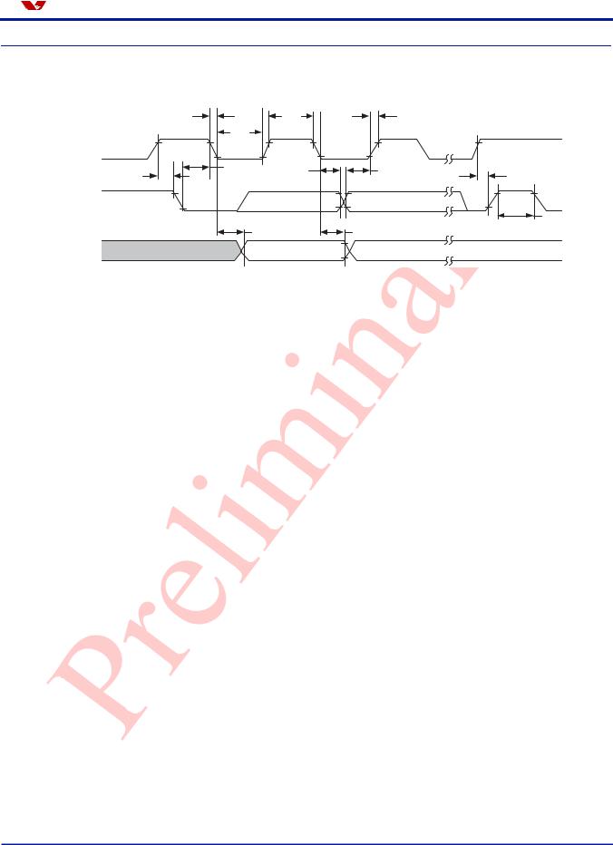
Timing Specifications
Figure 13 SCCB Interface Timing Diagram
tF |
|
t |
HIGH |
t |
R |
|
|
tLOW |
|
|
|
|
|
SIOC |
|
|
|
|
|
|
tSU:STA |
tHD:STA |
tHD:DAT |
tSU:DAT |
t |
||
|
|
|
|
|
|
SU:STO |
SIOD IN |
|
|
|
|
|
|
|
|
|
|
|
|
tBUF |
|
|
tAA |
|
tDH |
|
|
SIOD OUT
Table 9 |
SCCB InterfaceTiming Specifications |
|
|
|
|
|
|
|
|
|
|
Symbol |
Parameter |
Min |
Typ |
Max |
Unit |
|
|
|
|
|
|
fSIO_C |
Clock Frequency |
|
|
400 |
KHz |
tLOW |
Clock Low Period |
1.3 |
|
|
µs |
tHIGH |
Clock High Period |
600 |
|
|
ns |
tAA |
SIOC low to Data Out valid |
100 |
|
900 |
ns |
tBUF |
Bus free time before new START |
1.3 |
|
|
µs |
tHD:STA |
START condition Hold time |
600 |
|
|
ns |
tSU:STA |
START condition Setup time |
600 |
|
|
ns |
tHD:DAT |
Data-in Hold time |
0 |
|
|
µs |
tSU:DAT |
Data-in Setup time |
100 |
|
|
ns |
tSU:STO |
STOP condition Setup time |
600 |
|
|
ns |
tR, tF |
SCCB Rise/Fall times |
|
|
300 |
ns |
tDH |
Data-out Hold time |
50 |
|
|
ns |
Version 1.6, February 28, 2006 |
Proprietary to OmniVision Technologies |
13 |
Loading...