

OMNIREL OMS410, OMS510, OMS410A Datasheet

OMS510
OMS410AOMS410
3 PHASE, LO W VOLTA GE, LO W R
DS(on)
, MOSFET
BRIDGE CIRCUIT IN A PLASTIC PA CKA GE
Three Phase, 100 Volt, 15 To 45 Amp Bridge
With Current And Temperature Sensing
In A Low Profile Package
FEATURES
• Three Phase Power Switch Configuration
• Zener Gate Protection
• 10 Miliohm Shunt Resistor
• Linear Thermal Sensor
• Isolated Low Profile Package
• Output Currents Up To 45 Amps
DESCRIPTION
This series of MOSFET switches is configured in a 3 phase bridge with a common
VDDline, precision series shunt resistor in the source line, and a sensing element to
monitor the substrate temperature. This device is ideally suited for Motor Control
applications where size, performance, and efficiency are key.
2.1
DS
(@ 25°C)
R
DS(on)
I
D
Package
MAXIMUM RATINGS
Part V
Number (Volts) (m ) (Amps)
OMS410 100 85 15 MP-3
OMS410A 100 85 20 MP-3
OMS510 100 42 45 MP-3
SCHEMATIC
21 65 109
32, 33, 34
21
22
34 78 1112 13 14
29, 30, 31
26, 27, 28
23, 24, 25
1 5, 16, 17
18, 19, 20
4 11 R0
2.1 - 53
OMS410, OMS410A, OMS510
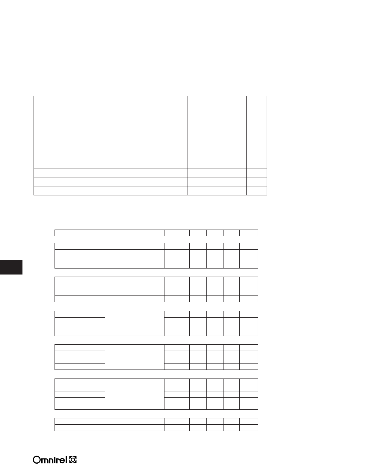
ABSOLUTE MAXIMUM RATINGS (TC= 25°C unless otherwise noted)
Parameter OMS410 OMS410A OMS510 Units
V
DS
V
DGR
ID@ TC= 25°C Continuous Drain Current 15 20 45 A
ID@ TC= 70°C Continuous Drain Current 11 16 45 A
I
DM
PD@ TC= 25°C Maximum Power Dissipation
PD@ TC= 70°C Maximum Power Dissipation
Junction-To-Case Linear Derating Factor 0.33 0.33 0.66 W/°C
Thermal Resistance Junction-To-Case 3.0 3.0 1.5 °C/W
Sense Resistor 0.010 0.010 0.010 Ohms
Note 1: Pulse Test: Pulse width 300 sec. Duty Cycle 1.5%.
Note 2: Maximum Junction Temperature equal to 125°C.
Drain-Source Voltage 100 100 100 V
Drain-Gate Voltage (RGS= 1 m ) 100 100 100 V
Pulsed Drain Current
1
2
2
110 110 180 A
33 33 66 W
18 18 36 W
2.1
ELECTRICAL CHARACTERISTICS: OMS410
(TC= 25° unless otherwise specified)
Characteristic Test Conditions Symbol Min. Typ. Max. Unit
OFF CHARACTERISTICS
Drain-Source Breakdown Voltage, ID= 250 µA, VGS= 0 V
Zero Gate Voltage Drain Current = V
Gate-Body Leakage, V
= ±12 V I
GS
, VDS= Max. Rat. I
GS
V
= Max. Rat. x 0.8, TC= 70°C - - 100 µA
DS
ON CHARACTERISTICS
Gate-Threshold Voltage, VDS= VGS, ID= 250 µA V
Static Drain-Source On-Resistance, V
Static Drain-Source On-Resistance T
On State Drain Current, V
DS
= 10 Vdc, ID= 9.0 A R
GS
= 70°C - - 0.1
C
> I
X R
D(on)
Max., VGS= 10 I
DS(on)
DYNAMIC CHARACTERISTICS
Forward Transconductance VDS> I
Input Capacitance V
Output Capacitance V
Reverse Transfer Capacitance f = 1.0 mHz C
D(on)
X R
Max., ID= 9.0 A, g
DS(on)
DS
= 25 V, C
= 0, C
GS
SWITCHING CHARACTERISTICS
Turn-On Delay Time t
Rise Time V
Turn-Off Delay Time R
= 100 V, ID= 15 A, t
DD
= 10 , VGS= 10 V t
GS
Fall Time t
SOURCE DRAIN DIODE CHARACTERISTICS
Source - Drain Current I
Source - Drain Current (Pulsed) I
Forward On-Voltage I
Reverse Recovery Time I
SD
= 28 A, VGS= 0, V
SD
= 13 A, di/dt = 100 A/µSec t
Reverse Recovered Charge Q
RESISTOR CHARACTERISTICS
Resistor Tolerance R
Temperature Coefficient, -40°C to +70°C T
* Indicates Pulse Test 300 µsec, Duty Cycle 1.5%
BRDSS
DSS
GSS
GSth
DSon
Don
fs
iss
oss
rss
don
r
doff
f
SD
SDM
SD
rr
S
cr
100 - - V
- - 10 µA
- - ±500 nA
2.0 - 4.0 V
- - 0.058
15--A
9.0 - - mho
- - 2600 pF
- - 910 pF
- - 350 pF
- - 35 ns
- - 290 ns
- - 85 ns
- - 120 ns
--14A
*--56A
- - 2.5 V
- 133 - ns
rr
- 0.85 - µC
9.0 10 11 m
- 100 - ppm
2.1 - 54
 Loading...