

3.3 - 1
3.3
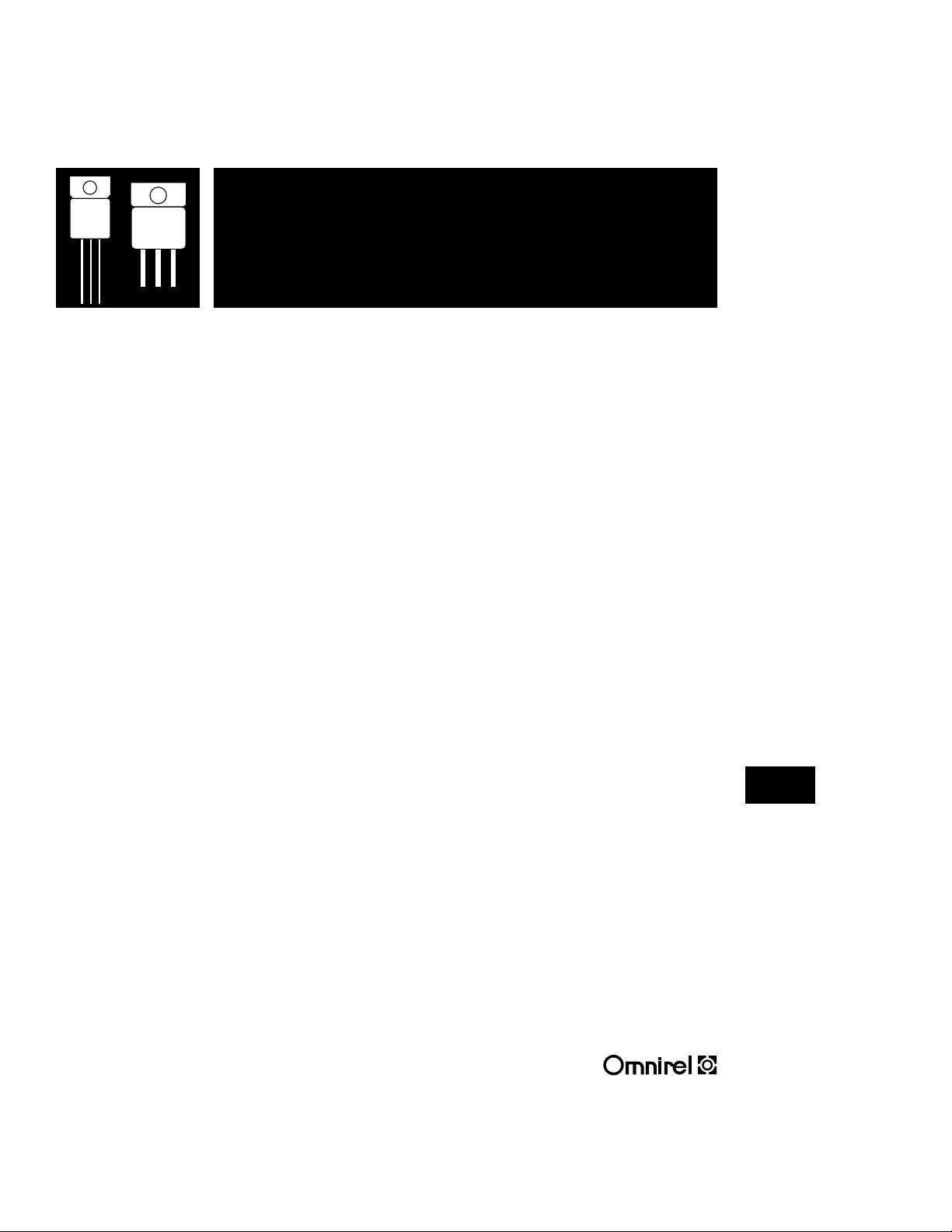
Three Terminal Adjustable Low Dropout
TO-257/TO-258 Positive Voltage Regulators
0 03 R3
Supersedes 4 11 R2
7.5A, 5A, 3A, 1.5A LOW DROPOUT POSITIVE
ADJUSTABLE REGULATORS
FEATURES
• Operates Down to 1V Dropout, 1.5V @ Max. Current
• .015% Line Regulation
• .01% Load Regulation
• 1% Reference Voltage
• Hermetic TO-257 and TO-258 Isolated Packages
• Electrically Equivalent to LT1083, 84, 85 and 86
DESCRIPTION
These three terminal positive adjustable voltage regulators are designed to provide
7.5A, 5A, 3A, and 1.5A with higher efficiency than conventional v oltage regulators. The
devices are designed to operate to 1 Volt input to output differential and the dropout
voltage is specified as a function of load current. All devices are pin compatible with
older three terminal regulators. Supplied in the easy-to-use hermetic metal TO-257
and TO-258 JEDEC packages also supplied in Omnirel’s new surface mount D2Pac..
These devices are ideally suited for Military applications where small size, hermeticity
and high reliability are required.
ABSOLUTE MAXIMUM RATINGS @ 25°C
Input Voltage . . . . . . . . . . . . . . . . . . . . . . . . ............................ 35 V
Operating Junction Temperature Range . ................... - 55°C to + 150°C
Storage Temperature . ............................. - 65°C to + 150°C
Output Current - OM183SC . ....................................... 7.5 A
OM184SC . ........................................ 5 A
OM185ST/SR. ....................................... 3 A
OM186ST/SR . ....................................... 1.5 A
Note: OM183SC and OM184SC products are packaged in the TO-258 Package (7.5A & 5A).
OM185ST and OM186ST products are packaged in the TO-257 Package (3A & 1.5A).
OM185ST
OM186ST
OM183SC
OM184SC
OM185SR
OM186SR
3.3 - 2
3.3
OM183SC - OM186ST - OM186SR
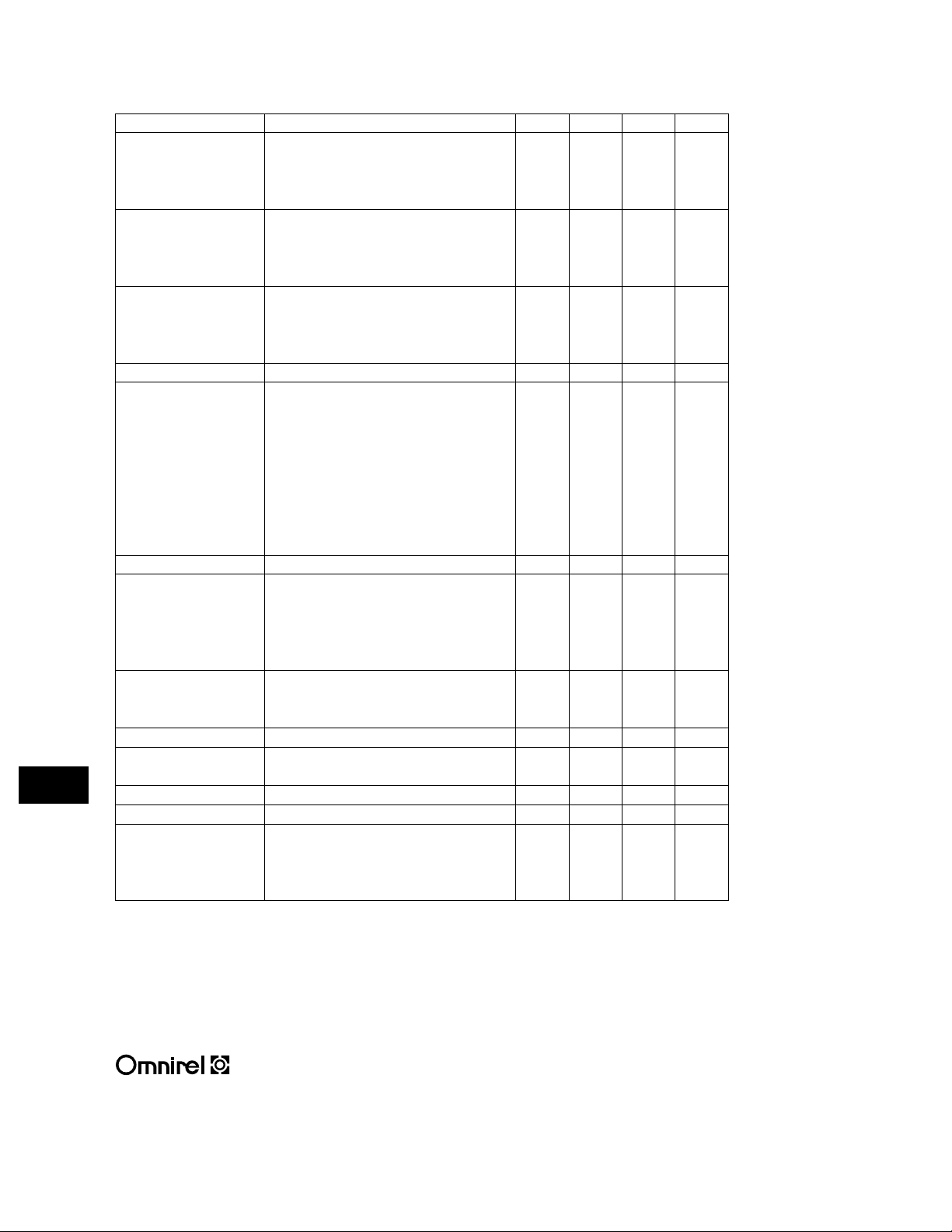
ELECTRICAL CHARACTERISTICS (T
C
= 25°C unless otherwise noted)
Parameter Conditions Min. Typ. Max. Units
Reference V oltage I
OUT
= 10 mA, Tj= 25°C
(V
IN
- V
OUT
) = 3 V 1.238 1.250 1.262 V
10mA ≤ I
OUT
≤ I
FULL LOAD
1.5 V ≤ (VIN- V
OUT
) ≤ 25 V (Note 3) 1.220 1.250 1.270 V
Line Regulation I
LOAD
= 10 mA, 1.5 V ≤ (VIN- V
OUT
) ≤ 15 V, 0.015 0.2 %
T
j
= 25°C 0.035 0.2 %
15 V ≤ (V
IN
- V
OUT
) ≤ 35 V (Notes 1 & 2) 0.05 0.5 %
Load Regulation (V
IN
- V
OUT
) = 3 V
10 mA ≤ I
OUT
≤ I
FULL LOAD
Tj= 25°C 0.5 0.8 %
(Notes 1, 2, 3) .8 1.0 %
Dropout Voltage ∆V
REF
=
1%, I
OUT
= I
FULL LOAD
1.3 1.5 V
Current Limit
OM183SC (V
IN
- V
OUT
) = 5 V 8.0 A
(V
IN
- V
OUT
) = 25 V 0.4 A
OM184SC (V
IN
- V
OUT
) = 5 V 5.5 A
(V
IN
- V
OUT
) = 25 V 0.3 A
OM185ST/SR (V
IN
- V
OUT
) = 5 V 3.2 A
(V
IN
- V
OUT
) = 25 V 0.2 A
OM186ST/SR (V
IN
- V
OUT
) = 5 V 1.5 A
(V
IN
- V
OUT
) = 25 V 0.75 A
Minimum Load Current (V
IN
- V
OUT
) = 25 V 5 10 mA
Thermal Regulation T
A
= 25°C, 30 ms pulse
OM183SC Guaranteed by design 0.002 0.01 %/W
OM184SC 0.003 0.15 %/W
OM185ST/SR 0.004 0.02 %/W
OM186ST/SR 0.010 0.05 %/W
Ripple Rejection f = 120 Hz
C
ADJ
= 25 µF Tantalum
I
OUT
- I
FULL LOAD (VIN
- V
OUT
) = 3 V 60 75 dB
Adjust Pin Current T
J
= 25°C 55 µA
Adjust Pin Current Change 10mA ≤ I
OUT
≤ I
FULL LOAD
1.5 V ≤ (VIN- V
OUT
) ≤ 25 V 0.2 5 µA
Temperature Stability -55°C ≤ T
J
≤ +150°C 0.5 %
Long T erm Stability T
A
= 125°C, 1000 Hrs. 0.3 1 %
Thermal Resistance Junction-to-Case
TO-257AA/D
2
Pac 4.2 °C/W
TO-258AA 2.75 °C/W
Note 1: Load and line regulation are measured at a constant junction temperature by low duty cycle pulse testing.
Note 2: Line and load regulation are guaranteed up to the maximum power dissipation (OM183/60W, OM184/45W, OM185/30W,
OM186/15W). Power dissipation is determined by the input/output differential and the output current. Guaranteed maximum
power dissipation will not be available over the full input/output voltage range.
Note 3: I
FULL LOAD
curve is defined as the minimum value of current limit as a function of input to output voltage. Note that power
dissipation is only achievable over a limited range of input to output voltage.
Note 4: Dropout voltage is specified over the full output current range of the device.

3.3 - 3
3.3
OM183SC - OM186ST - OM186SR
TYPICAL PERFORMANCE CHARACTERISTICS
Minimum Input/Output Differential (V)
2
1
0
012345678910
Output Current (A)
OM183SC Dropout Voltage
TJ = 25°C
Output Voltage Deviation (%)
0.10
0.05
0
-0.05
-0.10
-0.15
-0.20
-50 -25 0 25 50 75 100 125 150
Temperature (°C)
OM183SC Load Regulation
I = 7.5A
Output Voltage Deviation (%)
0.10
0.05
0
-0.05
-0.10
-0.15
-0.20
-50 -25 0 25 50 75 100 125 150
Temperature (°C)
OM184SC Load Regulation
I = 5A
Minimum Input/Output Differential (V)
2
1
0
012
Output Current (A)
OM186ST Dropout Voltage
TJ = 25°C
Output Voltage Deviation (%)
0.10
0.05
0
-0.05
-0.10
-0.15
-0.20
-50 -25 0 25 50 75 100 125 150
Temperature (°C)
OM185ST Load Regulation
I = 3A
Minimum Input/Output Differential (V)
2
1
0
0123456
Output Current (A)
OM184SC Dropout Voltage
TJ = 25°C
Minimum Input/Output Differential (V)
2
1
0
01234
Output Current (A)
OM185ST Dropout Voltage
TJ = 25°C
Short Circuit Current (A)
12
10
8
6
4
2
0
50 101520253035
Input/Output Differential (V)
OM183SC Short Circuit Current
TJ = 150°C
TJ = -55°C
I
FULL LOAD
TJ = 25°C
Short Circuit Current (A)
10
9
8
6
6
5
4
3
2
1
0
50 10 15 20 25 30 35
Input/Output Differential (V)
OM184SC Short Circuit Current
TJ = 25°C
TJ = -55°C
I
FULL LOAD
TJ = 150°C
Short Circuit Current (A)
6
5
4
3
2
1
0
50 10 15 20 25 30 35
Input/Output Differential (V)
OM185ST Short Circuit Current
TJ = 25°C
TJ = -55°C
I
FULL LOAD
TJ = 150°C
0.10
0.05
0
-0.05
-0.10
-0.15
-0.20
-50 -25 0 25 50 75 100 125 150
Temperature (°C)
OM186ST Load Regulation
I = 3A
Output Voltage Deviation (%)
Short Circuit Current (A)
3.0
2.5
2.0
1.5
1
.5
0
50 10 15 20 25 30 35
Input/Output Differential (V)
OM186ST Short Circuit Current
TJ = 25°C
TJ = -55°C
I
FULL LOAD
TJ = 150°C

3.3
205 Crawford Street, Leominster, MA 01453 USA (508) 534-5776 FAX (508) 537-4246
OM183SC - OM186ST - OM186SR
Pin 1 - Adjust
Pin 2 - V
OUT
Pin 3 - V
IN
123
Pin 1 - Adjust
Pin 2 - V
OUT
Pin 3 - V
IN
123
MECHANICAL SPECIFICATIONS
P/N OM183SC and OM184SC JEDEC TO-258AA
P/N OM185ST and OM186ST JEDEC TO-257AA
Stability
The OM183-186 Series requires the use of an output
capacitor as part of the device frequency compensation.
For all operating conditions, the addition of 150µF aluminum electrolytic or a 22µF solid tantalum on the output
will ensure stability. Normally, capacitors much smaller
than this can be used. Many different types of capacitors
with widely varying characteristics are available. These
capacitors differ in capacitor tolerance (sometimes ranging
up to ±100%), equivalent series resistance, and capacitance temperature coefficient.
The 150µF or 22µF values given will ensure stability.
When the adjustment terminal is bypassed to improve the
ripple rejection, the requirement for an output capacitor
increases. The values of 22µF tantalum or 150µF aluminum cover all cases of bypassing the adjustment terminal. Without bypassing the adjustment terminal, smaller
capacitors can be used with equally good results and the
table below shows approximately what size capacitors are
needed to ensure stability.
Recommended Capacitor Values
Normally, capacitor v alues on the order of 100µF are used
in the output of many regulators to ensure good transient
response with heavy load current changes. Output capacitance can be increased without limit and larger values of
output capacitor further improve stability and transient
response of the OM183SC regulators.
Output Voltage — Adjustable Regulators
The OM183-OM186 devices develop a 1.25V reference
voltage between the output and the adjust terminal (see
below). By placing a resistor, R1, between these two terminals, a constant current is caused to flow through R1
and down through R2 to set the overall output voltage.
Normally this current is the specified minimum load current
of 10mA. Because I
ADJ
is very small and constant when
compared with the current through R1, it represents a
small error and can usually be ignored.
Basic Adjustable Regulator
APPLICATION NOTES
Input Output Adjustment
10µF 10µF Tantalum, 50µF Aluminum None
10µF 22µF Tantalum, 150µF Aluminum 20µF
.165
.155
.707
.697
.750
.500
.200 TYP.
.695
.685
.835
.815
V
IN
.270
.240
.045
.035
.550
.530
.092 MAX.
.065
.055
.140 TYP.
.005
V
OUT
IN OUTOM183SC
I
50 µA
R2
= V
(1 + ) + I
REF
ADJ
R1
V
ADJ
ADJ
R2
OUT
V
R1
REF
R2
.150
.140
.200
.430
.410
.190
.045
.035
.038 MAX.
.005
.120 TYP.
.420
.410
.665
.645
.537
.527
.750
.500
.035
.025
.100 TYP.

OM183SC - OM186ST - OM186SR
OM 183 S R M
Omnirel Device Isolated Package Hi-Rel Screening
Type Package Style Level
PART NUMBER DESIGNATOR
Figure 1 shows a typical soldering profile for the D2and D3Packages when soldering a to a printed circuit board.The
profile will vary from system to system and solders to solders. Factors that can affect the profile include the type of soldering system used, density and type of components on the board or substrate material being used.This profile shows
temperature versus time.The two profiles described are based on a high density and a low density board.The type solder used was 62/36/2 Tin Lead Silver with a melting point between 177-189ºC.An convection/infrared soldering reflow
system was used.The circuit and solder joints heat up first due to their mass followed by the components which typically run 30 degrees cooler than the solder joints.
TYPICAL HEATING PROFILE
TYPICAL SOLDERING PROFILE
MECHANICAL OUTLINE SOLDERING FOOTPRINT
Pin 1: Adjust
Pin 2: Vout
Pin 3: Vin
Case N/C
205 Crawford Street, Leominster, MA 01453 USA (508) 534-5776 FAX (508) 537-4246
123
 Loading...