

OMNIREL OM185SR, OM185SM, OM186SR, OM186SM, OM185NR Datasheet
...
3.5 - 43
3.5
Three Terminal, Adjustable Low Dropout
2.0 Amp And 1.0 Amp Positive
Voltage Regulators
4 11 R0
SURFACE MOUNT LOW DROPOUT POSITIVE
ADJUSTABLE REGULATOR
FEATURES
• Hermetic Surface Mount Package
• Operates Down To 1V Dropout, 1.5V @ Max. Current
• .020% Line Regulation Typically
• .050% Load Regulation Typically
• 1% Reference Voltage
• Electrically Equivalent To LT1085 And LT1086
• Available Hi-Rel Screened
DESCRIPTION
These three terminal positive adjustable voltage regulators in a surface mount
package are designed to provide 2.0 Amps and 1.0 Amp with higher efficiency than
conventional voltage regulators. The devices are designed to operate to 1 Volt input
to output differential and the dropout voltage is specified as a function of load current.
These devices are ideally suited for Hi-Rel applications where surface mount, small
size, hermeticity and high reliability are required.
ABSOLUTE MAXIMUM RATINGS@ 25°C
Input Voltage ...........................................................35 V
Operating Junction Temperature Range ........................- 55°C to + 150°C
Storage Temperature Range ..................................- 55°C to + 150°C
Output Current - OM185SM..........................................2.0 A
Output Current - OM186SM..........................................1.0 A
Thermal Resistance - OM185SM ........................................9°C/W
Thermal Resistance - OM186SM .......................................14°C/W
Lead Temperature (Soldering 10 Seconds)................................280°C
OM185SM/SR/NR
OM186SM/SR/NR
3.5 - 44
OM185SM/SR/N R - OM186SM/SR/NR
3.5
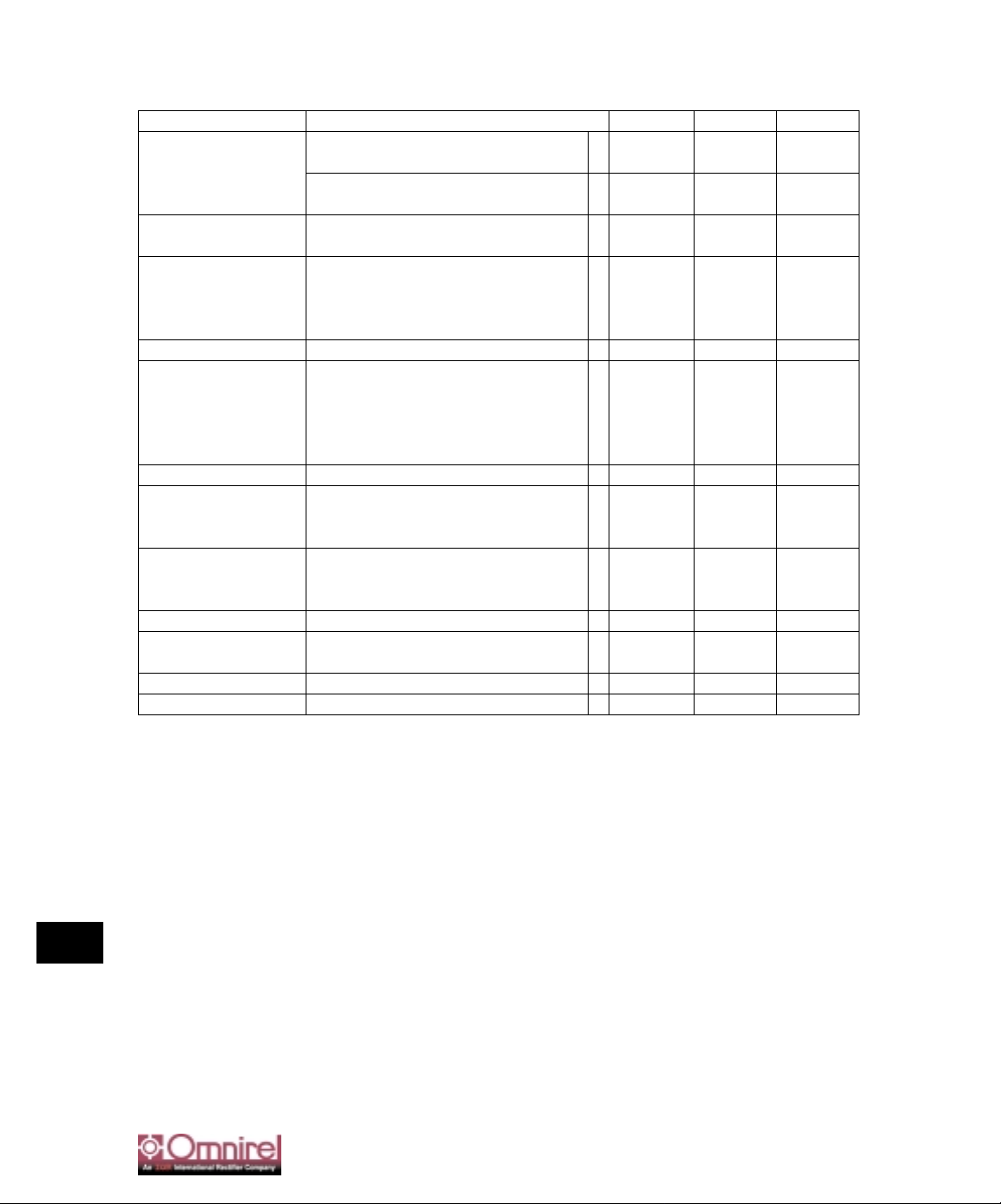
ELECTRICAL CHARACTERISTICS (T
J
= -55°C to +125°C)
Parameter Conditions Min. Max. Units
Reference Voltage I
OUT
= 10mA, Tj= 25°C
(VIN- V
OUT
) = 3V 1.238 1.262 V
10mA ≤ I
OUT≤IFULL LOAD
1.5V ≤ (VIN- V
OUT
) ≤ 25 V (Note 3) • 1.220 1.270 V
Line Regulation I
LOAD
= 10mA, 1 .5V ≤(VIN-V
OUT
) ≤ 15V, Tj= 25°C 0.25 %
15V ≤ (VIN- V
OUT
) ≤ 35V (Notes 1 & 2) • 0.6 %
Load Regulation (VIN- V
OUT
) = 3V
10mA ≤ I
OUT≤IFULL LOAD
Tj= 25°C (Notes 1, 2, & 3) 1.0 %
• 1.2 %
Dropout Voltage ∆V
REF
= 1%, I
OUT
= I
FULL LOAD
• 1.5 V
Current Limit
OM185SM (VIN- V
OUT
) = 5V • 2.0 A
(VIN- V
OUT
) = 25V • 0.10 A
OM186SM (VIN- V
OUT
) = 5V • 1.0 A
(VIN- V
OUT
) = 25V • 0.05 A
Minimum Load Current (VIN- V
OUT
) = 25V • 15 mA
Thermal Regulation TA= 25°C, 30 ms pulse
OM185SM 0.025 %/W
OM186SM 0.055 %/W
Ripple Rejection f = 120Hz
C
ADJ
= 25µF Tantalum
I
OUT
- I
FULL LOAD (VIN
- V
OUT
) = 3V 60 dB
Adjust Pin Current TJ= 25°C 120 µA
Adjust Pin Current Change 10mA ≤ I
OUT≤IFULL LOAD
1.5V ≤ (VIN- V
OUT
) ≤ 25V • 5 µA
Temperature Stability -55°C ≤ TJ≤ +150°C 1 %
Long Term Stability TA= 125°C, 1000 Hrs. 1 %
Note 1: Load and line regulation are measured at a constant junction temperature by low duty cycle pulse testing.
Note 2: Line and load regulation are guaranteed up to the maximum power dissipation (OM185/20W, OM186/10W).
Power dissipation is determined by the input/output differential and the output current. Guaranteed maximum
power dissipation will not be available over the full input/output voltage range.
Note 3: I
FULL LOAD
curve is defined as the minimum value of current limit as a function of input to output voltage. Note that
power dissipation is only achievable over a limited range of input to output voltage.
Note 4: Dropout voltage is specified over the full output current range of the device.
The •denotes the specifications which apply over the full operating temperature range.
 Loading...