


COM7905T
COM7912T
(COTS) COMMERCIAL OFF-THE-SHELF FIXED
VOLTAGE NEGATIVE REGULATORS IN TO-257
Three Terminal, Fixed Voltage, 1.5 Amp
Precision Negative Regulators In Hermetic
JEDEC TO-257AA Package
FEATURES
• Isolated Hermetic Package, JEDEC TO-257AA Outline
• Output Voltages: -5V, -12V, -15V
• Output Voltages Set Internally To ± 2%
• Built-In Thermal Overload Protection
• Short Circuit Current Limiting
• Standard Off-The-Shelf
COM7915T
DESCRIPTION
These three terminal negative regulators are supplied in a hermetically sealed
metal package whose outline is similar to the industry standard T O-220 plastic
package. All protective features are designed into the circuit, including thermal
shutdown, current limiting and safe-area control. With heat sinking, they can deliver
over 1.5 amps of output current. These units feature internally trimmed output
voltages to 2% of nominal voltage. Standard voltages are -5V, -12V, and -15V .
However, other voltages are available up to -24 volts. These units are ideally suited
for Military applications where a hermetically sealed package is required.
ABSOLUTE MAXIMUM RATINGS @ 25°C
Input Voltage ................................................................. -35 V
Operating Junction Temperature Range .......................... - 55°C to + 150°C
Storage Temperature Range ..................................... - 65°C to + 150°C
Typical Power/Thermal Characteristics:
Rated Power @ 25° C TC.............................................. 17.5W
TA................................................. 3 W
Thermal Resistance
qJC............................................ 4.2°C/W
qJA............................................ 42°C/W
3.3
8 09 R0
3.3 - 1
COM7900T Series
3.3
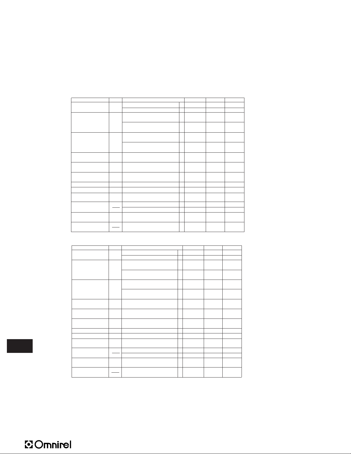
ELECTRICAL CHARACTERISTICS -5 Volt V
= -10V, Io= 500mA, -55°C TA 125°C (unless otherwise specified)
IN
Parameter Symbol Test Conditions Min. Max. Unit
Output Voltage V
Line Regulation V
(Note 1)
Load Regulation V
(Note 1)
Standby Current Drain I
Standby Current Drain DI
Change With Line (Line)
Standby Current Drain DI
Change With Load (Load)
Dropout Voltage V
Peak Output Current I
Short Circuit Current I
(Note 2)
Ripple Rejection DV
Output Noise Voltage N
(Note 3) RMS
Long Term Stability DV
(Note 3) Dt
DV
OUT
RLINE
RLOAD
SCD
SCD
SCD
DO
O (pk)
DS
IN
OUT
O
OUT
ELECTRICAL CHARACTERISTICS -12 Volt V
TA= 25°C -4.9-5.1V
V
= -7.5V to -20V • -4.8-5.2V
IN
VIN= -7.5V to -20V 12 m V
• 25 m V
V
= -8.0V to -12V 5 m V
IN
• 12 m V
IO = 5mA to 1.5 Amp 20 m V
• 25 m V
I
= 250mA to 750 mA 15 m V
O
• 30 m V
2.5 m A
• 3.0 m A
VIN= -7.0V to -20V • 0.4 m A
IO= 5mA to 1000mA • 0.4 m A
DV
= 100mV, I
OUT
= 1.0A • 2.5 V
O
TA= 25°C 1. 5 3. 3 A
VIN= -35V 1. 2 A
• 2.8 A
f =120 Hz, DVIN= -10V 63 d B
(Note 3) • 60 d B
TA= 25°C, f =10 Hz to 100KHz 40 µV/V
TA= 25°C, t = 1000 hrs. 75 m V
= -19V, Io= 500mA, -55°C TA 125°C (unless otherwise specified)
IN
Parameter Symbol Test Conditions Min. Max. Unit
Output Voltage V
Line Regulation V
(Note 1)
Load Regulation V
(Note 1)
Standby Current Drain I
Standby Current Drain DI
Change With Line (Line)
Standby Current Drain DI
Change W ith Load (Load)
Dropout Voltage V
Peak Output Current I
Short Circuit Current I
(Note 2)
Ripple Rejection DV
Output Noise Voltage N
(Note 3) RMS
Long Term Stability DV
(Note 3) Dt
Notes:
1. Load and Line Regulation are specified at a constant junction temperature. Pulse testing with low duty cycle is used.
Changes in output voltage due to heating effects must be taken into account separately.
2. Short Circuit protection is only assured up to V
3. If not tested, shall be guaranteed to the specified limits.
The • denotes the specifications which apply over the full operating temperature range.
DV
OUT
RLINE
RLOAD
SCD
SCD
SCD
DO
O (pk)
DS
IN
OUT
O
OUT
TA= 25°C - 11.76 -12.24 V
= -14.5V to -27V • -1 1.6 -12.4 V
V
IN
VIN= -14.5V to -27V 20 m V
• 50 m V
= -16V to -22V 10 m V
V
IN
• 30 m V
IO = 5mA to 1.5 Amp 32 m V
• 60 m V
= 250mA to 750 mA 16 m V
I
O
• 30 m V
3.5 m A
• 4.0 m A
VIN= -14.5V to -27V • 0.8 m A
IO= 5mA to 1000mA • 0.5 m A
DV
= 100mV, I
OUT
TA= 25°C, IO= 5mA to 1A 1. 5 3 . 3 A
f =120 Hz, DVIN= -10V 56 dB
TA= 25°C, f =10 Hz to 100KHz 40 µV/V
TA= 25°C, t = 1000 hrs. 12 0 m V
IN
= 1.0A • 1.8 V
O
V
= -35V 1. 2 A
IN
• 2.8 A
(Note 3) • 53 dB
= -35V.
3.3 - 2

COM7900T Series
ELECTRICAL CHARACTERISTICS -15 Volt V
= -23V, Io= 500mA, -55°C TA 125°C (unless otherwise specified)
IN
Parameter Symbol Test Conditions Min. Max. Unit
Output Voltage V
Line Regulation V
(Note 1)
OUT
RLINE
TA= 25°C -14.7 -15.3 V
V
= -17.5V to -30V • -14.5 -15.5 V
IN
VIN= -17.5V to -30V 25 m V
• 50 m V
V
= -20V to -26V 15 m V
IN
• 25 m V
Load Regulation V
(Note 1)
RLOAD
IO = 5mA to 1.5 Amp 35 m V
• 75 m V
I
= 250mA to 750 mA 21 m V
O
• 45 m V
Standby Current Drain I
SCD
6.0 m A
• 6.5 m A
Standby Current Drain DI
SCD
Change With Line (Line)
Standby Current Drain DI
SCD
Change With Load (Load)
Dropout Voltage V
Peak Output Current I
Short Circuit Current I
DO
O (pk)
DS
(Note 2)
Ripple Rejection DV
Output Noise Voltage N
IN
DV
OUT
O
(Note 3) RMS
Long Term Stability DV
OUT
(Note 3) Dt
Notes:
1. Load and Line Regulation are specified at a constant junction temperature. Pulse testing with low duty cycle is used.
Changes in output voltage due to heating effects must be taken into account separately.
2. Short Circuit protection is only assured up to V
3. If not tested, shall be guaranteed to the specified limits.
The • denotes the specifications which apply over the full operating temperature range.
VIN= -17.5V to -30V • 0.8 m A
IO= 5mA to 1000mA • 0.5 m A
DV
OUT
= 100mV, I
= 1.0A • 2.5 V
O
TA= 25°C 1. 5 3.3 A
VIN= -35V 1. 2 A
• 2.8 A
f =120 Hz, DVIN= -10V 53 dB
(Note 3) • 50 dB
TA= 25°C, f =10 Hz to 100KHz 40 µV/V
TA= 25°C, t = 1000 hrs. 1 50 m V
= -35V.
IN
TYPICAL PERFORMANCE CHARACTERISTICS
PEAK OUTPUT CURRENT
3.5
3
2.5
2
1.5
1
0.5
DV
= 100mV
OUT
0
05101520253035
Input To Output Differential (V)
Tj= -55°C
Tj= 25°C
Tj= 150°C
DR OPOUT VOLTAGE
2.5
2
1.5
1
0.5
0
-75-50-250255075 100 125 150
I
= 1A
OUT
I
= 500mA
OUT
I
= 0A
OUT
DV
= 100MV
OUT
Junction Temperature (°C)
3.3 - 3
RIPPLE REJECTION
100
80
60
40
V
IN
20
0
10 100 1k10k 100k
Frequency (Hz)
- V = 8V
I
T
OUT
j
= 1A
= 25°C
V
= 5V
OUT
+3.5V
DC
rms
3.3

205 Crawford Street, Leominster, MA 01453 USA (978) 534-5776 FAX (978) 537-4246
COM7900T Series
.430
.410
.200
.190
.038 MAX.
.005
.120 TYP.
.537
.527
.665
.645
.420
.410
.150
.140
.750
.500
.100 TYP.
.035
.025
.045
.035
V
IN
V
OUT
1µF2.2µF
1
32
COM79XX
++
V
IN
I
OU
3
1
2
2.2µF
R1
OM79XX
I
Q
I
OUT
=
V
OUT
R1
+ I
Q
Input bypass capacitors are recommended for stable operation of the OM7900 series of regulators over
the input voltage and output current ranges. Output bypass capacitors will improve the transient
response of the regulator.
The bypass capacitors, (2.2µF on the input, 1µF on the output) should be ceramic or solid tantalum which
have good high frequency characteristics. If aluminum electrolytics are used, their values should be 10µF
or larger. The bypass capacitors should be mounted with the shortest leads, and if possible, directly
across the regulator terminals.
Fixed Output Regulator Basic Current Regulator
TYPICAL APPLICATIONS
MECHANICAL OUTLINE PIN CONNECTION
TO-257AA
3.3
Note:
• Case is metal/hermetically sealed
• Isolated Tab/Glass Feedthroughs
COM79XXT
Isolated
Front View
Pin 1: Ground
Pin 2: Input
Pin 3: Output
Tab: Isolated
Tab
123
 Loading...