

Page 1

www.omega.com
e-mail: info@omega.com
User’s Guide
OME-TMC12(A)
PCI-Bus Digital I/O
Board
Hardware Manual
Shop online at
Page 2

Servicing North America:
USA: One Omega Drive, P.O. Box 4047
ISO 9001 Certified Stamford CT 06907-0047
TEL: (203) 359-1660 FAX: (203) 359-7700
e-mail: info@omega.com
Canada: 976 Bergar
Laval (Quebec) H7L 5A1, Canada
TEL: (514) 856-6928 FAX: (514) 856-6886
e-mail: info@omega.ca
For immediate technical or application assistance:
USA and Canada: Sales Service: 1-800-826-6342 / 1-800-TC-OMEGA
®
Customer Service: 1-800-622-2378 / 1-800-622-BEST
®
Engineering Service: 1-800-872-9436 / 1-800-USA-WHEN
®
TELEX: 996404 EASYLINK: 62968934 CABLE: OMEGA
Mexico: En Espan˜ ol: (001) 203-359-7803 e-mail: espanol@omega.com
FAX: (001) 203-359-7807 info@omega.com.mx
Servicing Europe:
Benelux: Postbus 8034, 1180 LA Amstelveen, The Netherlands
TEL: +31 (0)20 3472121 FAX: +31 (0)20 6434643
Toll Free in Benelux: 0800 0993344
e-mail: sales@omegaeng.nl
Czech Republic: Frystatska 184, 733 01 Karviná, Czech Republic
TEL: +420 (0)59 6311899 FAX: +420 (0)59 6311114
Toll Free: 0800-1-66342 e-mail: info@omegashop.cz
France: 11, rue Jacques Cartier, 78280 Guyancourt, France
TEL: +33 (0)1 61 37 29 00 FAX: +33 (0)1 30 57 54 27
Toll Free in France: 0800 466 342
e-mail: sales@omega.fr
Germany/Austria: Daimlerstrasse 26, D-75392 Deckenpfronn, Germany
TEL: +49 (0)7056 9398-0 FAX: +49 (0)7056 9398-29
Toll Free in Germany: 0800 639 7678
e-mail: info@omega.de
United Kingdom: One Omega Drive, River Bend Technology Centre
ISO 9002 Certified Northbank, Irlam, Manchester
M44 5BD United Kingdom
TEL: +44 (0)161 777 6611 FAX: +44 (0)161 777 6622
Toll Free in United Kingdom: 0800-488-488
e-mail: sales@omega.co.uk
OMEGAnet®Online Service Internet e-mail
www.omega.com info@omega.com
It is the policy of OMEGA to comply with all worldwide safety and EMC/EMI regulations that
apply. OMEGA is constantly pursuing certification of its products to the European New Approach
Directives. OMEGA will add the CE mark to every appropriate device upon certification.
The information contained in this document is believed to be correct, but OMEGA Engineering, Inc. accepts
no liability for any errors it contains, and reserves the right to alter specifications without notice.
WARNING: These products are not designed for use in, and should not be used for, patient-connected applications.
Page 3

OME-PCI-TMC12(A)
User Manual
OME-PCI-TMC12(A) User Manual (Ver. 2.0, Sep/2002) --- 1
Page 4

Tables of Contents
1.
1. INTRODUCTION ....................................................................................................................4
1.1 OME-PCI-TMC12(A)........................................................................................................5
1.2 PRODUCT CHECK LIST ........................................................................................................5
2. HARDWARE CONFIGURATION ........................................................................................6
2.1 BOARD LAYOUT.................................................................................................................. 6
2.2 COUNTER ARCHITECTURE...................................................................................................7
2.3 D/I/O BLOCK DIAGRAM...................................................................................................... 8
2.4 JUMPER SETTING................................................................................................................. 9
2.5 DAUGHTER BOARDS ......................................................................................................... 13
2.6 PIN ASSIGNMENT ..............................................................................................................17
3. I/O CONTROL REGISTER......................................................................................................19
3.1 HOW TO FIND THE I/O ADDRESS........................................................................................19
3.2 THE ASSIGNMENT OF I/O ADDRESS ...................................................................................21
3.3 THE I/O ADDRESS MAP ..................................................................................................... 22
3.4 NEW FEATURES OF OME-PCI-TMC12A..........................................................................27
4. 8254 PROGRAMMING ........................................................................................................ 32
4.1 CONTROL WORD FORMAT ................................................................................................ 32
4.2 COUNTER LATCH COMMAND .............................................................................................33
4.3 READ BACK COMMAND .....................................................................................................33
4.4 STATUS BYTE FORMAT ......................................................................................................33
5. DEMO PROGRAM....................................................................................................................34
5.1 DEMO1: USE D/O................................................................................................................. 35
5.2 DEMO2: USE D/I ..................................................................................................................36
5.3 DEMO3: WAVE GENERATOR ................................................................................................37
5.4 DEMO4: DELAY ONE MSEC...................................................................................................39
5.5 DEMO5: 16-BIT EVENT COUNTER.........................................................................................40
5.6 DEMO6: SOFTWARE COUNTER .............................................................................................41
5.7 DEMO7: WATCHDOG TIMER.................................................................................................42
5.8 DEMO8: PULSE WIDTH MEASURE ........................................................................................44
5.9 DEMO9: FREQUENCY MEASURE...........................................................................................46
5.10 DEMO10: FIND CARD NUMBER ............................................................................................48
5.11 DEMO11: COUNT LOW PULSE ..............................................................................................49
5.12 DEMO12: LOW PULSE WIDTH ..............................................................................................51
OME-PCI-TMC12(A) User Manual (Ver. 2.0, Sep/2002) --- 2
Page 5

5.13 DEMO13: HIGH PULSE WIDTH ............................................................................................. 54
5.14 NDEMO1: USING LEDS ........................................................................................................56
5.15 NDEMO2: GENERATE 2 CLOCKS...........................................................................................57
5.16 NDEMO3: NEW DEMO7 ........................................................................................................60
5.17 NDEMO4: ACTIVE HIGH INT .................................................................................................63
5.18 NDEMO5: ACTIVE LOW INT.................................................................................................. 66
OME-PCI-TMC12(A) User Manual (Ver. 2.0, Sep/2002) --- 3
Page 6

1. Introduction
• The OME-PCI-TMC12(A) is a general purpose counter/timer and digital I/O card
• PC AT compatible PCI bus
• On-board four 8254 chips
• 5 different interrupt sources, 4 internal + 1 external, jumper selectable
• Flexible clock sources and gate control signals selectable
• 2 stable internal clock sources, CLOCK1=8M/1.6M, CLOCK2=0.8M/80K,
jumper selectable
• 12 external clock sources
• 12 external gate control signals
• 16 bits general purpose TTL-compatible D/O or relay (with daughter board OME-
DB-16R or OME-DB-24PR)
• 16 bits general propose TTL-compatible D/I or isolated input (with daughter
board OME-DB-16P)
• 12 independent 16 bits timer/counter
• All signals are TTL compatible
• Operating Temperature: 0°C to 60°C
• Storage Temperature: -20°C to 80°C
• Humidity: 0 to 90% RH non-condensing
• Dimension: 150mm X 105mm
• Power Consumption: +5V @ 500mA
Note: PCI_TMC12(A) = OME-PCI-TMC12 or OME-PCI-TMC12A
OME-PCI-TMC12(A) User Manual (Ver. 2.0, Sep/2002) --- 4
Page 7

1.1 OME-PCI-TMC12(A)
• All old programs designed for OME-PCI-TMC12 can be executed on OME-PCI-
TMC12A without any modification
• OME-PCI-TMC12A provides additional features to OME-PCI-TMC12, refer to
Sec. 3.4 for more information.
1.2 Product Check List
In addition to this manual, the package includes the following items:
• OME-PCI-TMC12(A) card
• One companion CD for software driver & related documents
Attention!
If any of these items are missing or damaged, contact Omega Engineering
immediately. Save the shipping materials and the box in case you want to ship or
store the product.
OME-PCI-TMC12(A) User Manual (Ver. 2.0, Sep/2002) --- 5
Page 8

2. Hardware configuration
K
2.1 Board Layout
PCI BUS
J22, J23, J24
J19, J20, J21
J16, J17, J18
EXT
SPARE
J13, J14, J15
CH9
CH12
80
1.6M
J10, J11, J12
CH3
CH6
800K
CLOCK2
8M
CLOCK1
J7, J8, J9
J25
J26
J27
J4, J5, J6
J1, J2, J3
LED2 LED1
LED3
OMEPCI-TMC12 /OME- PCI-TMC12A
Note: J28, LED1, LED2 & LED3 are designed for OME-PCI-TMC12A only.
OME-PCI-TMC12(A) User Manual (Ver. 2.0, Sep/2002) --- 6
PCI BUS
D/I
TMC12A
CON2
TMC-12
Int
J28
CON3
D/O
Page 9

2.2 Counter Architecture
G
G
G
G
G
G
G
G
G
G
G
G
There are four 8254 chips on the OME-PCI-TMC12(A) card. The block diagram is
given as following:
CLK1
GATE1
CLK2
GATE2
8254 CHIP #1 (U12)
Counter 1
CLK
OUT
ATE
Counter 2
CLK
OUT
ATE
CLK4
COUT1
GATE4
CLK5
COUT2
GATE5
8254 CHIP #2 (U8)
Counter 4
CLK
OUT
ATE
Counter 5
CLK
OUT
ATE
COUT4
COUT5
CLK3
GATE3
CLK7
GATE7
CLK8
GATE8
CLK9
GATE9
Counter 3
CLK
OUT
ATE
8254 CHIP #3 (U3)
Counter 7
CLK
OUT
ATE
Counter 8
CLK
OUT
ATE
Counter 9
CLK
OUT
ATE
COUT3
COUT7
COUT8
COUT9
CLK6
GATE6
CLK10
GATE10
CLK11
GATE11
CLK12
GATE12
Counter 6
CLK
OUT
ATE
8254 CHIP #4 (U1)
Counter 10
CLK
OUT
ATE
Counter 11
CLK
OUT
ATE
Counter 12
CLK
OUT
ATE
COUT6
COUT10
COUT11
COUT12
OME-PCI-TMC12(A) User Manual (Ver. 2.0, Sep/2002) --- 7
Page 10

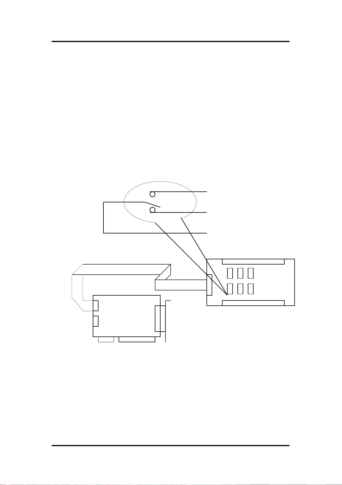
2.3 D/I/O Block Diagram
The OME-PCI-TMC12(A) provides 16 digital input channels and 16 digital
output channels. All levels are TTL compatible. The connections diagram and block
diagram are given as following:
I/O read
signal
Local Data Bus
DO port
D0..D15
I/O write
signal
DI port
CON3
CON2
The D/I port can be connected to the OME-DB-16P. The OME-DB-16P is a 16-
channel isolated digital input daughter board. The D/O port can be connected to the
OME-DB-16R or OME-DB-24PR. The OME-DB-16R is a 16-channel relay output
board. The OME-DB-24R is a 24-channel power relay output board.
OME-PCI-TMC12(A) User Manual (Ver. 2.0, Sep/2002) --- 8
Page 11

2.4 Jumper Setting
K
2.4.1 CLOCK1 & CLOCK2
There are two stable internal clock sources in OME-PCI-TMC12(A) which named
as CLOCK1 & CLOCK2. The CLOCK1 may be 8M or 1.6M selectable by J27. The
CLOCK2 may be 0.8M or 80K selected by J26. The block diagram of internal clock
sources is given as following:
8 M
CLOCK1= 8M
1.6 M 0.8M
J27 select
CLOCK1
8M
CLOCK1
1.6M
CLOCK1= 1.6M
800K
CLOCK2
80
80 K
J26
select
CLOCK2
8M
CLOCK1
1.6M
800K
CLOCK2
80K
OME-PCI-TMC12(A) User Manual (Ver. 2.0, Sep/2002) --- 9
CLOCK2= 800K
CLOCK2= 80K
Page 12

2.4.2 CLK1 to CLK12
1: select CLOCK1
2: select CLOCK2
5: select COUTn-1
6: select external CLKn from CN1
Select
CLOCK1
Select
COUTn-1
(last channel)
1 2
5 6
1 2
5 6
Select
CLOCK2
Select
EXT_CLKn
(external
CLKn)
1 2
5 6
1 2
5 6
CLK1-12 jumper Select sources
CLK1 JP22 CLOCK1, CLOCK2, COUT6, ECLK1
CLK2 JP23 CLOCK1, CLOCK2, COUT1, ECLK2
CLK3 JP24 CLOCK1, CLOCK2, COUT2, ECLK3
CLK4 JP13 CLOCK1, CLOCK2, COUT3, ECLK4
CLK5 JP14 CLOCK1, CLOCK2, COUT4, ECLK5
CLK6 JP15 CLOCK1, CLOCK2, COUT5, ECLK6
CLK7 JP10 CLOCK1, CLOCK2, COUT12, ECLK7
CLK8 JP11 CLOCK1, CLOCK2, COUT7, ECLK8
CLK9 JP12 CLOCK1, CLOCK2, COUT8, ECLK9
CLK10 JP1 CLOCK1, CLOCK2, COUT9, ECLK10
CLK11 JP2 CLOCK1, CLOCK2, COUT10, ECLK11
CLK12 JP3 CLOCK1, CLOCK2, COUT11, ECLK12
OME-PCI-TMC12(A) User Manual (Ver. 2.0, Sep/2002) --- 10
Page 13

2.4.3 GATE1 TO GATE12
GATE Jumper Select source
GATE1 J19 Inverted COUT6, EXTG1
GATE2 J20 Inverted COUT1, EXTG2
GATE3 J21 Inverted COUT2, EXTG3
GATE4 J16 Inverted COUT3, EXTG4
GATE5 J17 Inverted COUT4, EXTG5
GETE6 J18 Inverted COUT5, EXTG6
GATEn = EXTGn
3
2
1
GATEn = Inverted COUTn-1
3
2
1
GATE Jumper Select source
GATE7 J7 COUT12, EXTG7
GATE8 J8 COUT7, EXTG8
GATE9 J9 COUT8, EXTG9
GATE10 J4 COUT9, EXTG10
GATE11 J5 COUT10, EXTG11
GETE12 J6 COUT11, EXTG12
GATEn = EXTGn
3
2
1
3
2
1
GATEn = COUTn-1
OME-PCI-TMC12(A) User Manual (Ver. 2.0, Sep/2002) --- 11
Page 14

2.4.4 J25: Interrupt Source Selection
(
(
)
(
(
)
There are five signals can be used as interrupt sources: CH3, CH6, CH9, CH12 &
EXT as following:
CH3: comes from COUT3, output of counter 3
CH6: comes from COUT6, output of counter 6
CH9: comes from COUT9, output of counter 9
CH12: comes from COUT12, output of counter 12
EXT: comes from ECLK11, external CLK for counter 11, from CN1.
(SPARE): no interrupt source
SPARE)
Interrupt source=ECLK11
SPARE)
No interrupt source
CH3
CH6
CH9
CH12
EXT
CH3
CH6
CH9
CH12
EXT
CH3
CH6
CH9
CH12
EXT
SPARE
Interrupt source=COUT6
CH3
CH6
CH9
CH12
EXT
SPARE
Interrupt source=COUT3
OME-PCI-TMC12(A) User Manual (Ver. 2.0, Sep/2002) --- 12
Page 15

2.5 Daughter Boards
2.5.1 OME-DB37
The OME-DB-37 is a general purpose daughter board for D-sub 37 pins. It is
designed for easy wire connection.
2.5.2 OME-DN37 & OME-DN20
The OME-DN-37 is a general purpose daughter board for D-sub 37 pins. The
OME-DN-20 is designed for the 20-pin flat-cable. They are designed for easy wire
connection. These boards are DIN-Rail mountable.
37pin cable
OME-DN-37
2.5.3 OME-DB-8125 & OME-DB-8025
The OME-DB-8125 is a general purpose screw terminal board. It is designed for
ease of wiring. There is one D-sub 37-pin connector & two 20-pin flat-cable headers in
the OME-DB-8125. The OME-DB-8025 is designed for 20-pin flat-cable header.
OME-PCI-TMC12(A) User Manual (Ver. 2.0, Sep/2002) --- 13
37pin cable
OME-DB-8125
(D-sub 37 or
20-pin flat-cable header)
Page 16

2.5.4 OME-DB-16P Isolated Input Board
The OME-DB-16P is a 16-channel isolated digital input daughter board. The
optically isolated inputs of the OME-DB-16P consist of a bi-directional opto-coupler
with a resistor for current sensing. You can use the OME-DB-16P to sense DC signal
from TTL levels up to 24V or use the OME-DB-16P to sense a wide range of AC
signals. You can use this board to isolate the computer from large common-mode
voltage, ground loops and transient voltage spike that often occur in industrial
environments.
OME-PCI-TMC12 D/I
Opto-Isolated
OME-PCI-TMC12(A)
CON2=D/I
20-Pin cable
OME-DB-16P
AC or DC Signal
0V to 24V
+
-
OME-PCI-TMC12(A) User Manual (Ver. 2.0, Sep/2002) --- 14
Page 17
2.5.5 OME-DB-16R Relay Board
The OME-DB-16R, 16-channel relay output board, consists of 16 form C relays
for efficient switching of load by programmed control. The relays are energized by
applying 5 volt signal to the appropriated relay channel on the 20-pin flat connector.
There are 16 enunciator LEDs for each relay. They light when their associated relays
are activated. To avoid overloading your PC’s power supply, this board provides a
screw terminal for external power supply.
From C Relay
20Pin cable
CON3=D/O
OME-PCI-TMC12(A)
Normal Open
Normal Close
Com
OME-DB-16R
Note:
Channel: 16 From C Relay
Relay: Switching up to 0.5A at 110ACV
or 1A at 24DCV
OME-PCI-TMC12(A) User Manual (Ver. 2.0, Sep/2002) --- 15
Page 18

2.5.6 OME-DB-24PR/24POR/24C
OME-DB-24PR 24*power relay, 5A/250V
OME-DB-24POR 24*photo MOS relay, 0.1A/350VAC
OME-DB-24C 24*open collector, 100mA per channel, 30V max.
The OME-DB-24PR, 24-channel power relay output board, consists of 8 form C
and 16 form A electromechanical relays for efficient switching of load by
programmed control. The contact of each relay can control a 5A load at
250ACV/30VDCV. The relay is energized by applying a 5 volt signal to the
appropriate relay channel on the 20-pin flat cable connector (only uses 16 relays) or
50-pin flat cable connector.(compatible to the OME-DIO-24 series). Twenty four
enunciator LEDs (one for each relay) light when their associated relay is activated. To
avoid overloading your PC’s power supply, this board needs a +12VDC or +24VDC
external power supply.
Normal Open
From A Relay
Com
20Pin cable
To 20pin connector
OME-DB-24PR
CON3=D/O
OME-PCI-TMC12(A)
Note:
50-Pin connector (compatible with OME-DIO-24/48/144)
20-Pin connector for 16-channel digital outputs (Compatible with OME-A-82X, OME-
A-62X, OME-DIO-64, OME-ISO-DA16/DA8)
Channel: 16 Form A Relays, 8 Form C Relays
Relay: switching up to 5A at 110ACV / 5A at 30DCV
OME-PCI-TMC12(A) User Manual (Ver. 2.0, Sep/2002) --- 16
Page 19

2.6 Pin Assignment
The CON1 is a 37-pin D-type female connector.
Pin Number Description Pin Number Description
1 ECLK1 20 EXTG1
2 COUT1 21 ECLK2
3 EXTG2 22 COUT2
4 ECLK3 23 EXTG3
5 COUT3 24 ECLK4
6 EXTG4 25 COUT4
7 ECLK5 26 EXTG5
8 COUT5 27 ECLK6
9 EXTG6 28 COUT6
10 ECLK7 29 EXTG7
11 COUT7 30 ECLK8
12 EXTG8 31 COUT8
13 ECLK9 32 EXTG9
14 COUT9 33 ECLK10
15 EXTG10 34 COUT10
16 ECLK11 35 EXTG11
17 COUT11 36 ECLK12
18 EXTG12 37 COUT12
19 GND XXXXXXX This pin not available
ECLKn: external clock source for counter n
EXTGn: external gate control signal for counter n
COUTn: output of timer/counter n
All signals are TTL compatible.
OME-PCI-TMC12(A) User Manual (Ver. 2.0, Sep/2002) --- 17
Page 20

CON2: pin assignment of digital input connector.
Pin Name Pin Name
1 Digital input 0 2 Digital input 1
3 Digital input 2 4 Digital input 3
5 Digital input 4 6 Digital input 5
17 Digital input 6 8 Digital input 7
9 Digital input 8 10 Digital input 9
11 Digital input 10 12 Digital input 11
13 Digital input 12 14 Digital input 13
15 Digital input 14 16 Digital input 15
17 PCB ground 18 PCB ground
19 PCB +5V 20 PCB +12V
CON3: pin assignment of the digital output connector.
Pin Name Pin Name
1 Digital output 0 2 Digital output 1
3 Digital output 2 4 Digital output 3
5 Digital output 4 6 Digital output 5
17 Digital output 6 8 Digital output 7
9 Digital output 8 10 Digital output 9
11 Digital output 10 12 Digital output 11
13 Digital output 12 14 Digital output 13
15 Digital output 14 16 Digital output 15
17 PCB ground 18 PCB ground
19 PCB +5V 20 PCB +12V
OME-PCI-TMC12(A) User Manual (Ver. 2.0, Sep/2002) --- 18
Page 21

3. I/O Control Register
3.1 How to Find the I/O Address
The plug & play BIOS will assign a proper I/O address to every OME-PCI-
TMC12(A) card in the power-on stage. The IDs of OME-PCI-TMC12(A) are given
as following:
• Vendor ID = 10B5
• Device ID = 9050
• Sub-vendor ID= 2129
• Sub-device ID = 9912
We provide all necessary functions as following:
1. PTMC12_DriverInit(&wBoard)
This function can detect how many OME-PCI-TMC12(A) cards in the system.
It is implemented based on the PCI plug & play mechanism. It will find all
OME-PCI-TMC12(A) cards installed in this system & save all their resource
in the library.
• wBoard=1 Æ only one OME-PCI-TMC12(A) in this PC system.
• wBoard=2 Æ there are two OME-PCI-TMC12(A) in this PC system.
2. PTMC12_GetConfigAddressSpace(wBoardNo,*wBase,*wIrq,*wPLX)
The user can use this function to save resource of all OME-PCI-TMC12(A)
installed in this system. Then the application program can control all
functions of OME-PCI-TMC12(A) directly.
• wBoardNo=0 to N Æ totally N+1 cards of OME-PCI-TMC12(A)
• wBase Æ base address of the board control word
• wIrq Æ allocated IRQ channel number of this board
• wPLX Æ base address of PCI-interface-IC
OME-PCI-TMC12(A) User Manual (Ver. 2.0, Sep/2002) --- 19
Page 22

The sample program source is given as following:
/* step1: detect all OME-PCI-TMC12(A) card first */
wRetVal=PTMC12_DriverInit(&wBoards);
printf("Threr are %d OME-PCI-TMC12 Cards in this PC\n",wBoards);
/* step2: save resource of all OME-PCI-TMC12(A) cards installed in this PC */
for (i=0; i<wBoards; i++)
{
PTMC12_GetConfigAddressSpace(i,&wBase,&wIrq,&wPLX);
printf("\nCard_%d: wBase=%x, wIrq=%x, wPLX=%x", i,wBase,wIrq,wPLX);
wConfigSpace[i][0]=wBaseAddress; /* save all resource of this card */
wConfigSpace[i][1]=wIrq; /* save all resource of this card */
wConfigSpace[i][2]=wPLX; /* save all resource of this card */
}
/* step3: control the OME-PCI-TMC12(A) directly */
wBase=wConfigSpace[0][0]; /* get base address the card_0 */
outport(wBase+0x14,wDoValue); /* control the D/O states of card_0 */
wDiValue=inport(wBase+0x14); /* read the D/I states of card_0 */
wBase=wConfigSpace[1][0]; /* get base address of card_1 */
outport(wBase+0x14,wDoValue); /* control the D/O states of card_1 */
wDiValue=inport(wBase+0x14); /* read the D/I states of card_1 */
wPLX=wConfigSpace[2][2]; /* get PCI-interface base address of card-
2 */
_outpd(wPLX+0x4c,0x41); /* channel_1, interrupt active_Low */
..
..
_outpd(wPLX+0x4c,0); /* disable all interrupt */
OME-PCI-TMC12(A) User Manual (Ver. 2.0, Sep/2002) --- 20
Page 23

3.2 The Assignment of I/O Address
The plug & play BIOS will assign the proper I/O address to OME-PCI-TMC12.
If there is only one OME-PCI-TMC12, the user can identify the board as card_0. If
there are two OME-PCI-TMC12 cards in the system, the user will be very difficult
to identify which board is card_0? The software driver can support 16 boards max.
Therefore the user can install 16 boards of OME-PCI-TMC12 in one PC system.
How to find the card_0 & card_1 ?
The simplest way to find the card number is to use DEM10.EXE given in
DOS demo program. This demo program will send a value to D/O and read back
from D/I. If the user installs a 20-pin flat cable between CON2 & CON3, the value
read from D/I will be the same as D/O. The operation steps are given as following:
1. Remove all 20-pin flat cable between CON2 and CON3
2. Install all OME-PCI-TMC12 cards into this PC system
3. Power-on and run DEM10.EXE
4. Now all D/I values will be different from the D/O values
5. Install a 20-pin flat cable into CON2 & CON3 of any OME-PCI-TMC12
card
6. There will be one card’s D/I value = D/O value, the card number is also
show in screen
Therefore the user can find the card number if he install a 20-pin flat cable into
OME-PCI-TMC12 sequentially.
OME-PCI-TMC12(A) User Manual (Ver. 2.0, Sep/2002) --- 21
Page 24

3.3 The I/O Address Map
The I/O address of OME-PCI-TMC12(A) is automatically assigned by
the main board ROM BIOS. The I/O address can also be re-assigned by user.
It is strongly recommended to the user to not change the I/O address.
The plug & play BIOS will assign proper I/O address to each OME-PCI-
TMC12(A). The hardware I/O ports are described as following:
Address Read Write
wBase+0 Active 8254 Counter 0 Active 8254 Counter 0
wBase+4 Active 8254 Counter 1 Active 8254 Counter 1
wBase+8 Active 8254 Counter 2 Active 8254 Counter 2
wBase+0x0C Active 8254 Control word Active 8254 Control word
wBase+0x10 Reserved Select the active 8254 chip
wBase+0x14 Digital input channel 0-15 Digital output channel 0-15
wBase+0x18 New control of OME-PCI-
TMC12A
Note. Refer to Sec. 3.1 for more information about wBase.
Interrupt clear of OME-PCI-
TMC12A
3.3.1 Select the active 8254 chip 1/2/3/4
There are four 8254 chips in OME-PCI-TMC12(A) card. Only one 8254 is active at
the same time. Before using the active 8254, use wBase+0x10 to select the active
8254.
(WRITE) wBase+0x10: select the active 8254 chip
Bit 7 Bit 6 Bit 5 Bit 4 Bit 3 Bit 2 Bit 1 Bit 0
X X X X X X D1 D0
Note. Refer to Sec. 3.1 for more information about wBase.
D0=0, D1=0: 8254 chip-1 is active
D0=1, D1=0: 8254 chip-2 is active
D0=0, D1=1: 8254 chip-3 is active
D0=1, D1=1: 8254 chip-4 is active
outportb(wBase+0x10,0); /* select the 8254 chip-1, CNT1 ~CNT3 */
outportb(wBase+0x10,2); /* select the 8254 chip-3 , CNT10 ~ CNT12 */
OME-PCI-TMC12(A) User Manual (Ver. 2.0, Sep/2002) --- 22
Page 25

3.3.2 8254 Timer/Counter Control
There are four 8254 chips in OME-PCI-TMC12(A) card. Only one 8254 is
active at any instant. Before using the active 8254, use wBase+0x10 to select the
active. The 8254 has 4 registers from wBase+0 through wBase+0x0C. For detailed
programming information about 8254, please refer to Chapter 4 & Intel’s
“Microsystem Components Handbook”.
Address Read Write
wBase+0 Active 8254 Counter 0 Active 8254 Counter 0
wBase+4 Active 8254 Counter 1 Active 8254 Counter 1
wBase+8 Active 8254 Counter 2 Active 8254 Counter 2
wBase+0x0C Active 8254 Control word Active 8254 Control word
Note. Refer to Sec. 3.1 for more information about wBase.
3.3.3 Digital Input
(READ) wBase+0x14: read the digital input channel 0 to 15
Bit 7 Bit 6 Bit 5 Bit 4 Bit 3 Bit 2 Bit 1 Bit 0
DI7 DI6 DI5 DI4 DI3 DI2 DI1 DI0
Bit 15 Bit 14 Bit 13 Bit 12 Bit 11 Bit 10 Bit 9 Bit 8
DI15 DI14 DI13 DI12 DI11 DI10 DI9 DI8
Note. Refer to Sec. 3.1 for more information about wBase.
wDiValue=inport(wBase+0x14); /* read the D/I states */
OME-PCI-TMC12(A) User Manual (Ver. 2.0, Sep/2002) --- 23
Page 26

3.3.4 Digital Output
(WRITE) wBase+0x14: set the digital output channel 0 to 15
Bit 7 Bit 6 Bit 5 Bit 4 Bit 3 Bit 2 Bit 1 Bit 0
DO7 DO6 DO5 DO4 DO3 DO2 DO1 DO0
Bit 15 Bit 14 Bit 13 Bit 12 Bit 11 Bit 10 Bit 9 Bit 8
DO15 DO14 DO13 DO12 DO11 DO10 DO9 DO8
Note. Refer to Sec. 3.1 for more information about wBase.
outport(wBase+0x14,wDoValue); /* control the D/O states */
3.3.5 Interrupt control/status register of OME-
PCI-TMC12
(READ/WRITE) wPLX+0x4C: interrupt control/status register
Bit Description
B0 INTERRUPT enable, 0=disable, 1=enable
B1 POLARITY, 1=active HIGH, 0=active LOW
B2 INTERRUPT status, 0=int not active, 1=int is active
B3 reserved
B4 reserved
B5 reserved
B6 PCI interrupt enable, 0=disable, 1=enable
B7 Software interrupt, a value of 1 will generate interrupt
B8 to
B31
Refer to DEMO7.C, DEMO11.C, DEMO12.C & DEMO13.C for more information.
reserved
The interrupt of OME-PCI-TMC12 is level-trigger. The interrupt signal can be
programmed active-low or active-high. The procedures of programming are
given as following:
OME-PCI-TMC12(A) User Manual (Ver. 2.0, Sep/2002) --- 24
Page 27

1. make sure the initial level is High or Low
2. if the initial state is High Æ set the interrupt signal is active_low initially
3. if the initial state is Low Æ set the interrupt signal is active_high initially
4. If the interrupt signal is active Æ program will transfer into the interrupt
service routine Æ toggle the active_state before return from the ISR.
Example 1: assume initial level=High
Initial=High
Initial_sub()
{ now_int_state=1
_outpd(wPLX+0x4c,0x41)
(INT signal is active_Low)
ISR_sub()
{
If (now_int_state==0) /* old state=low Æ change to high now */
{
now_int_state=1; /* now int_signal is High */
*** application codes are given here ***
_outpd(wPLX+0x4c,0x41);/* active Low */
}
else /* old state=highÆ change to low now */
{
now_int_state=0; /* now int_signal is Low */
*** application codes are given here ***
_outpd(wPLX+0x4c,0x43);/* active High */
}
if (wIrq>=8) outportb(A2_8259,0x20); /* EOI */
outportb(A1_8259,0x20); /* EOI */
}
OME-PCI-TMC12(A) User Manual (Ver. 2.0, Sep/2002) --- 25
Page 28

Example 2: assume initial level=Low
Initial=Low
Initial_sub()
{ now_int_state=0
_outpd(wPLX+0x4c,0x43)
(INT signal is
ISR_sub()
{
If (now_int_state==0) /* old state=low Æ change to high now */
{
now_int_state=1; /* now int_signal is High */
*** application codes are given here ***
_outpd(wPLX+0x4c,0x41);/* active Low */
}
else /* old state=highÆ change to low now */
{
now_int_state=0; /* now int_signal is Low */
*** application codes are given here ***
_outpd(wPLX+0x4c,0x43);/* active High */
}
if (wIrq>=8) outportb(A2_8259,0x20); /* EOI */
outportb(A1_8259,0x20); /* EOI */
}
So the ISR_sub( ) will be active on the rising edge & falling edge of the
interrupt signal. Refer to demo7.c, demo11.c, demo12.c & demo13.c for more
information.
OME-PCI-TMC12(A) User Manual (Ver. 2.0, Sep/2002) --- 26
Page 29

3.4 New features of OME-PCI-
TMC12A
3.4.1 Default Settings of OME-PCI-TMC12A
The default settings of J28 (when board is shipped) on OME-PCI-
TMC12A(Sec. 3.4.4) makes it is equivalent to OME-PCI-TMC12. So the interrupt
system of OME-PCI-TMC12A in the default setting is compatible to OME-PCI-
TMC12. Refer to Sec. 3.4.4 for interrupt block diagram of OME-PCI-TMC12 &
OME-PCI-TMC12A.
All Xor? of OME-PCI-TMC12A are clear to their Low states in the first
power-up stage, so all clock sources of OME-PCI-TMC12A are compatible to
those of OME-PCI-TMC12. Refer to Sec. 3.4.2 for block diagram.
As shipped the OME-PCI-TMC12A is used as an OME-PCI-TMC12. All old
application programs designed for OME-PCI-TMC12 can be executed in
OME-PCI-TMC12A without any modification.
Key point Æ Default factory settings of OME-PCI-TMC12A
makes it equivalent to an OME-PCI-TMC12
The new features of OME-PCI-TMC12A are given as follows:
z The new interrupt mechanism (Sec. 3.4.4)
z The Xor? bits for 2 clocks generation (Sec. 3.4.2)
z There are 3 LEDs for status indicators (Sec. 3.4.3 & Sec. 2.1)
z It equips one smith trigger buffer for the selected clock source (Sec. 3.4.2)
z One new D/O port, wBase+0x18, for Xor-bits, XorInt & LED on/off control.
Refer to Sec. 3.4.3 for more information.
z One new D/I port, wBase+0x18, for interrupt enable. The initial routine &
ISR must inport from wBase+0x18 to enable next interrupt operation. Refer to
Sec. 3.4.4 for more information.
z Refer to new demo programs given in Sec. 3.4.5 for using these new features.
z Refer to Sec. 2.1 for PCB layout of OME-PCI-TMC12A
OME-PCI-TMC12(A) User Manual (Ver. 2.0, Sep/2002) --- 27
Page 30

3.4.2 Clock input of 8254
The clock input of 8254 chips in OME-PCI-TMC12 is given as follows:
Select
Clock source
(Sec. 2.4.3)
(default select clock1)
The clock input of 8254 chips in OME-PCI-TMC12A is given as follows:
Xor-control Register
(Sec. 3.4.3)
Select
Clock source
(Sec. 2.4.3)
1 2
5 6
1 2
5 6
Schmidt
Trigger
Buffer
Clock input
of 8254
Xor logic
Clock input
of 8254
(default select clock1)
The new features of OME-PCI-TMC12A are given as follows:
z A schmidt trigger buffer is added to remove noises in the selected clock
source
z A Xor-control register is added to invert/non-inverted the selected clock
source. This mechanism can be used to generate 2 extra starting clocks to
8254.
Note: The Xor-control register is clear to 0 when the OME-PCI-TMC12A is
first power-up. So the initial state of OME-PCI-TMC12A is exactly compatible to
OME-PCI-TMC12.
Refer to Sec. 5.15 Ndemo2: Generate 2 Clocks, the twelve Xor-bits are used to
generate the 2 starting clocks. So the initial value of 8254 can be verified after these 2
starting clocks are generated. Then they are used to generate one single clock for
testing. In general, these Xor-bits are designed for generation of 2 starting clocks only.
OME-PCI-TMC12(A) User Manual (Ver. 2.0, Sep/2002) --- 28
Page 31

3.4.3 Xor-control Register of OME-PCI-
TMC12A
(WRITE) wBase+0x18: set the Xor-control register
Bit 7 Bit 6 Bit 5 Bit 4 Bit 3 Bit 2 Bit 1 Bit 0
Xor8 Xor7 Xor6 Xor5 Xor4 Xor3 Xor2 Xor1
Bit 15 Bit 14 Bit 13 Bit 12 Bit 11 Bit 10 Bit 9 Bit 8
Led3 Led2 Led1 XorInt Xor12 Xor11 Xor10 Xor9
Note 1. Refer to Sec. 3.1 for more information about wBase.
Note 2. All bits of this register will be clear to zero in the power-up stage.
Xor1 --> invert/non-invert the selected clock source of CLK1
Xor2 --> invert/non-invert the selected clock source of CLK2
……………………………………………………………………
Xor11 --> invert/non-invert the selected clock source of CLK11
Xor1 2--> invert/non-invert the selected clock source of CLK12
Xor?=0 --> non-invert, it is the power-up value
Xor?=1 --> invert
---------------------------------------------------------------------------------
XorInt-->inverted/non-inverted the selected interrupt source
Led1 --> Led1=0 --> Turn LED1 ON, Led1=1 --> turn LED1 Off
Led2 --> Led2=0 --> Turn LED2 ON, Led2=1 --> turn LED2 Off
Led3 --> Led3=0 --> Turn LED3 ON, Led3=1 --> turn LED3 Off
z The Xor? is designed to generate the starting 2 clocks for 8254
z The XorInt is used to invert/non-invert the interrupt source to Low state, that is
to say, if the initial value of interrupt source is High, set this bit to High to
invert it to Low state. Refer to Sec. 5. 18 Ndemo5:Active Low Int for demo
program.
z When the TMC12A is first powered up, the initial values are all zero. So
Led1/2/3 are all turned ON. The Led1/2/3 are designed as status indicators. User
can use them based on their need.
Refer to Sec. 5.15 Ndemo2: Generate 2 Clocks, the twelve Xor-bits are used to
generate the 2 starting clocks. So the initial value of 8254 can be verified after these 2
starting clocks are generated. Then they are used to generate single clock for testing.
In general, these Xor-bits are designed for generation of 2 starting clocks only.
OME-PCI-TMC12(A) User Manual (Ver. 2.0, Sep/2002) --- 29
Page 32

3.4.4 Block Diagram of Interrupt System
(
(
The block diagram of interrupt system in OME-PCI-TMC12 is given as
follows:
(default select no int)
The block diagram of interrupt system in OME-PCI-TMC12A is given as follows:
CH3
CH6
CH9
CH12
EXT
SPARE)
J25
PCI Interface
Controller
CH3
CH6
CH9
CH12
EXT
SPARE)
(default select no int)
XorInt Control bit
(Sec. 3.4.3)
Inport from wBase+0x18 to pre-set Q to
High. (Note: in software demo program,
Q=int_signal_to_PC), refer to Sec. 5.16,
Sec. 5.17 & Sec. 5.18 for demo program)
J25
LOW
Xor logic
7474
D
Q
CLK
Pre-Set
TMC-12
3
2
1
TMC-12A
J28
(default select TMC-12)
PCI Interface
Controller
OME-PCI-TMC12(A) User Manual (Ver. 2.0, Sep/2002) --- 30
Page 33

The interrupt mechanism of OME-PCI-TMC12 can be active Low or active High.
And the interrupt system of PCI bus is level trigger. So the Windows driver of OME-
PCI-TMC12 must create a thread to handle all interrupt active conditions. There are so
many possible conditions and hence could affect the interrupt performance.
The new interrupt mechanism of OME-PCI-TMC12A is designed to improve the
performance of Windows driver as follows:
z initial subroutine & ISR will inport from wBase+0x18 to pre-set
int_signal_to_PC (Q in Sec. 3.4.4) to High state to enable the next interrupt
operation
z if the initial value of interrupt source is Low, set XorInt to 0 Æ rising-edge
interrupt
z if the initial value of interrupt source is High, set XorInt to 1 Æ falling-edge
interrupt
z the software driver is designed for rising-edge or falling-edge interrupt
When the interrupt ISR is executed, the int_signal_to_PC (Q in Sec. 3.4.4) is in
Low state, so the interrupt ISR must inport from wBase+0x18 to pre-set
int_signal_to_PC to High state to enable next interrupt operation. Refer to Sec. 5.16,
Sec. 5.17 & Sec. 5.18 for demo program
3.4.5 New Demo Program
z New demo program 1 Æ How to Use Status Indicators LEDs
(Refer to Sec. 5.14 Ndemo1: Using LEDs)
z New demo program 2 Æ How to Generate the Starting 2 Clocks for 8254
(Refer to Sec. 5.15 Ndemo2: Generate 2 Clocks)
z New demo program 3 Æ Modify demo7 (designed for OME-PCI-TMC12) to fit
the new interrupt mechanism of OME-PCI-TMC12A)
(Refer to Sec. 5.16 Ndemo3: New Demo7)
z New demo program 4 Æ interrupt source = initial low, active High
(Refer to Sec. 5.17 Ndemo4: Active Low Int)
z New demo program 5 Æ interrupt source = initial High, active low
(Refer to Sec. 5.18 Ndemo5: Active High Int)
OME-PCI-TMC12(A) User Manual (Ver. 2.0, Sep/2002) --- 31
Page 34

4. 8254 Programming
4.1 Control Word Format
D7 D6 D5 D4 D3 D2 D1 D0
SC1 SC0 RW1 RW0 M2 M1 M0 BCD
SC1 SC0 Description
0 0 Select counter_0
0 1 Select counter_1
1 0 Select counter_2
1 1 Read back command
RW1 RW0 Description
0 0 Counter latch command
0 1 Read/write LSB ONLY
1 0 Read/write MSB ONLY
1 1 Read/write LSB first, then read/write MSB
M2 M1 M0 Working mode
0 0 0 Mode 0
0 0 1 Mode 1
Don’t care 1 0 Mode 2
Don’t care 1 1 Mode 3
1 0 0 Mode 4
1 0 1 Mode 5
BCD Description
0 Binary counter, 16-bits
1 Binary coded decimal (BCD) counter (4 decades)
OME-PCI-TMC12(A) User Manual (Ver. 2.0, Sep/2002) --- 32
Page 35

4.2 Counter latch command
D7 D6 D5 D4 D3 D2 D1 D0
SC1 SC0 0 0 X X X X
SC1 SC0 Description
0 0 Latch counter_0
0 1 Latch counter_1
1 0 Latch counter_2
1 1 Read back command
4.3 Read back command
D7 D6 D5 D4 D3 D2 D1 D0
1 1 /COUNT /STATUS CNT2 CNT1 CNT0 0
• D5=0 Æ latch counter value of selected counters
• D4=0 Æ latch status of selected counters
• D3=1 Æ select counter 2
• D2=1 Æ select counter 1
• D1=1 Æ select counter 0
4.4 Status byte format
D7 D6 D5 D4 D3 D2 D1 D0
Cout Null
count
• D7=0 Æ Cout=Low, D7=1 Æ Cout=High
RW1 RW2 M2 M1 M0 BCD
• D6=0 Æ count available for reading, D6=1 Æ null count
• D5 to D0 Æ setting value read back
OME-PCI-TMC12(A) User Manual (Ver. 2.0, Sep/2002) --- 33
Page 36

5. Demo Program
The application programs of 8254 can be complicated. There are about 10
demo programs given on the DOS floppy disk. The library & source code of demo
program are all given in the disk. These demo programs will help user solve real
world problems.
• \TC\*.* Æ for Turbo C 2.xx or above
• \TC\LARGE\*.* Æ for large model
• \TC\LARGE\LIB\*.* Æ for library source code
• \TC\LARGE\DEMO?\*.* Æ demo program source code
• \TC\LARGE\LIB\PCITMC12.H Æ library header file
• \TC\LARGE\LIB\PCITMC12.C Æ library source file
• \TC\LARGE\LIB\A.BAT Æ compiler file
• \TC\LARGE\LIB\B.BAT Æ link file
• \TC\LARGE\LIB\PCITMC12.lib Æ library file
• \TC\LARGE\DEMO1\PCITMC12.H Æ library header file
• \TC\LARGE\DEMO1\DEMO1.C Æ demo1 source file
• \TC\LARGE\DEMO1\DEMO1.PRJ Æ TC project file
• \TC\LARGE\DEMO1\IOPORTL.LIB Æ I/O port library file
• \TC\LARGE\DEMO1\PCITMC12.LIBÆ library file
• \TC\LARGE\DEMO1\DEMO1.EXE Æ demo1 execution file
OME-PCI-TMC12(A) User Manual (Ver. 2.0, Sep/2002) --- 34
Page 37

5.1 Demo1: Use D/O
/* demo 1 : D/O demo */
/* step 1 :
/* step 2 : run DEMO1.EXE */
/* step 3 : check the LEDs of OME-DB-16R turn on sequentially */
/* ----------------------------------------------------------- */
#include "PCITMC12.H"
WORD pci_tmc12_do(WORD wDo);
WORD wBaseAddr, wIrq, wPLX;
int main()
{
int i,j;
WORD wBoards,wRetVal;
char c;
clrscr();
wRetVal=PTMC12_DriverInit(&wBoards);
printf("\n(1) Threr are %d OME-PCI-TMC12 Cards in this PC",wBoards);
if ( wBoards==0 )
{
putch(0x07); putch(0x07); putch(0x07);
printf("(1) There are no OME-PCI-TMC12 card in this PC !!!\n");
exit(0);
}
printf("\n(2) Show the Configuration Space of all OME-PCI-TMC12:");
for(i=0; i<wBoards; i++)
{
PTMC12_GetConfigAddressSpace(i,&wBaseAddr,&wIrq,&wPLX);
printf("\nCard_%d: wBaseAddr=%x, wIrq=%x, wPLX=%x"
,i,wBaseAddr,wIrq,wPLX);
}
PTMC12_GetConfigAddressSpace(0,&wBaseAddr,&wIrq,&wPLX); /* card_0 */
printf("\n(3) *** Card_0 D/O test, wBaseAddr=%x ***",wBaseAddr);
j=1;
for(i=0; i<16; i++)
{
pci_tmc12_do(j); printf("\nTEST_%2d --> DO = %x",i,j);
c=getch(); if ((c=='q') || (c=='Q')) return;
j=j<<1; if (j==0) j=1;
}
PTMC12_DriverClose();
}
/* ----------------------------------------------------------- */
WORD pci_tmc12_do(WORD wDo)
{
outport(wBaseAddr+0x14,wDo);
return(NoError);
}
connect a OME-DB-16R to CON3 of OME-PCI-TMC12 */
OME-PCI-TMC12(A) User Manual (Ver. 2.0, Sep/2002) --- 35
Page 38

5.2 Demo2: Use D/I
• If there is only one OME-PCI-TMC12, this program will test this only card.
• If there are more than one OME-PCI-TMC12 cards installed in the PC system,
this program will test the second card.
• How can you know which card is the second card? Please refer to Sec. 3.2 for
more information.
/* demo 2 : D/I demo */
/* step 1
/*
/* step 2 : run DEMO2.EXE */
/* ----------------------------------------------------------- */
#include "PCITMC12.H"
WORD pci_tmc12_do(WORD wDo);
void pci_tmc12_di(WORD *wDi);
WORD wBase,wIrq,wPLX;
int main()
{
int i,j,k;
WORD wBoards,wRetVal;
char c;
clrscr();
wRetVal=PTMC12_DriverInit(&wBoards);
printf("\n(1) Threr are %d OME-PCI-TMC12 Cards in this PC",wBoards);
if (wBoards>1)
PTMC12_GetConfigAddressSpace(1,&wBase,&wIrq,&WPLX);/* card_1 */
else PTMC12_GetConfigAddressSpace(0,&wBase,&wIrq,&wPLX);/* card_0 */
printf("\n(3) *** D/I/O test , wBase=%x ***",wBase);
j=1;
for(i=0; i<16; i++)
{
pci_tmc12_do(j); pci_tmc12_di(&k);
printf("\nTEST_%2d --> DO = %x , DI=%x",i,j,k);
if (j!=k) printf(" <-- TEST ERROR");
else printf(" <-- TEST OK");
j=j<<1; if (j==0) j=1;
}
PTMC12_DriverClose();
}
/* ----------------------------------------------------------- */
void pci_tmc12_di(WORD *wDi)
{
WORD wRetVal;
(*wDi)=(inport(wBase+0x14))&0xffff;
}
: connect a CON2 & CON3 of OME-PCI-TMC12 with a */
20-pin 1-to-1 flat cable */
OME-PCI-TMC12(A) User Manual (Ver. 2.0, Sep/2002) --- 36
Page 39

5.3 Demo3: Wave Generator
/* demo 3 : Square Wave Generator */
/* step 1 : all CLK select clock1=8M */
/* step 2 : run DEMO3.EXE */
/* step 3 : check all Cout of four 8254 by scope */
/* ----------------------------------------------------------- */
#include "PCITMC12.H"
WORD pci_tmc12_select8254(char cChip);
WORD pci_tmc12_c0(char cConfig, char cLow, char cHigh);
WORD pci_tmc12_c1(char cConfig, char cLow, char cHigh);
WORD pci_tmc12_c2(char cConfig, char cLow, char cHigh);
WORD wBaseAddr,wIrq,wPLX;
int main()
{
int i,j;
WORD wBoards,wRetVal;
char c;
clrscr();
wRetVal=PTMC12_DriverInit(&wBoards);
printf("\n(1) Threr are %d OME-PCI-TMC12 Cards in this PC",wBoards);
if ( wBoards==0 )
{
putch(0x07); putch(0x07); putch(0x07);
printf("(1) There are no OME-PCI-TMC12 card in this PC !!!\n");
exit(0);
}
printf("\n(2) Show the Configuration Space of all OME-PCI-TMC12:");
for(i=0; i<wBoards; i++)
{
PTMC12_GetConfigAddressSpace(i,&wBaseAddr,&wIrq,&wPLX);
printf("\nCard_%d: wBaseAddr=%x, wIrq=%x, wPLX=%x"
,i,wBaseAddr,wIrq,wPLX);
}
PTMC12_GetConfigAddressSpace(0,&wBaseAddr,&wIrq,&wPLX); /* card_0 */
printf("\n(3) *** Card_0, wBaseAddr=%x ***",wBaseAddr);
printf("\n(4) *** Square Wave Generator for CH1 to CH3 ***");
pci_tmc12_select8254(0); /* select 8254-chip-1 */
pci_tmc12_c0(0x36,2,0); /* CH-1,mode-3,low=2,high=0,cout=4M */
pci_tmc12_c1(0x76,4,0); /* CH-2,mode-3,low=4,high=0,cout=2M */
pci_tmc12_c2(0xb6,8,0); /* CH-3,mode-3,low=8,high=0,cout=1M */
printf("\n(5) *** Square Wave Generator for CH4 to CH6 ***");
pci_tmc12_select8254(1); /* select 8254-chip-2 */
pci_tmc12_c0(0x36,16,0); /* CH-4,mode-3,low=16,high=0,cout=500K */
pci_tmc12_c1(0x76,32,0); /* CH-5,mode-3,low=32,high=0,cout=250K */
pci_tmc12_c2(0xb6,64,0); /* CH-6,mode-3,low=64,high=0,cout=125K */
printf("\n(6) *** Square Wave Generator for CH7 to CH9 ***");
pci_tmc12_select8254(2); /* select 8254-chip-3 */
pci_tmc12_c0(0x36,128,0); /* CH-7,mode-3,low=128,high=0,cout=64K */
pci_tmc12_c1(0x76,0,1); /* CH-8,mode-3,low=0,high=1,cout=32K */
pci_tmc12_c2(0xb6,0,2); /* CH-9,mode-3,low=0,high=2,cout=16K */
printf("\n(7) *** Square Wave Generator for CH10 to CH12 ***");
OME-PCI-TMC12(A) User Manual (Ver. 2.0, Sep/2002) --- 37
Page 40

pci_tmc12_select8254(3); /* select 8254-chip-4 */
pci_tmc12_c0(0x36,0,4); /* CH-10,mode-3,low=0,high=4,cout=8K */
pci_tmc12_c1(0x76,0,8); /* CH-11,mode-3,low=0,high=8,cout=4K */
pci_tmc12_c2(0xb6,0,16); /* CH-12,mode-3,low=0,high=16,cout=2K */
PTMC12_DriverClose();
}
/* ------------------------------------------------------------- */
WORD pci_tmc12_select8254(char cChip)
{
outportb(wBaseAddr+0x10,cChip);
return(NoError);
}
WORD pci_tmc12_c0(char cConfig, char cLow, char cHigh)
{
outportb(wBaseAddr+0x0C,cConfig);
outportb(wBaseAddr ,cLow);
outportb(wBaseAddr ,cHigh);
return(NoError);
}
WORD pci_tmc12_c1(char cConfig, char cLow, char cHigh)
{
outportb(wBaseAddr+0x0C,cConfig);
outportb(wBaseAddr+4 ,cLow);
outportb(wBaseAddr+4 ,cHigh);
return(NoError);
}
WORD pci_tmc12_c2(char cConfig, char cLow, char cHigh)
{
outportb(wBaseAddr+0x0C,cConfig);
outportb(wBaseAddr+8 ,cLow);
outportb(wBaseAddr+8 ,cHigh);
return(NoError);
}
OME-PCI-TMC12(A) User Manual (Ver. 2.0, Sep/2002) --- 38
Page 41

5.4 Demo4: Delay one mSec
• This demo use CNT1 to implement a
machine independent timer. So you
can run this demo on any speed PC & find the * shown in screen every mSec.
The machine independent timer is useful in industry applications.
/* demo 4 : delay 1 ms Using CH-1 */
/* step 1 :
/* step 2 : run demo4.exe */
/* ----------------------------------------------------------- */
#include "PCITMC12.H"
WORD pci_tmc12_select8254(char cChip);
WORD pci_tmc12_c0(char cConfig, char cLow, char cHigh);
WORD pci_tmc12_c1(char cConfig, char cLow, char cHigh);
WORD pci_tmc12_c2(char cConfig, char cLow, char cHigh);
WORD wBaseAddr,wIrq,wPLX;
int main()
{
int i,j;
WORD wBoards,wRetVal;
char c;
clrscr();
wRetVal=PTMC12_DriverInit(&wBoards);
printf("\n(1) Threr are %d OME-PCI-TMC12 Cards in this PC",wBoards);
PTMC12_GetConfigAddressSpace(0,&wBaseAddr,&wIrq,&wPLX); /* card_0 */
printf("\n(3) *** Card_0, wBaseAddr=%x ***",wBaseAddr);
printf("\n(4) *** Delay 1 ms ***\n");
for (;;)
{
for (i=0; i<1000; i++) delay_one_ms();
printf("*");
if (kbhit()!=0) {getch(); return;}
}
PTMC12_DriverClose();
}
/* CLK-1=8M --> count 0x1f40 = count 8000 = 1 ms */
/* down count from 8000 --> 7999 --> ..... --> 1 --> 0 --> 0xfff */
delay_one_ms()
{
int low,high;
pci_tmc12_select8254(0); /* select 8254-chip-0 */
pci_tmc12_c0(0x30,0x40,0x1f); /* CH-1,mode-0 down count 8000 */
for (;;)
{
outportb(wBaseAddr+0x0C,0x00); /* latch counter_0 */
low=inportb(wBaseAddr);
high=inportb(wBaseAddr);
if (high>0x20) return; /* overflow Æ time up */
}
CLK-1 select clock1=8M */
}
OME-PCI-TMC12(A) User Manual (Ver. 2.0, Sep/2002) --- 39
Page 42

5.5 Demo5: 16-bit Event Counter
/* demo 5 : 16-bit event down counter */
/* step 1 : CNT1 select ECLK1 (JP22) */
/* step 2 : run demo5.exe */
/* step 3 : connect the external CNT signal to pin1 of CON1 */
/* ----------------------------------------------------------- */
#include "PCITMC12.H"
WORD pci_tmc12_select8254(char cChip);
WORD pci_tmc12_c0(char cConfig, char cLow, char cHigh);
WORD pci_tmc12_c1(char cConfig, char cLow, char cHigh);
WORD pci_tmc12_c2(char cConfig, char cLow, char cHigh);
WORD wBaseAddr,wIrq,wPLX;
int main()
{
int i,j;
WORD wBoards,wRetVal;
char c;
unsigned int high,low,count;
clrscr();
wRetVal=PTMC12_DriverInit(&wBoards);
printf("\n(1) Threr are %d OME-PCI-TMC12 Cards in this PC",wBoards);
if ( wBoards==0 )
{
putch(0x07); putch(0x07); putch(0x07);
printf("(1) There are no OME-PCI-TMC12 card in this PC !!!\n");
exit(0);
}
PTMC12_GetConfigAddressSpace(0,&wBaseAddr,&wIrq,&wPLX); /* card_0 */
printf("\n(3) *** Card_0, wBaseAddr=%x ***",wBaseAddr);
printf("\n(4) *** 16-bit event down counter ***\n");
pci_tmc12_select8254(0); /* select 8254-chip-0 */
pci_tmc12_c0(0x30,0xff,0xff); /* CH-1,mode-0 down count ffff */
for (;;)
{
outportb(wBaseAddr+0x0C,0x00); /* latch counter_0 */
low=inportb(wBaseAddr);
high=inportb(wBaseAddr);
count=(0xff-high)*256+(0xff-low)+2;
printf("\nhigh=%x, low=%x, count=%u",high,low,count);
if (kbhit()!=0) {getch(); break;}
}
PTMC12_DriverClose();
}
Note1: The starting two ECLK will be used to initialize 8254.
So Æ Total_Count = 0xffff - Current_Counnt + 2
Note2: If the count > 65536 Æ this 16-bit counter will be overflow.
So Æ refer to DEMO6 for infinite-bit counter.
OME-PCI-TMC12(A) User Manual (Ver. 2.0, Sep/2002) --- 40
Page 43

5.6 Demo6: Software Counter
/* ----------------------------------------------------------- */
/* demo 6 : software event down counter */
/* step 1 : CNT1 select ECLK1 (JP22) */
/* step 2 : run demo6.exe */
/* step 3 : connect the external CNT signal to pin1 of CON1 */
/* ----------------------------------------------------------- */
#include "PCITMC12.H"
WORD pci_tmc12_select8254(char cChip);
WORD pci_tmc12_c0(char cConfig, char cLow, char cHigh);
WORD pci_tmc12_c1(char cConfig, char cLow, char cHigh);
WORD pci_tmc12_c2(char cConfig, char cLow, char cHigh);
WORD wBaseAddr,wIrq,wPLX;
float c65536,software_count;
int main()
{
int i,j;
WORD wBoards,wRetVal;
char c,s0;
unsigned int high,low;
c65536=0; s0=0;
clrscr();
wRetVal=PTMC12_DriverInit(&wBoards);
printf("\n(1) Threr are %d OME-PCI-TMC12 Cards in this PC",wBoards);
PTMC12_GetConfigAddressSpace(0,&wBaseAddr,&wIrq,&wPLX); /* card_0 */
printf("\n(3) *** Card_0, wBaseAddr=%x ***",wBaseAddr);
printf("\n(4) *** 16-bit event down counter ***\n");
pci_tmc12_select8254(0); /* select 8254-chip-0 */
pci_tmc12_c0(0x30,0xff,0xff); /* CH-1,mode-0 down count ffff */
for (;;)
{
outportb(wBaseAddr+0x0C,0x00); /* latch counter_0 */
low=inportb(wBaseAddr);
high=inportb(wBaseAddr);
if (high < 0x80) s0=1;
if ((high > 0x80 ) && (s0==1))
{
c65536 += 1.0; s0=0;
}
software_count=c65536*65536.0+(0xff-high)*256+(0xff-low)+2;
printf("\nhigh=%x, low=%x, c65536=%f, software_count=%f"
,high,low,c65536,software_count);
if (kbhit()!=0) {getch(); break;}
}
PTMC12_DriverClose();
}
Note 1: The starting two ECLK will be used to initialize 8254.
Note 2: c65536 will be increment by 1 every 65536 counts
Note 3: So Æ Total_Count = c65536*65536 + 0xffff - Current_Counnt + 2
Note 4: This software counter can be nearly infinite-bits.
OME-PCI-TMC12(A) User Manual (Ver. 2.0, Sep/2002) --- 41
Page 44

5.7 Demo7: Watchdog Timer
/* demo 7 : watchdog timer using CH-3 */
/* step 1 : CLK-3 select clock2=80K (J24) */
/* step 2 : INT select CH3 (J2 */
/* step 3 : run demo7.exe */
/* ----------------------------------------------------------- */
#include "PCITMC12.H"
#define A1_8259 0x20
#define A2_8259 0xA0
#define EOI 0x20
WORD pci_tmc12_select8254(char cChip);
WORD pci_tmc12_c0(char cConfig, char cLow, char cHigh);
WORD pci_tmc12_c1(char cConfig, char cLow, char cHigh);
WORD pci_tmc12_c2(char cConfig, char cLow, char cHigh);
WORD init_watchdog();
WORD wBaseAddr,wIrq,wPLX;
static void interrupt irq_service();
int watchdog,irqmask;
int main()
{
int i,j;
WORD wBoards,wRetVal;
char c;
DWORD dwVal;
clrscr();
wRetVal=PTMC12_DriverInit(&wBoards);
printf("\n(1) Threr are %d OME-PCI-TMC12 cards in this PC",wBoards);
if ( wBoards==0 )
{
putch(0x07); putch(0x07); putch(0x07);
printf("(1) There are no OME-PCI-TMC12 cards in this PC !!!\n");
exit(0);
}
PTMC12_GetConfigAddressSpace(0,&wBaseAddr,&wIrq,&wPLX); /* card_0 */
printf("\n(3)Card_0, wIrq=%x, wPLX=%x ",wIrq,wPLX);
watchdog=0;
pci_tmc12_select8254(0); /* select 8254-chip-0 */
printf("\n(4) *** start refresh watchdog **\n");
init_watchdog();
for (;;)
{
refresh_watchdog();
printf("\npress any key to simulate PC fail,watch=%d",watchdog);
if (kbhit()!=0) {getch(); break;}
}
printf("\nWait watchdog failure");
OME-PCI-TMC12(A) User Manual (Ver. 2.0, Sep/2002) --- 42
Page 45

for (;;)
{
if (watchdog != 0)
{
printf("\nwatchdog is failure now");
break;
}
if (kbhit()!=0) {getch(); break;}
}
PTMC12_DriverClose();
_outpd(wPLX+0x4c,0); /* disable all interrupt */
}
/* ---------------------------------------------------------- */
WORD init_watchdog()
{
DWORD dwVal;
disable();
refresh_watchdog();
_outpd(wPLX+0x4c,0x41); /* channel_1, interrupt active_Low */
if (wIrq<8)
{
irqmask=inportb(A1_8259+1);
outportb(A1_8259+1,irqmask & (0xff ^ (1 << wIrq)));
setvect(wIrq+8, irq_service);
printf("<%x>",wIrq);
}
else
{
irqmask=inportb(A1_8259+1);
outportb(A1_8259+1,irqmask & 0xfb); /* IRQ2 */
outportb(A1_8259+1,irqmask & (0xff ^ (1 << wIrq)));
irqmask=inportb(A2_8259+1);
outportb(A2_8259+1,irqmask & (0xff ^ (1 << (wIrq-8))));
setvect(wIrq-8+0x70, irq_service);
printf("[%x]",wIrq);
}
enable();
}
/* 80K*65536_count=0.8192 sec --> high_width=0.4096 sec */
/* --> the user has to refresh the watchdog before 0.4 sec */
refresh_watchdog()
{
pci_tmc12_c2(0xb6,0xff,0xff); /* mode_3, CNT2--> CH3 */
return(NoError);
}
void interrupt irq_service()
{
watchdog++;
if (wIrq>=8) outportb(A2_8259,0x20);
outportb(A1_8259,0x20);
}
Refer to Sec. 3.3.5 for more information.
OME-PCI-TMC12(A) User Manual (Ver. 2.0, Sep/2002) --- 43
Page 46

5.8 Demo8: Pulse Width Measure
/* demo 8 : Pulse Width Measure */
/* step 1 : J19 select EXTG1, J22 select CLOCL1=8M hz */
/* step 2 : connect pin20 of CON1 to pin1 of CON2 */
/* step 3 : connect external signal to (pin20,pin19) */
/* step 4 : run demo8.exe, the width of active high pulse will */
/* be shown in the screen. (8 ms max.) */
/* ----------------------------------------------------------- */
#include "PCITMC12.H"
void pci_tmc12_di(WORD *wDi);
WORD pci_tmc12_select8254(char cChip);
WORD pci_tmc12_c0(char cConfig, char cLow, char cHigh);
WORD pci_tmc12_c1(char cConfig, char cLow, char cHigh);
WORD pci_tmc12_c2(char cConfig, char cLow, char cHigh);
WORD wBaseAddr,wIrq,wPLX;
int main()
{
int i,j,k;
WORD wBoards,wRetVal;
char c,cc[80];
unsigned int high,low,count;
float ms;
clrscr();
wRetVal=PTMC12_DriverInit(&wBoards);
printf("\n(1) Threr are %d OME-PCI-TMC12 Cards in this PC",wBoards);
if ( wBoards==0 )
{
putch(0x07); putch(0x07); putch(0x07);
printf("(1) There are no OME-PCI-TMC12 card in this PC !!!\n");
exit(0);
}
printf("\n(2) Show the Configuration Space of all OME-PCI-TMC12:");
for(i=0; i<wBoards; i++)
{
PTMC12_GetConfigAddressSpace(i,&wBaseAddr,&wIrq,&wPLX);
printf("\n Card_%d: wBaseAddr=%x, wIrq=%x, wPLX=%x"
,i,wBaseAddr,wIrq,wPLX);
}
PTMC12_GetConfigAddressSpace(0,&wBaseAddr,&wIrq,&wPLX); /* card_0 */
printf("\n(3) *** Card_0, wBaseAddr=%x ***",wBaseAddr);
printf("\n(4) *** read EXTG1 & show 80-read ***\n",wBaseAddr);
for (i=0; i<80; i++)
{
pci_tmc12_di(&k);
cc[i]=k;
}
for (i=0; i<80; i++)
{
j=cc[i]&0x01;
if (j==0) printf("0"); else printf("1");
}
OME-PCI-TMC12(A) User Manual (Ver. 2.0, Sep/2002) --- 44
Page 47

while (((inport(wBaseAddr+0x14))&1)==0);/* wait EXG1=High */
while (((inport(wBaseAddr+0x14))&1)!=0);/* wait EXG1=Low */
pci_tmc12_select8254(0); /* select 8254-chip-0 */
pci_tmc12_c0(0x30,0xff,0xff); /* CH-1,mode-0 down count ffff */
while (((inport(wBaseAddr+0x14))&1)==0);/* wait EXG1=High */
while (((inport(wBaseAddr+0x14))&1)!=0);/* wait EXG1=Low */
outportb(wBaseAddr+0x0C,0x00); /* latch counter_0 */
low=inportb(wBaseAddr);
high=inportb(wBaseAddr);
count=(0xff-high)*256+(0xff-low)+2;
ms=0.000125*(float)count;
printf("\nhigh=%x, low=%x, count=%d : %f ms",high,low,count,ms);
PTMC12_DriverClose();
}
8M
External signal
CLK1
GATE1
COUT1
N
Pulse Width
• N=number of down count in CNT1(8M clock)
• Pulse width=8M_width * N
OME-PCI-TMC12(A) User Manual (Ver. 2.0, Sep/2002) --- 45
Page 48

5.9 Demo9: Frequency Measure
/* demo 9 : Signal Frequency Measure */
/* step 1 : J19 select EXTG1, J22 select CLOCL1=8M hz */
/* step 2 : J20 select \COUT1,J23 select ECLK2 */
/* step 3 : connect external signal to (pin21,pin19) */
/* step 4 : run demo9.exe, the frequency of input signal will */
/* be shown in the screen. (125 Hz min.) */
/* ----------------------------------------------------------- */
#include "PCITMC12.H"
void pci_tmc12_di(WORD *wDi);
WORD pci_tmc12_select8254(char cChip);
WORD pci_tmc12_c0(char cConfig, char cLow, char cHigh);
WORD pci_tmc12_c1(char cConfig, char cLow, char cHigh);
WORD pci_tmc12_c2(char cConfig, char cLow, char cHigh);
WORD wBaseAddr,wIrq,wPLX;
int main()
{
int i,j,k;
WORD wBoards,wRetVal;
char c,cc[80];
unsigned int high,low,count,cout0;
float f,t;
clrscr();
wRetVal=PTMC12_DriverInit(&wBoards);
printf("\n(1) Threr are %d OME-PCI-TMC12 Cards in this PC",wBoards);
if ( wBoards==0 )
{
putch(0x07); putch(0x07); putch(0x07);
printf("(1) There are no OME-PCI-TMC12 card in this PC !!!\n");
exit(0);
}
PTMC12_GetConfigAddressSpace(0,&wBaseAddr,&wIrq,&wPLX); /* card_0 */
printf("\n(3) *** Card_0, wBaseAddr=%x ***",wBaseAddr);
printf("\n(4) *** frequency must be > 125 Hz ***\n",wBaseAddr);
pci_tmc12_select8254(0); /* select 8254-chip-0 */
pci_tmc12_c0(0x30,0xff,0xff); /* CH-1,mode-0 down count ffff */
pci_tmc12_c1(0x70,0xff,0xff); /* CH-2,mode-0 down count ffff */
for (;;)
{
outportb(wBaseAddr+0x0C,0xE2); /* latch status of counter0 */
low=inportb(wBaseAddr);
high=inportb(wBaseAddr);
cout0=low&0x80;
if (cout0!=0) break;
if (kbhit()!=0) {getch(); break;}
}
outportb(wBaseAddr+0x0C,0x40); /* latch counter_1 */
low=inportb(wBaseAddr+0x04);
high=inportb(wBaseAddr+0x04);
count=(0xff-high)*256+(0xff-low)+2;
OME-PCI-TMC12(A) User Manual (Ver. 2.0, Sep/2002) --- 46
Page 49

/* COUT0 = 65536*0.000125=8.192 ms */
t=8.192/(float)count; /* ms */
f=(1.0/t)*1000.0; /* f=1/T */
printf("\nhigh=%x, low=%x, count=%d : frequency = %f
Hz",high,low,count,f);
PTMC12_DriverClose();
}
8M
High
External signal
CLK1
GATE1
COUT1
COUT2
GATE2
CLK2
T
T
t
N
• Down_count2=number of down count in CNT2
• t=T/Down_count2
• f=1/t
• The CNT1 can be changed to CNT3/4/5/6.
The COUT of CNT 8/9/10/11/12/13 are
directly connected to next counter
without inverter. So they can not be used
to replace CNT1.
• The 12 CNTs of TMC-12 are divided into
two groups: inverted group & non-inverted
group. The inverted group includes CNT
1/2/3/4/5/6. The non-inverted group
included CNT 7/8/9/10/11/12. The user has
to select his proper group for different
application.
OME-PCI-TMC12(A) User Manual (Ver. 2.0, Sep/2002) --- 47
Page 50

5.10 Demo10: Find Card Number
/* demo 10: Find card number demo */
/* step 1 : run DEMO10.EXE */
/* step 2 : connect a 20-pin flat cable to CON2&CON3 of card_? */
/* step 3 : The card number is shown in screen as TEST OK */
/* ----------------------------------------------------------- */
#include "PCITMC12.H"
WORD pci_tmc12_do(WORD wDo);
void pci_tmc12_di(WORD *wDi);
WORD pci_tmc12_select8254(char cChip);
WORD pci_tmc12_c0(char cConfig, char cLow, char cHigh);
WORD pci_tmc12_c1(char cConfig, char cLow, char cHigh);
WORD pci_tmc12_c2(char cConfig, char cLow, char cHigh);
WORD wBaseAddr,wIrq;
int main()
{
int i,j,k;
WORD wBoards,wRetVal;
char c;
clrscr();
wRetVal=PTMC12_DriverInit(&wBoards);
printf("\n(1) Threr are %d OME-PCI-TMC12 Cards in this PC",wBoards);
if ( wBoards==0 )
{
putch(0x07); putch(0x07); putch(0x07);
printf("(1) There are no OME-PCI-TMC12 card in this PC !!!\n");
exit(0);
}
for (;;)
{
printf("\n------------- press any key to stop -------------");
for (i=0; i<wBoards; i++) test_card(i);
for (i=0; i<1000; i++) delay_one_ms(); /* delay 1 sec */
if (kbhit()!=0) {getch(); break;}
}
PTMC12_DriverClose();
}
/* ----------------------------------------------------------- */
test_card(int card)
{
int i,j,k,ok;
PTMC12_GetConfigAddressSpace(card,&wBaseAddr,&wIrq);
j=1; ok=1;
for(i=0; i<16; i++)
{
pci_tmc12_do(j); pci_tmc12_di(&k);
if (j!=k) ok=0;
j=j<<1; if (j==0) j=1;
}
printf("\nCard Number=%d, wBaseAddr=%x",card,wBaseAddr);
if (ok==1) printf(", Test OK"); else printf(", Test ERROR");
}
OME-PCI-TMC12(A) User Manual (Ver. 2.0, Sep/2002) --- 48
Page 51

5.11 Demo11: Count Low Pulse
/* demo 11: count low pulse */
/* (Use CH-3 to simulate external pulse) */
/* step 1 : CLK-3 select clock2=80K */
/* step 2 : J25 select CH3 */
/* step 3 : run demo11.exe */
/* ----------------------------------------------------------- */
#include "PCITMC12.H"
#define A1_8259 0x20
#define A2_8259 0xA0
#define EOI 0x20
WORD pci_tmc12_select8254(char cChip);
WORD pci_tmc12_c0(char cConfig, char cLow, char cHigh);
WORD pci_tmc12_c1(char cConfig, char cLow, char cHigh);
WORD pci_tmc12_c2(char cConfig, char cLow, char cHigh);
WORD init_CH3();
WORD wBaseAddr,wIrq,wPLX;
static void interrupt irq_service();
int COUNT3,irqmask,now_int_state;
int main()
{
int i,j;
WORD wBoards,wRetVal;
char c;
DWORD dwVal;
clrscr();
wRetVal=PTMC12_DriverInit(&wBoards);
printf("\n(1) Threr are %d OME-PCI-TMC12 cards in this PC",wBoards);
if ( wBoards==0 )
{
putch(0x07); putch(0x07); putch(0x07);
printf("(1) There are no OME-PCI-TMC12 cards in this PC !!!\n");
exit(0);
}
PTMC12_GetConfigAddressSpace(0,&wBaseAddr,&wIrq,&wPLX); /* card_0 */
printf("\n(3) *** Card_0, wBaseAddr=%x ***",wBaseAddr);
COUNT3=0;
pci_tmc12_select8254(0); /* select 8254-chip-0 */
printf("\n(4) *** show the count of low_pulse **\n");
init_CH3();
for (;;)
{
printf("\nCOUNT3=%d",COUNT3);
if (kbhit()!=0) {getch(); break;}
}
PTMC12_DriverClose();
_outpd(wPLX+0x4c,0); /* disable all interrupt */
}
/* ------------------------------------------------------------ */
OME-PCI-TMC12(A) User Manual (Ver. 2.0, Sep/2002) --- 49
Page 52

/* Use CH3 to simulate the external signal */
/* The user can must set the J25=CH3 in this demo. */
/* The user can set the J25=EXT in real world application. */
WORD init_CH3()
{
DWORD dwVal;
disable();
pci_tmc12_c2(0xb6,0xff,0xff); /* mode_3, CNT2--> CH3 */
/* 80K*65536_count=0.8192 sec --> high_width=0.4096 sec */
/* --> high_width=0.4 sec, low_width=0.4 sec, */
now_int_state=1; /*
_outpd(wPLX+0x4c,0x41); /* channel_1, interrupt
if (wIrq<8)
{
irqmask=inportb(A1_8259+1);
outportb(A1_8259+1,irqmask & (0xff ^ (1 << wIrq)));
setvect(wIrq+8, irq_service);
}
else
{
irqmask=inportb(A1_8259+1);
outportb(A1_8259+1,irqmask & 0xfb); /* IRQ2 */
outportb(A1_8259+1,irqmask & (0xff ^ (1 << wIrq)));
irqmask=inportb(A2_8259+1);
outportb(A2_8259+1,irqmask & (0xff ^ (1 << (wIrq-8))));
setvect(wIrq-8+0x70, irq_service);
}
enable();
}
void interrupt irq_service()
{
if (now_int_state==0)/*
{
now_int_state=1; /* now int_signal is High */
_outpd(wPLX+0x4c,0x41); /* channel_1, interrupt
}
else
{ /*
/* find a
now_int_state=0; /* now int_signal is low */
COUNT3++; /*
_outpd(wPLX+0x4c,0x43);/* channel_1, interrupt
}
if (wIrq>=8) outportb(A2_8259,0x20);
outportb(A1_8259,0x20);
}
old state=low Æ change to high now */
/* find a
old state=high Æ change to low now */
low_pulse */
only count low pulse */
now COUT3 is High */
active_Low */
high_pulse here */
active_Low */
active_High */
Refer to Sec. 3.3.5 for more information.
OME-PCI-TMC12(A) User Manual (Ver. 2.0, Sep/2002) --- 50
Page 53

5.12 Demo12: Low Pulse Width
/* demo 12: detect the pulse_width of low_pulse */
/* (Use CH-3 to
/* step 1 : CLK-3 select clock2=80K -->
/* step 2 : CLK-1 select clock1=8M -->
/* step 3 : CLK-2 select COUT1=1K -->
/* step 4 : J25 select CH3 */
/* step 5 : run demo12.exe */
/* ----------------------------------------------------------- */
#include "PCITMC12.H"
#define A1_8259 0x20
#define A2_8259 0xA0
#define EOI 0x20
WORD pci_tmc12_select8254(char cChip);
WORD pci_tmc12_c0(char cConfig, char cLow, char cHigh);
WORD pci_tmc12_c1(char cConfig, char cLow, char cHigh);
WORD pci_tmc12_c2(char cConfig, char cLow, char cHigh);
WORD init_CH3();
WORD wBaseAddr,wIrq,wPLX;
static void interrupt irq_service();
int COUNT3,WIDTH3,CNT_H,CNT_L,irqmask,now_int_state;
int main()
{
int i,j;
WORD wBoards,wRetVal,count;
char c;
DWORD dwVal;
float low_pulse_width;
clrscr();
wRetVal=PTMC12_DriverInit(&wBoards);
printf("\n(1) Threr are %d OME-PCI-TMC12 Cards in this PC",wBoards);
if ( wBoards==0 )
{
putch(0x07); putch(0x07); putch(0x07);
printf("(1) There are no OME-PCI-TMC12 card in this PC !!!\n");
exit(0);
}
PTMC12_GetConfigAddressSpace(0,&wBaseAddr,&wIrq,&wPLX); /* card_0 */
printf("\n(3) *** Card_0, wBaseAddr=%x ***",wBaseAddr);
printf("\n***(4) detect the pulse_width of low_pulse ***");
pci_tmc12_select8254(0); /* select 8254-chip-0 */
for(;;)
{
printf("\npress any key to continue, Q to stop");
c=getch(); if ((c=='q') || (c=='Q')) goto ret_label;
COUNT3=0;
init_CH3();
while (COUNT3 < 4)
{
if (kbhit()!=0) {getch(); break;}
}
simulate external pulse) */
simulate ext signal*/
generate BASE clock*/
measure pulse-width*/
OME-PCI-TMC12(A) User Manual (Ver. 2.0, Sep/2002) --- 51
Page 54

count=(0xff-CNT_H)*256+(0xff-CNT_L)+2;
/* COUT0 = 1 ms */
low_pulse_width=(float)count*1.0;
printf("\nCNT_H=%x, CNT_L=%x,
Low_pulse=%f",CNT_H,CNT_L,low_pulse_width);
}
ret_label:
PTMC12_DriverClose();
_outpd(wPLX+0x4c,0); /* disable all interrupt */
}
/* ------------------------------------------------------------- */
/* Use CH3 to simulate the external signal */
/* The user can must set the J25=CH3 in this demo. */
/* The user can set the J25=EXT in real world application. */
WORD init_CH3()
{
DWORD dwVal;
disable();
pci_tmc12_c2(0xb6,0xff,0xff); /* mode_3, CNT2--> CH3 */
/* 80K*65536_count=0.8192 sec --> high_width=0.4096 sec */
/* --> high_width=0.4 sec, low_width=0.4 sec */
pci_tmc12_c0(0x36,0,32);/* CH-1,mode-3,low=0,high=32,cout=1K */
_outpd(wPLX+0x4c,0x41); /* channel_1, interrupt active_Low */
now_int_state=1; /* now int_signal is High */
if (wIrq<8)
{
irqmask=inportb(A1_8259+1);
outportb(A1_8259+1,irqmask & (0xff ^ (1 << wIrq)));
setvect(wIrq+8, irq_service);
}
else
{
irqmask=inportb(A1_8259+1);
outportb(A1_8259+1,irqmask & 0xfb); /* IRQ2 */
outportb(A1_8259+1,irqmask & (0xff ^ (1 << wIrq)));
irqmask=inportb(A2_8259+1);
outportb(A2_8259+1,irqmask & (0xff ^ (1 << (wIrq-8))));
setvect(wIrq-8+0x70, irq_service);
}
enable();
}
void interrupt irq_service()
{
if (now_int_state==0)/*
{
COUNT3++; /* find a HIGH_pulse */
if (COUNT3==4) /* stop down-count & read-counter */
{
outportb(wBaseAddr+0x0C,0x40); /* latch counter1 */
CNT_L=inportb(wBaseAddr+0x04);
CNT_H=inportb(wBaseAddr+0x04);
_outpd(wPLX+0x4c,0); /* disable all interrupt */
}
_outpd(wPLX+0x4c,0x41); /* channel_1, interrupt active_Low */
now_int_state=1; /* now int_signal is High */
}
old state=low Æ change to high now */
OME-PCI-TMC12(A) User Manual (Ver. 2.0, Sep/2002) --- 52
Page 55

else /* old state=low Æ change to high now */
K
{
COUNT3++; /* find a low_pulse */
if (COUNT==3) /* start counter */
pci_tmc12_c1(0x70,0xff,0xff); /* CH-2,mode-0 down count ffff */
else
_outpd(wPLX+0x4c,0x43); /* channel_1, interrupt active_High*/
now_int_state=0; /* now int_signal is Low */
}
if (wIrq>=8) outportb(A2_8259,0x20);
outportb(A1_8259,0x20);
}
Initial=High
BASE CLK=1K
8M
High
High
START
CNT2
STOP
CNT2
CLK1
GATE1
N=down-count of CNT2
Clock=1 ms
Width of low pulse = N*1 ms
COUT1
1
CLK2
GATE2
COUT2
Refer to Sec. 3.3.5 for more information.
OME-PCI-TMC12(A) User Manual (Ver. 2.0, Sep/2002) --- 53
Page 56

5.13 Demo13: High Pulse Width
/* demo 13 detect the pulse_width of high_pulse */
/* (Use CH-3 to simulate external pulse) */
/* step 1 : CLK-3 select clock2=80K --> simulate ext signal */
/* step 2 : CLK-1 select clock1=8M --> generate BASE clock */
/* step 3 : CLK-2 select COUT1=1K --> measure pulse-width */
/* step 4 : J25 select CH3 */
/* step 5 : run demo13.exe */
/* ----------------------------------------------------------- */
………………………………………………………………………………………………………………………………………………………………………….
…………………………………………………………………………………………………………………………………………………………………………
…………………………………………………………………………………………………………………………………………………………………………
…………………………………………………………………………………………………………………………………………………………………………
/* -------------------------------------------------------------*/
/* Use CH3 to simulate the external signal */
/* The user can must set the J25=CH3 in this demo. */
/* The user can set the J25=EXT in real world application. */
WORD init_CH3()
{
DWORD dwVal;
disable();
pci_tmc12_c2(0xb6,0xff,0xff); /* mode_3, CNT2--> CH3 */
/* 80K*65536_count=0.8192 sec --> high_width=0.4096 sec */
/* --> high_width=0.4 sec, low_width=0.4 sec */
pci_tmc12_c0(0x36,0,32);/* CH-1,mode-3,low=0,high=32,cout=1K */
_outpd(wPLX+0x4c,0x41); /* channel_1, interrupt active_Low */
now_int_state=1; /* now int_signal is High */
if (wIrq<8)
{
irqmask=inportb(A1_8259+1);
outportb(A1_8259+1,irqmask & (0xff ^ (1 << wIrq)));
setvect(wIrq+8, irq_service);
}
else
{
irqmask=inportb(A1_8259+1);
outportb(A1_8259+1,irqmask & 0xfb); /* IRQ2 */
outportb(A1_8259+1,irqmask & (0xff ^ (1 << wIrq)));
irqmask=inportb(A2_8259+1);
outportb(A2_8259+1,irqmask & (0xff ^ (1 << (wIrq-8))));
setvect(wIrq-8+0x70, irq_service);
}
enable();
}
void interrupt irq_service()
{
if (now_int_state==0)
{
COUNT3++; /* find a high_pulse */
if (COUNT3==2) /* start to down-count */
pci_tmc12_c1(0x70,0xff,0xff);/* CH-2,mode-0 down count ffff */
_outpd(wPLX+0x4c,0x41); /* channel_1, interrupt active_Low */
now_int_state=1; /* now int_signal is High */
}
OME-PCI-TMC12(A) User Manual (Ver. 2.0, Sep/2002) --- 54
Page 57

else
K
K
{
COUNT3++; /* find a low_pulse */
if (COUNT3==3) /* stop the down-count & read-count */
{
outportb(wBaseAddr+0x0C,0x40);/* latch counter1 */
CNT_L=inportb(wBaseAddr+0x04);
CNT_H=inportb(wBaseAddr+0x04);
_outpd(wPLX+0x4c,0); /* disable all interrupt */
}
else
_outpd(wPLX+0x4c,0x43); /* channel_1, interrupt active_High*/
now_int_state=0; /* now int signal is Low */
}
if (wIrq>=8) outportb(A2_8259,0x20);
outportb(A1_8259,0x20);
}
BASE CLK=1
Initial=Low
8M
High
1
High
CLK1
GATE1
COUT1
CLK2
GATE2
COUT2
START
CNT2
STOP
CNT2
N=down-count of CNT2
Clock=1 ms
Width of high pulse = N*1 ms
Refer to Sec. 3.3.5 for more information.
OME-PCI-TMC12(A) User Manual (Ver. 2.0, Sep/2002) --- 55
Page 58

5.14 Ndemo1: Using LEDs
/* ndemo1 : LED1, LED2, LED3 demo */
/* step 1 : default shipping of OME-PCI-TMC12A */
/* step 2 : run NDEMO1.EXE */
/* step 3 : the LED1/2/3 of TMC12A will turn on sequentially */
/* ----------------------------------------------------------- */
#include "PCITMC12.H"
WORD pci_tmc12_do(WORD wDo);
WORD pci_tmc12_do2(WORD wXor);
WORD wBaseAddr,wIrq,wPLX;
int main()
{
int i,j;
WORD wBoards,wRetVal;
char c;
clrscr();
wRetVal=PTMC12_DriverInit(&wBoards);
printf("\n(1) Threr are %d OME-PCI-TMC12 cards in this PC",wBoards);
if ( wBoards==0 )
{
putch(0x07); putch(0x07); putch(0x07);
printf("(1) There are no OME-PCI-TMC12 cards in this PC !!!\n");
exit(0);
}
printf("\n(2) Show the Configuration Space of all OME-PCI-TMC12:");
for(i=0; i<wBoards; i++)
{
PTMC12_GetConfigAddressSpace(i,&wBaseAddr,&wIrq,&wPLX);
printf("\n Card_%d: wBaseAddr=%x, wIrq=%x,
wPLX=%x",i,wBaseAddr,wIrq,wPLX);
}
PTMC12_GetConfigAddressSpace(0,&wBaseAddr,&wIrq,&wPLX); /* select
card_0 */
printf("\n(3) *** Card_0 LED test, wBaseAddr=%x ***",wBaseAddr);
pci_tmc12_do2(0xe000); printf("\nAll LED off, press any key to
continue"); getch();
pci_tmc12_do2(0xc000); printf("\nLED1 on, press any key to
continue"); getch();
pci_tmc12_do2(0xa000); printf("\nLED2 on, press any key to
continue"); getch();
pci_tmc12_do2(0x6000); printf("\nLED3 on, press any key to
continue"); getch();
PTMC12_DriverClose();
}
/* ----------------------------------------------------------- */
WORD pci_tmc12_do(WORD wDo)
{
outport(wBaseAddr+0x14,wDo);
return(NoError);
}
/* ----------------------------------------------------------- */
WORD pci_tmc12_do2(WORD wXor)
{
outport(wBaseAddr+0x18,wXor);
return(NoError);
}
OME-PCI-TMC12(A) User Manual (Ver. 2.0, Sep/2002) --- 56
Page 59

5.15 Ndemo2: Generate 2 Clocks
/* ndemo2 : generate 2 starting clock demo */
/* step 1 : all clock sources select external_clock */
/* step 2 : run NDEMO2.EXE */
/* step 3 : read the counter value of counter1 to counter12 */
/* ----------------------------------------------------------- */
#include "PCITMC12.H"
WORD wBaseAddr,wIrq,wPLX;
WORD pci_tmc12_do(WORD wDo);
WORD pci_tmc12_do2(WORD wXor);
WORD pci_tmc12_select8254(char cChip);
WORD pci_tmc12_c0(char cConfig, char cLow, char cHigh);
WORD pci_tmc12_c1(char cConfig, char cLow, char cHigh);
WORD pci_tmc12_c2(char cConfig, char cLow, char cHigh);
void read_c0(int B);
void read_c1(int B);
void read_c2(int B);
int main()
{
int i,j;
WORD wBoards,wRetVal;
char c;
clrscr();
wRetVal=PTMC12_DriverInit(&wBoards);
printf("\n(1) Threr are %d OME-PCI-TMC12 Cards in this PC",wBoards);
if ( wBoards==0 )
{
putch(0x07); putch(0x07); putch(0x07);
printf("(1) There are no OME-PCI-TMC12 card in this PC !!!\n");
exit(0);
}
printf("\n(2) Show the Configuration Space of all OME-PCI-TMC12:");
for(i=0; i<wBoards; i++)
{
PTMC12_GetConfigAddressSpace(i,&wBaseAddr,&wIrq,&wPLX);
printf("\n Card_%d: wBaseAddr=%x, wIrq=%x,
wPLX=%x",i,wBaseAddr,wIrq,wPLX);
}
PTMC12_GetConfigAddressSpace(0,&wBaseAddr,&wIrq,&wPLX); /* select
card_0 */
printf("\n(3) *** Card_0 LED test, wBaseAddr=%x ***",wBaseAddr);
/* initial count */
pci_tmc12_select8254(0);
pci_tmc12_c0(0x30,0xfe,0xff);
pci_tmc12_c1(0x70,0xfd,0xff);
pci_tmc12_c2(0xb0,0xfc,0xff);
pci_tmc12_select8254(1);
pci_tmc12_c0(0x30,0xfb,0xff);
pci_tmc12_c1(0x70,0xfa,0xff);
pci_tmc12_c2(0xb0,0xf9,0xff);
OME-PCI-TMC12(A) User Manual (Ver. 2.0, Sep/2002) --- 57
Page 60

OME-PCI-TMC12(A) User Manual (Ver. 2.0, Sep/2002) --- 58
Page 61

pci_tmc12_select8254(2);
pci_tmc12_c0(0x30,0xf8,0xff);
pci_tmc12_c1(0x70,0xf7,0xff);
pci_tmc12_c2(0xb0,0xf6,0xff);
pci_tmc12_select8254(3);
pci_tmc12_c0(0x30,0xf5,0xff);
pci_tmc12_c1(0x70,0xf4,0xff);
pci_tmc12_c2(0xb0,0xf3,0xff);
/* generate 2 starting clocks for all channels (Counter1~Counter12) */
delay(1);
pci_tmc12_do2(0);
pci_tmc12_do2(0x0fff);
pci_tmc12_do2(0);
pci_tmc12_do2(0x0fff);
pci_tmc12_do2(0);
for (;;)
{
pci_tmc12_select8254(0);
read_c0(1); /* Counter 1 */
read_c1(2); /* Counter 2 */
read_c2(3); /* Counter 3 */
pci_tmc12_select8254(1);
read_c0(4); /* Counter 4 */
read_c1(5); /* Counter 5 */
read_c2(6); /* Counter 6 */
pci_tmc12_select8254(2);
read_c0(7); /* Counter 7 */
read_c1(8); /* Counter 8 */
read_c2(9); /* Counter 9 */
pci_tmc12_select8254(3);
read_c0(10); /* Counter 10 */
read_c1(11); /* Counter 11 */
read_c2(12); /* Counter 12 */
/* generate one clock to all channels for testing only */
pci_tmc12_do2(0x0fff);
pci_tmc12_do2(0);
printf("\n------------------------");
c=getch();
if ((c=='q') || (c=='Q')) return;
}
PTMC12_DriverClose();
}
/* ----------------------------------------------------------- */
WORD pci_tmc12_do(WORD wDo)
{
outport(wBaseAddr+0x14,wDo);
return(NoError);
}
/* ---------------------------
-------------------------------- */
WORD pci_tmc12_do2(WORD wXor)
{
outport(wBaseAddr+0x18,wXor);
return(NoError);
OME-PCI-TMC12(A) User Manual (Ver. 2.0, Sep/2002) --- 59
Page 62

}
5.16 Ndemo3: New Demo7
/* ndemo3 : watchdog timer using CH-3 (modified from demo7) */
/* (only add 2 lines to pre-set int_signal_to_PC) */
/* step 1 : CLK-3 select clock2=80K */
/* step 2 : J25 select CH3 */
/* step 3 : run ndemo3.exe */
/* ----------------------------------------------------------- */
#include "PCITMC12.H"
#define A1_8259 0x20
#define A2_8259 0xA0
#define EOI 0x20
WORD pci_tmc12_select8254(char cChip);
WORD pci_tmc12_c0(char cConfig, char cLow, char cHigh);
WORD pci_tmc12_c1(char cConfig, char cLow, char cHigh);
WORD pci_tmc12_c2(char cConfig, char cLow, char cHigh);
WORD init_watchdog();
WORD wBaseAddr,wIrq,wPLX;
static void interrupt irq_service();
int watchdog,irqmask;
int main()
{
int i,j;
WORD wBoards,wRetVal;
char c;
DWORD dwVal;
clrscr();
wRetVal=PTMC12_DriverInit(&wBoards);
printf("\n(1) Threr are %d OME-PCI-TMC12 Cards in this PC",wBoards);
if ( wBoards==0 )
{
putch(0x07); putch(0x07); putch(0x07);
printf("(1) There are no OME-PCI-TMC12 card in this PC !!!\n");
exit(0);
}
printf("\n(2) Show the Configuration Space of all OME-PCI-TMC12:");
for(i=0; i<wBoards; i++)
{
PTMC12_GetConfigAddressSpace(i,&wBaseAddr,&wIrq,&wPLX);
printf("\n Card_%d: wBaseAddr=%x, wIrq=%x,
wPLX=%x",i,wBaseAddr,wIrq,wPLX);
}
PTMC12_GetConfigAddressSpace(0,&wBaseAddr,&wIrq,&wPLX); /* select
card_0 */
printf("\n(3) *** Card_0, wBaseAddr=%x ***",wBaseAddr);
watchdog=0;
pci_tmc12_select8254(0); /* select 8254-chip-0 */
printf("\n(4) *** start refresh watchdog **\n");
init_watchdog();
OME-PCI-TMC12(A) User Manual (Ver. 2.0, Sep/2002) --- 60
Page 63

for (;;)
{
refresh_watchdog();
printf("\npress any key to simulate PC fail, watchdog=%d",watchdog);
if (kbhit()!=0) {getch(); break;}
}
printf("\nWait watchdog failure");
for (;;)
{
if (watchdog != 0)
{
printf("\nwatchdog is failure now");
break;
}
if (kbhit()!=0) {getch(); break;}
}
PTMC12_DriverClose();
_outpd(wPLX+0x4c,0); /* disable all interrupt */
}
/* -------------------------------------------------------------- */
WORD init_watchdog()
{
DWORD dwVal;
inport(wBaseAddr+0x18); /* pre-set int_signal_to_PC, added line 1 */
disable();
refresh_watchdog();
_outpd(wPLX+0x4c,0x41); /* channel_1, interrupt active_Low */
if (wIrq<8)
{
irqmask=inportb(A1_8259+1);
outportb(A1_8259+1,irqmask & (0xff ^ (1 << wIrq)));
setvect(wIrq+8, irq_service);
}
else
{
irqmask=inportb(A1_8259+1);
outportb(A1_8259+1,irqmask & 0xfb); /* IRQ2 */
outportb(A1_8259+1,irqmask & (0xff ^ (1 << wIrq)));
irqmask=inportb(A2_8259+1);
outportb(A2_8259+1,irqmask & (0xff ^ (1 << (wIrq-8))));
setvect(wIrq-8+0x70, irq_service);
}
enable();
}
/* 80K*65536_count=0.8192 sec --> high_width=0.4096 sec */
/* --> the user has to refresh the watchdog before 0.4 sec */
refresh_watchdog()
{
pci_tmc12_c2(0xb6,0xff,0xff); /* mode_3, CNT2--> CH3 */
return(NoError);
}
void interrupt irq_service()
{
watchdog++;
inport(wBaseAddr+0x18); /* pre-set int_signal_to_PC, added line 2 */
if (wIrq>=8) outportb(A2_8259,0x20);
outportb(A1_8259,0x20);
OME-PCI-TMC12(A) User Manual (Ver. 2.0, Sep/2002) --- 61
Page 64

}
OME-PCI-TMC12(A) User Manual (Ver. 2.0, Sep/2002) --- 62
Page 65

5.17 Ndemo4: Active High Int
/* ndemo4 : interrupt demo, int source=initial low, active High */
/* step 1 : connect DO1 (pin1 of CON3) to ECLK11 (pin16 of CON1) */
/* step 2 : J25 select EXT */
/* step 3 : run ndemo4.exe */
/* step 4 : press any key to test, press Q to stop */
/* ------------------------------------------------------------- */
#include "PCITMC12.H"
#define A1_8259 0x20
#define A2_8259 0xA0
#define EOI 0x20
WORD pci_tmc12_do(WORD wDo);
WORD pci_tmc12_do2(WORD wDo);
WORD init_interrupt();
WORD wBaseAddr,wIrq,wPLX,int_count;
static void interrupt irq_service();
int irqmask;
int main()
{
int i,j;
WORD wBoards,wRetVal,old_count;
char c;
DWORD dwVal;
clrscr();
wRetVal=PTMC12_DriverInit(&wBoards);
printf("\n(1) Threr are %d OME-PCI-TMC12 Cards in this PC",wBoards);
if ( wBoards==0 )
{
putch(0x07); putch(0x07); putch(0x07);
printf("(1) There are no OME-PCI-TMC12 card in this PC !!!\n");
exit(0);
}
printf("\n(2) Show the Configuration Space of all OME-PCI-TMC12:");
for(i=0; i<wBoards; i++)
{
PTMC12_GetConfigAddressSpace(i,&wBaseAddr,&wIrq,&wPLX);
printf("\n Card_%d: wBaseAddr=%x, wIrq=%x,
wPLX=%x",i,wBaseAddr,wIrq,wPLX);
}
PTMC12_GetConfigAddressSpace(0,&wBaseAddr,&wIrq,&wPLX); /* select
card_0 */
printf("\n(3) *** Card_0, wBaseAddr=%x ***",wBaseAddr);
printf("\n(4) *** start test interrupt **\n");
pci_tmc12_do(0); /* DO1=int source --> initial low, active High */
init_interrupt();
old_count=1;
OME-PCI-TMC12(A) User Manual (Ver. 2.0, Sep/2002) --- 63
Page 66

for (;;)
{
if (old_count != int_count)
{
printf("\nint_High_count=%d",int_count);
old_count=int_count;
}
if (kbhit()!=0)
{
c=getch();
if ((c=='q') || (c=='Q')) break;
pci_tmc12_do(1); /* generate a High pulse to */
pci_tmc12_do(0); /* DO1=ECLK11=J25=int source */
printf(" --> Generate a High interrupt pulse");
}
}
PTMC12_DriverClose();
_outpd(wPLX+0x4c,0); /* disable all interrupt */
}
/* --------------------------------------------------------------- */
WORD init_interrupt()
{
DWORD dwVal;
int_count=0;
pci_tmc12_do2(0); /* set IntXor OFF to non-invert the int source */
inport(wBaseAddr+0x18); /* pre-set int_signal_to_PC to High value */
/* to enable next interrupt operation */
disable();
_outpd(wPLX+0x4c,0x41); /* channel_1, interrupt active_Low */
if (wIrq<8)
{
irqmask=inportb(A1_8259+1);
outportb(A1_8259+1,irqmask & (0xff ^ (1 << wIrq)));
setvect(wIrq+8, irq_service);
}
else
{
irqmask=inportb(A1_8259+1);
outportb(A1_8259+1,irqmask & 0xfb); /* IRQ2 */
outportb(A1_8259+1,irqmask & (0xff ^ (1 << wIrq)));
irqmask=inportb(A2_8259+1);
outportb(A2_8259+1,irqmask & (0xff ^ (1 << (wIrq-8))));
setvect(wIrq-8+0x70, irq_service);
}
enable();
}
void interrupt irq_service()
{
/* now the int_signal_to_PC is in Low state */
inport(wBaseAddr+0x18); /* pre-set int_signal_to_PC to High value */
/* to enable next interrupt operation */
int_count++;
if (wIrq>=8) outportb(A2_8259,0x20);
outportb(A1_8259,0x20);
OME-PCI-TMC12(A) User Manual (Ver. 2.0, Sep/2002) --- 64
Page 67

}
OME-PCI-TMC12(A) User Manual (Ver. 2.0, Sep/2002) --- 65
Page 68

5.18 Ndemo5: Active Low Int
/* ndemo5 : interrupt demo, int source=initial High, active Low */
/* step 1 : connect DO1 (pin1 of CON3) to ECLK11 (pin16 of CON1) */
/* step 2 : J25 select EXT */
/* step 3 : run ndemo5.exe */
/* step 4 : press any key to test, press Q to stop */
/* ------------------------------------------------------------- */
#include "PCITMC12.H"
#define A1_8259 0x20
#define A2_8259 0xA0
#define EOI 0x20
WORD pci_tmc12_do(WORD wDo);
WORD pci_tmc12_do2(WORD wDo);
WORD init_interrupt();
WORD wBaseAddr,wIrq,wPLX,int_count;
static void interrupt irq_service();
int irqmask;
int main()
{
int i,j;
WORD wBoards,wRetVal,old_count;
char c;
DWORD dwVal;
clrscr();
wRetVal=PTMC12_DriverInit(&wBoards);
printf("\n(1) Threr are %d OME-PCI-TMC12 Cards in this PC",wBoards);
if ( wBoards==0 )
{
putch(0x07); putch(0x07); putch(0x07);
printf("(1) There are no OME-PCI-TMC12 card in this PC !!!\n");
exit(0);
}
printf("\n(2) Show the Configuration Space of all OME-PCI-TMC12:");
for(i=0; i<wBoards; i++)
{
PTMC12_GetConfigAddressSpace(i,&wBaseAddr,&wIrq,&wPLX);
printf("\n Card_%d: wBaseAddr=%x, wIrq=%x,
wPLX=%x",i,wBaseAddr,wIrq,wPLX);
}
PTMC12_GetConfigAddressSpace(0,&wBaseAddr,&wIrq,&wPLX); /* select
card_0 */
printf("\n(3) *** Card_0, wBaseAddr=%x ***",wBaseAddr);
printf("\n(4) *** start test interrupt **\n");
pci_tmc12_do(1); /* DO1=int source --> initial High, active Low */
init_interrupt();
old_count=1;
OME-PCI-TMC12(A) User Manual (Ver. 2.0, Sep/2002) --- 66
Page 69

for (;;)
{
if (old_count != int_count)
{
printf("\nint_count=%d",int_count);
old_count=int_count;
}
if (kbhit()!=0)
{
c=getch();
if ((c=='q') || (c=='Q')) break;
pci_tmc12_do(0); /* generate a Low pulse to */
pci_tmc12_do(1); /* DO1=ECLK11=J25=int source */
printf(" --> Generate a Low interrupt pulse");
}
}
PTMC12_DriverClose();
_outpd(wPLX+0x4c,0); /* disable all interrupt */
}
/* --------------------------------------------------------------- */
WORD init_interrupt()
{
DWORD dwVal;
int_count=0;
pci_tmc12_do2(0x1000); /* set IntXor On to invert the int source */
inport(wBaseAddr+0x18);/* pre-set int_signal_to_PC to High value */
/* to enable next interrupt operation */
disable();
_outpd(wPLX+0x4c,0x41); /* channel_1, interrupt active_Low */
if (wIrq<8)
{
irqmask=inportb(A1_8259+1);
outportb(A1_8259+1,irqmask & (0xff ^ (1 << wIrq)));
setvect(wIrq+8, irq_service);
}
else
{
irqmask=inportb(A1_8259+1);
outportb(A1_8259+1,irqmask & 0xfb); /* IRQ2 */
outportb(A1_8259+1,irqmask & (0xff ^ (1 << wIrq)));
irqmask=inportb(A2_8259+1);
outportb(A2_8259+1,irqmask & (0xff ^ (1 << (wIrq-8))));
setvect(wIrq-8+0x70, irq_service);
}
enable();
}
void interrupt irq_service()
{
/* now the int_signal_to_PC is in Low state */
inport(wBaseAddr+0x18); /* pre-set int_signal_to_pc to High value */
/* to enable next interrupt operation */
int_count++;
if (wIrq>=8) outportb(A2_8259,0x20);
outportb(A1_8259,0x20);
}
OME-PCI-TMC12(A) User Manual (Ver. 2.0, Sep/2002) --- 67
Page 70

WARRANTY/DISCLAIMER
OMEGA ENGINEERING, INC. warrants this unit to be free of defects in materials and workmanship for a
period of 13 months from date of purchase. OMEGA’s WARRANTY adds an additional one (1) month
grace period to the normal one (1) year product warranty to cover handling and shipping time. This
ensures that OMEGA’s customers receive maximum coverage on each product.
If the unit malfunctions, it must be returned to the factory for evaluation. OMEGA’s Customer Service
Department will issue an Authorized Return (AR) number immediately upon phone or written request.
Upon examination by OMEGA, if the unit is found to be defective, it will be repaired or replaced at no
charge. OMEGA’s WARRANTY does not apply to defects resulting from any action of the purchaser,
including but not limited to mishandling, improper interfacing, operation outside of design limits,
improper repair, or unauthorized modification. This WARRANTY is VOID if the unit shows evidence of
having been tampered with or shows evidence of having been damaged as a result of excessive corrosion;
or current, heat, moisture or vibration; improper specification; misapplication; misuse or other operating
conditions outside of OMEGA’s control. Components which wear are not warranted, including but not
limited to contact points, fuses, and triacs.
OMEGA is pleased to offer suggestions on the use of its various products. However,
OMEGA neither assumes responsibility for any omissions or errors nor assumes liability for any
damages that result from the use of its products in accordance with information provided by
OMEGA, either verbal or written. OMEGA warrants only that the parts manufactured by it will be
as specified and free of defects. OMEGA MAKES NO OTHER WARRANTIES OR
REPRESENTATIONS OF ANY KIND WHATSOEVER, EXPRESS OR IMPLIED, EXCEPT THAT OF TITLE,
AND ALL IMPLIED WARRANTIES INCLUDING ANY WARRANTY OF MERCHANTABILITY AND
FITNESS FOR A PARTICULAR PURPOSE ARE HEREBY DISCLAIMED. LIMITATION OF
LIABILITY: The remedies of purchaser set forth herein are exclusive, and the total liability of
OMEGA with respect to this order, whether based on contract, warranty, negligence,
indemnification, strict liability or otherwise, shall not exceed the purchase price of the
component upon which liability is based. In no event shall OMEGA be liable for
consequential, incidental or special damages.
CONDITIONS: Equipment sold by OMEGA is not intended to be used, nor shall it be used: (1) as a “Basic
Component” under 10 CFR 21 (NRC), used in or with any nuclear installation or activity; or (2) in medical
applications or used on humans. Should any Product(s) be used in or with any nuclear installation or
activity, medical application, used on humans, or misused in any way, OMEGA assumes no responsibility
as set forth in our basic WARRANTY/ DISCLAIMER language, and, additionally, purchaser will indemnify
OMEGA and hold OMEGA harmless from any liability or damage whatsoever arising out of the use of the
Product(s) in such a manner.
RETURN REQUESTS/INQUIRIES
Direct all warranty and repair requests/inquiries to the OMEGA Customer Service Department. BEFORE
RETURNING ANY PRODUCT(S) TO OMEGA, PURCHASER MUST OBTAIN AN AUTHORIZED RETURN
(AR) NUMBER FROM OMEGA’S CUSTOMER SERVICE DEPARTMENT (IN ORDER TO AVOID
PROCESSING DELAYS). The assigned AR number should then be marked on the outside of the return
package and on any correspondence.
The purchaser is responsible for shipping charges, freight, insurance and proper packaging to prevent
breakage in transit.
FOR W
ARRANTY
RETURNS, please have the
following information available BEFORE
contacting OMEGA:
1. Purchase Order number under which the product
was PURCHASED,
2. Model and serial number of the product under
warranty, and
3. Repair instructions and/or specific problems
relative to the product.
FOR NON-W
ARRANTY
REPAIRS,
consult OMEGA
for current repair charges. Have the following
information available BEFORE contacting OMEGA:
1. Purchase Order number to cover the COST
of the repair,
2. Model and serial number of the product, and
3. Repair instructions and/or specific problems
relative to the product.
OMEGA’s policy is to make running changes, not model changes, whenever an improvement is possible. This affords
our customers the latest in technology and engineering.
OMEGA is a registered trademark of OMEGA ENGINEERING, INC.
© Copyright 2002 OMEGA ENGINEERING, INC. All rights reserved. This document may not be copied, photocopied,
reproduced, translated, or reduced to any electronic medium or machine-readable form, in whole or in part, without the
prior written consent of OMEGA ENGINEERING, INC.
Page 71

M4041/0104
Where Do I Find Everything I Need for
Process Measurement and Contr ol?
OMEGA…Of Course!
Shop online at www.omega.com
TEMPERA TURE
Thermocouple, RTD & Thermistor Probes, Connectors, Panels & Assemblies
Wire: Thermocouple, RTD & Thermistor
Calibrators & Ice Point References
Recorders, Controllers & Process Monitors
Infrared Pyrometers
PRESSURE, STRAIN AND FORCE
Transducers & Strain Gages
Load Cells & Pressure Gages
Displacement Transducers
Instrumentation & Accessories
FLOW/LEVEL
Rotameters, Gas Mass Flowmeters & Flow Computers
Air Velocity Indicators
Turbine/Paddlewheel Systems
Totalizers & Batch Controllers
pH/CONDUCTIVITY
pH Electrodes, Testers & Accessories
Benchtop/Laboratory Meters
Controllers, Calibrators, Simulators & Pumps
Industrial pH & Conductivity Equipment
DA TA ACQUISITION
Data Acquisition & Engineering Software
Communications-Based Acquisition Systems
Plug-in Cards for Apple, IBM & Compatibles
Datalogging Systems
Recorders, Printers & Plotters
HEA TERS
Heating Cable
Cartridge & Strip Heaters
Immersion & Band Heaters
Flexible Heaters
Laboratory Heaters
ENVIRONMENT AL
MONITORING AND CONTROL
Metering & Control Instrumentation
Refractometers
Pumps & Tubing
Air, Soil & Water Monitors
Industrial Water & Wastewater Treatment
pH, Conductivity & Dissolved Oxygen Instruments
 Loading...