

Page 1
ffiffi-ffi((
e-mail
For
latest
Modulqr
omega.com
: into@omega.
product
omegamanaal.info
manuals:
com
oM5-C
lsoloted
Signql
Conditioners
Page 2

Where
Do
I
Find
Everythirg
I
Need
fior
Process
Meosuremeht
OMEGA...Of
Shop
TEMPERATURE
Ef
Thermocouple,
ll4
Wire:
Thermocouple,
ll4
Calibrators
El
Recorders,
Ef Infrared
PRESSURE,
El
Transducers
W
Load
Cells & Pressure
Ef
Displacement
Ef
Instrrrmentation
FrowrEvEr
Ef
Rotameters,
W lir
l4
B
PHlCONDUCTTV|TY
w
I
B
w
Velocity
Turbine/
Totalizers
pH Electrodes,
Benchtop
Controllers,
Industrial
online
RTD
& Ice
Controllers
Pyrometers
STRAIN
&
Strain
Transduceri
&
Gas
Mass
Indicators
Paddlewheel
& Batch Controllers
Testers
/Laboratory
Calibrators,
pH &
Conductivity
& Thermistor
RTD &
Point
References
Process
&
Gages
Gages
Accessories
Flowmeters
Systems
& Accessories
Meters
Simulators
ond
Contrrol?
Course!
at omega.comsM
probes,
Thermistor
Monitors
Connectors,
AND FORCE
Flow
&
Equipment
&
Pumps
Computers
panels
& Assemblies
DATA
W Data
Ef Communications-Based
El Plug-in
B OataloggSng
E4 Recorders,
ACQUISITION
Acquisition
Cards
& Engineering
for
Apple. IBM
Systems
Printers
Acquisition
& Plotters
HEATERS
El Heating
W
Cartridge
Ef Immersion
El Flexible
El Laboratory
Cable
&
Strip Heaters
Band
&
Heaters
Heaters
Heaters
ENVIRONMENTAT
MONITORING
El Metering
Ef Refractometers
El Pumps
W Air,
Ef Industrial
W pH,
&
Control
& Tubing
Soil &
Water
Water
Conductivity
AND
Instrumentation
Monitors
Wastewater
&
& Dissolved
Software
Svstems
&
Compatibles
CONTROT
Trealment
Oxygen
Instruments
Page 3
TABLE
OF
GONTEIITS
GENERAL
oMs
ANALOG
ANALOG
TRUE
LINEARIZED
LINEARfZED
POTENTIOMETER
THERMOCOUPLE
STRAIN
ANALOG
ANALOG
2-W|RE
GENERAL PURPOSE
FREQUENCY
LINEARIZED
VOLTAGE
DTMENSTONS
SELECTTON
DESCRIPTION
GU|DE.............
VOLTAGE
CURRENT
RMS
INPUT
2-
oR
4-wlRE
GAGE INPUT
CURRENT
VOLTAGE
TRANSMTTTEh
INPUT
THERMOCOUPLE
OUTPUT
AND
INPUT
INPUT
MODULES:
3-wlRE RTD
RTD
INPUT
INPUT
OUTPUT
INPUT
INPUT
MODULES:
MODULES,
ACCESSORTES
MODULES,
MODULES:
OMS-|AC
TNPUT
INPUT
MODULES:
MODULES:
MODULES,
MODULES,
TNTERFACE
MODULES:
W|DE BANDWTDTH:
MODULES:
MODULES:
MODULES,
OMS{H ..............
INPUT
50mA DRTVE
NARROW
OMS-il
............
MODULES:
OM5-pT.............
OMS-|TC
OMS-tVt ..........
WIDE
Dc
EXctrATtoN:
MODULES:
BANDWIDTH:
oM5-tp/tcltN
oM5-rp4nc4[N4
OMS-WBS
BANDW|DTH:
OMS-TX...........
OMS-LTG
CAPACITY:
OMS-|MVIV.......................4
........
oM5-wMvn/v-v
OMS-DT
OMS-AV
........
...............2
,...,..............2
............6
..........8
......10
...............12
.............14
.........16
........
........20
........22
.....,...........
.............26
........32
.............34
...28
......
16
24
30
Page 4
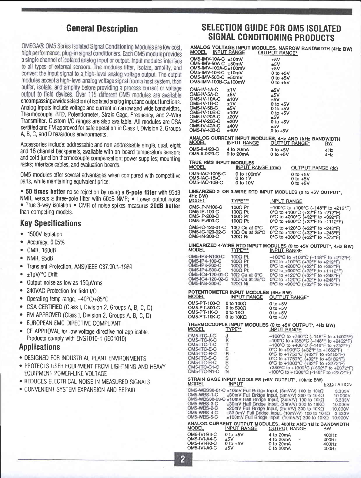
General
encompassingawide
Analog
inputs
Thermocouple,
Iransmitter.
certified
A, B,
C,
and
and
Accessories include:
16
and
channel backpanels,
and
racks;
0M5
parts,
.
NMR,
e
rhan
Key
o
o
.
.
o
.
.
.
o
.
o
'
.
junction
cold
interlace
modules
while maintaining
50 times beller noise
versus
True
3-uaY
competins moders
SpeCifiCatiOnS
1s00v
rsorarion
Accuracy,
160dB
CMR,
NMR,
95dB
Transient Protection,
tlpV/'C
0utput noise
240VAC Protection lor
Operating temp
cSA CERTIFIED
FM
APPRoVED
EUROPEAN
AppR0vAL for low
cE
Products
comply
Applications
o
DESIGNED
.
PROTECTS
EOUIPMENT
.
REDUCES
.
CONVENIENT SYSTEM
selection
include
voltage
RTD, Potentiometer,
Custom
FM
approved for
hazardous
D
ranges
U0
environments.
addressable
thermocouple
cables,
and
offer
severaladvantages
equivalent
a threepole
isolation
0'05%
Drift
as
EMC DIRECTIVE
FOR
USER EOUIPMENT
POWER-LINE
ELE0TRT0AL
filter
o
CMR
ANSil|EEE
low
1S0pVrms
as
field
-40.C/+g5.C
range,
(Class
I, Division
(Ctass
t, Division
voltage
with
ENG101G1
INDUSTRIAL
NorsE rN
EXPANSION AND
Descriplion
iso
lated
of
and
safe operation
available with
compensation;
evalualion
rejection
[0
VOLTAGE
analog
in narrow
current
Strain
Gage,
are also
available. Ail
in
non-addressable
and
on-boud
boards.
when
price:
by
using
wjth
noise
0f
C0MPLIANT
directive
PLANT
FROM LIGHTNING
NMft
OOOB
spikes measures
C37.90.1-1989
2,
Groups A,
2,
Groups A,
not
(tEC1010)
ENVIRONMENTS
MEASURED
REPAIR
inputand
and wide
Frequency,
Class l,
Division 2,
funclions.
output
bandwidths,
and 2-Wire
modules
are CSA
Groups
single, dual,
tempeiature sensors
power
supplies;
compared
a 6-pole liller with
:
fo*rfo_rlq,]lilii;
B,
c, D)
B,
c, Di
applicable.
AND
STGNALS
mounting
with
competitive
20tlB
Detler
HEA\Ti
SELECTION
SIGNAL
$IALOG
M@EL
OM$|MV-IOA€
OM$'|MV-SOA€
OM$|MV-100A€tl@mV
OM$IMV-I0B€
OMSIMV-SOB€
OM$lMV-1008€*1OOmV
OM$|V-IAC
OM$IV-SAC
OM$|V-1OA€
OM$|V-1BC
OMS-|V-SBC
OM$]V-1OBC
OM$|V-2OA€
OM$lV-2oB€
oM$tv-4oA€
OM$lV*4oB€
AllAl=OG
eight
gsdB LINEARIZED
MODEL
9M$ll-4r20-C
OM$llOl2GC
TRUE
MODEL
OMtlAGlO0B€
OM$IAGIB€
OM$|AAIOB€
ffi
olrr+rp-rurooc
3MllF-_Iffi
oM$lP60Gc
OM$1G120-01C
VoLTAGE
tNpur
CURRENT
RMS INPUT
2- oR s-wRE
3Mrir.lffi.
L|NEARTZED
MopEL
porENnoMETER
MoDEL
EMfFi:lffif
3illFT:I5f"
rHERMocoupLE
MoDEL
ffii
&wtRE
GAGE INPUr
GUIDE
FOR
OMs
CONDITIONING
INPUT
RANGE
11OmV
+SOmV
+1OmV
$0mV
*1V
tSV
110V
*1V
tSV
110V
*2OV
*:ZoV
t4ov
t4OV
INPUT
TNPUT
RANGE
4
to
zOmA
0 to
20rn/A
MODULES
INPUT
0 to
lOOmV
0
to tV
o
to 10V
RrD INPUr
rypE-.
pt
looo
iffi
F[
loori Pt
10O
Cu at
lsn",t,"
RTD tNpur
TypE"'
tNpur
MoDTJLEs
INPUT
RANGE
3 3
lffi
33;5P"
tNpur
TYPE"
MoDULEs
MoDULES
Mo^UJLES,
omui-
MODI LES.
MNGE
0"C O"C
25"c
{ F.Eqw
neruce;
*5V
t5V
t5V
0
to +5V
0 to +5V
0 to +5V
+5V
*5V
*5V
O
+5V
to
O
+5V
to
O
to +5V
t5V
O
to +5V
t5V
O
+5V
to
4Hz
AND ikHz BANDWTDTH
OrtrPur
O to +5V
0 to +SV
(nm)
rNpur
-loo.c
gs
0'c to +6oo"c
33ls
MqpgFs^(g.t9+5V
rNpUT
(4Hz
OLnPur
RANGE;
OUTPUT RANGE
0 to +5V
0
0
MoDULES
BANGE
to +100.c
llll3gs]lg:r
lo +120.C
ll33:8
RhNGE
Bw)
hANGE'
3lS i8V
33i3V
(o_to_+!V
lNPur
('5v
ourpur, 4Hz
RANGE
ourPur,
ISOLATED
PRODUCTS
BANDW|DTH (41-rz
-
+5V
to
+5V
to
(o
ro
i+32'F
(+32.F
i*i:r
lokHz
+sv orrrpur,
(-148.F
li i333:B
to +ttiz'F)
to +248"F)
g
i?#:?,
ourpup,
"u.*"rolo*
Bw)
EW
4Hz
4Hz
(dc)
to +2.12"F1
-
'
4Hz Bw)
Bw)
ANALOG
MoDEL
OM$lVl-844
OMFIVI-A44
OM$IVI-BGC
OM$IVI-AGC
CURRENT
OUTPUT
INPUT
RANGE oL'TPL'T
O
+5V
to
*5V
0 to +5V
*5V
MODULES.
4
to 20rnA
4
to 20rnA
O to
20rnA
0 to
2OrnA
4ooHz
AND lkHz BANDWIDTH
BANGE
BW
4OOHz
4OOHz
400H2
4@Hz
Page 5
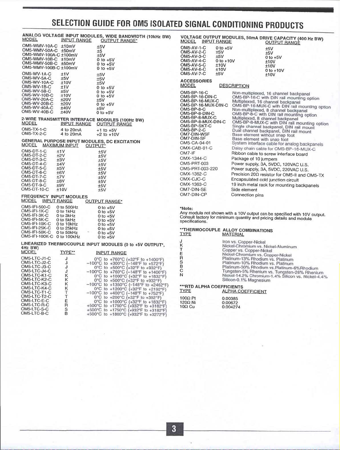
SELECTION
4.ryALOG
MODEL
oMs-WMV-loA-C
OM5-WMV-50A-C
OM5-WMV-loOA-C
OM5-WMV-1OB-C
OM5-WMV-508-C
OM5-WMV-loOB-C
oM5-WV-1A-C
oM5-WV-5A-C
oM5-WV-1oA-C
oMs-wv-l8-c
OM5-WV-58-C +5V
oM5-WV-108-C +10v
oM5-WV-2oA-C
oM5-WV-20B-C +20V
oMs-wv-4oA-C
oM5-WV-408-C
2:W!RE
MODEL
OM5-TX-1-C
OMs-TX-2-C
GENERAL
MODEL
OMs-DT-I-C
oMs-DT-2-c
OMs-DT-3-C
oM5-DT-4-C +4V
OM5-DT-5-C
oMs-DT-6-C
oM5-DT-7-C
oMs-DT-8-C +8V
oM5-DT-9-C +9V
OM5-DT-10-C
FREOUENCY
MODEL
OM5-|F|-5OO-C
OMS-lFl-1K-C
OM5-|F|-3K-C
OM5-|F|-5K-C
OM5-|F|-1OK-C
OMs-lF|-25K-C
OM5-|F|-5OK-C
OM5-|F|-1OOK-C
LINEARIZED
4Hz BW)
MODEL
oM5-LTC-J1-C
oM5-LTC-J2C
oMs-LTC-J3-C
oMs-LTC-J4-C
OM5.LTC.KI-C
oM5-LTC-K2-C
oMs-LTC-K3-C
oM5-LTC-K4-C
oM5-LTC-T1-C
oM5-LTC-T2-C
oMs-LTC-E-C
oM5-LTC-R-C
OM'LTC.S.C
oM5-LTC-B-C
VoLTAGE
TRANSMTTTER
PURPOSE
MAXIMUM
INPUTRANGE
INPUT
ttomV
rSOmV
11OomV
rtomv
+sOmV
tto0mV
+1V
rsv
110V
i1V
+20v
r40v
+40V
INPUT
4
to
4
to 2OmA
INPUT
+lV
!2V
+3V
+5V
r6V
!7V
+10V
INPUT
O to 50OHz
O
to
O
3kHz
to
O
skHz
to
O
lOkHz
to
25kHz
0 to
O
SOkHz
to
O
lOOkHz
to
THERMOCOUPLE
TYPE'-
J
J
J
J
K
K
K
K
T
T
E
R
5
B
INPUT
MopuLEs,
RANGE
iNT-ERFACE
BANGE
2OmA
INPUT
MODULES,
OUTPUT'-
MODULES
lkHz
OUTPUTRANGET
tNpUT
GUIDE
t5V
15
+5V
O
0 to
0 to
15V
t5v
+5V
0 to
O to
O to +5V
r5V
0 to +5V
r5V
O to +5V
MODULES (tooHz
OUTPUT
+1 to
+2
+SV
rsv
+SV
+5V
+5V
rsv
tsv
rsv
JsV
iSV
O to +5V
O to
O
O
O
O
O
0 to +5V
TNPUT
FOR
wlDE
+5V
+5V
+5V
+5V
+SV
to +tOV
DC
EXCITATION
+5V
+5V
to
+5V
to
to +5V
to +5V
to +5V
RANGE
BANDWIDTH
RANGE
OUTPUThAfEE;
to +5V
MODULES (0
OMs
BW)
+5V
to
ISOLATED
(1okHz
BW)
OUTPUT.,
VOLTAGE
MODEL
OM5-AV-1-C
oM5-AV-2-C
oMs-AV-s-C
OM5-AV-4-C
oM5-AV-5-C
oM5-AV-6-C
oM5-AV-7-C
ACCESSORTES
MODEL
oM5-BP-16-C
oM5-BP-16-DINC
OM5-BP-16.MUX.C
OM5-BP-16.MUX-DIN-C
oM5-BP-8-C
oM5-BP-8-DrN-C
OM5.BP-8-MUX.C
OMs-8P.8-MUX-DIN.C
OMs.BP.SKT-C
oM5-BP-2-C
OM7-DIN-WSF
OM7-DIN-SF
oM5-CA-04-01
OMX-CAB-01-C
oM7-tF
oMX-1344-C
oM5-PRT-003
oM5-PRT-003-220
oMX-1362-C
OMX.CJC-C
oMX-1363-C
OM7-DIN-SE
OM7-DIN-CP
'Note:
Any
uonsu[
specifications.
.'THERMOCOUPLE
TYPE
J
K
T
E
R
S
B
c
N
."RTD
ryPE
100c)
120cr
10r)
SIGNAL
module
ALPHA
Pt
Ni
Cu
CONDITIONING
OUTPUT
INPUT RANGE
0
rsv
isv
O to
r10V
rlOV
+5V
not.shown
ladory tor
mtntmum
COEFFIC]ENTS
MoDULES,
to +5V
+10V
DESCRIPTION
wirh
ALLOY
MATERIAL
ALPHA
o.oo385
o.00672
o.oo4274
SomA
Ribbon
cable
Package
Power
supply,
Power
supply,
Precision
Encapsulated
19
inch
metat
Side
element
Connection pins
a 1 0v
output
quantity
COMBINATIONS
COEFFICIENT
PRODUCTS
DRIVE
CApACtTy
oUTPUT
t5V
r5V
0
+5V
to
r10v
il0v
0
+10V
to
t10v
to
screw interface
of 10
lumpers
3A,
sVDC, 12OVAC
3A,
20O resistor
SVDC,
junction
cold
rack
for
can
be
and pricing
for
mounting
specified
details
(4Oo
AANGL
board
220VAC
OMS-ll
and
circuit
backpanels
with
and
module
- - ..-
Hz BW)
U.S.
U.S.
OMS-TX
1oV
_
..,
outout.
Page 6
@"9ce
OMS.IMU/TU
Analog
FEATURES
O ACCEPTS
O HIGH
o 1500Vrms
O
ANSI/IEEE
. INPUT
160d8
o
a 95dB NMR
o
i0.05%
.
fr.02%
o
tlpVfC
O
CSA
O MIX
MILLIVOLT
LEVEL
VOLTAGE
TMNSFORMER
C37.90.1
PROTECTED TO
cMR
AT
60Hz,90dB at
AccuMcY.
LINEARITY
DRlff
CERTIFIED,
AND MATCH
Uoltage
AND
VOLTAGE
OUTPUTS
|S0LATION
-1
989
TMNSIENT
24OVAC
FM
APPROVED,
OMs TYPES
CONTINUOUS
50Hz
CE COMPLIANT
ON BACKPANELS
Input
LEVEL
SIGNALS
PROTECTION
Modules,
lfarrow
DESCRIPTION
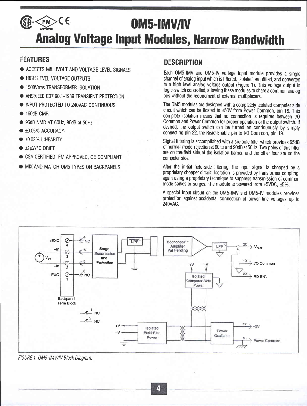
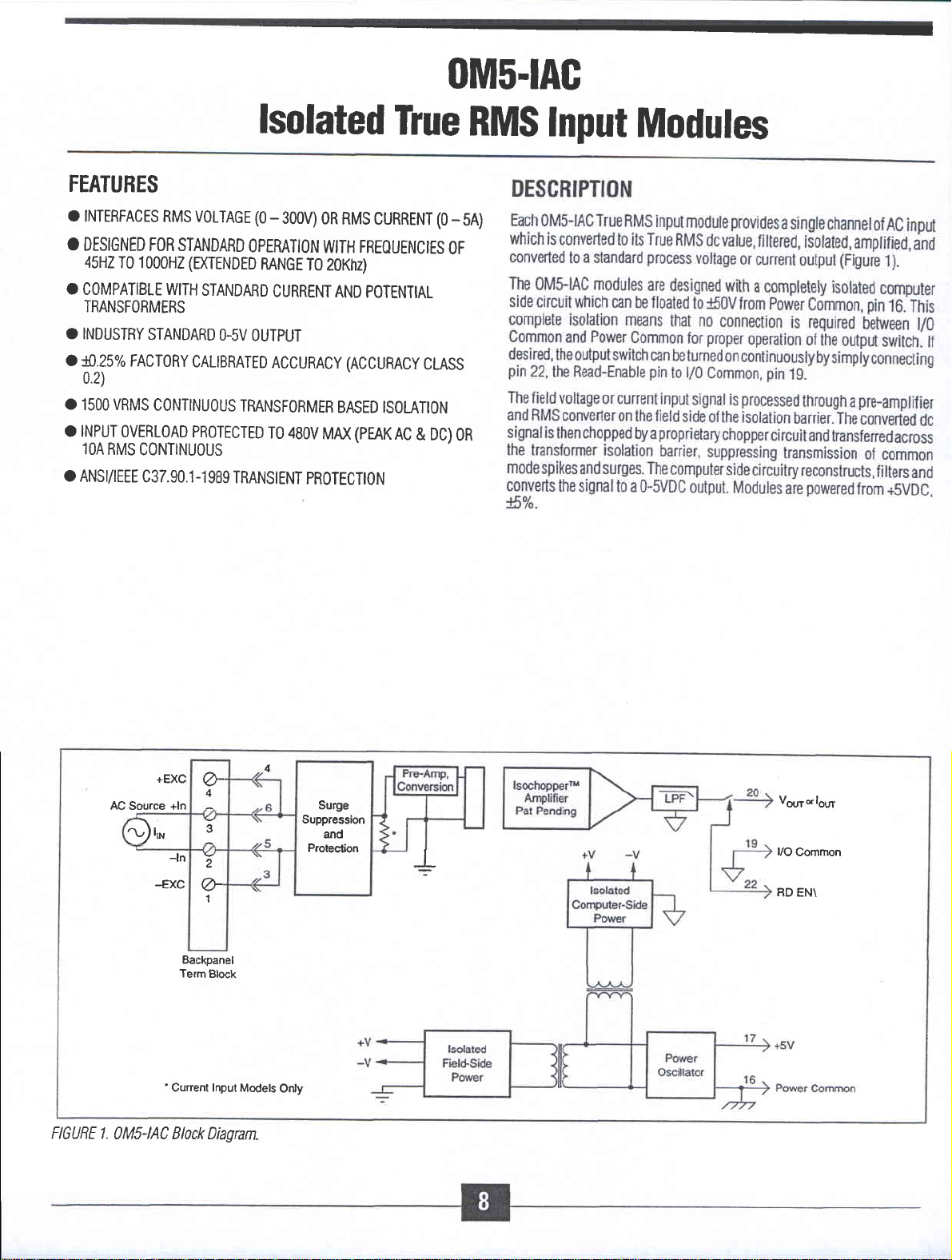
OMS-|MV
Each
channel of analog input
high level
to a
logic-switch
without
bus
The 0M5
circuit which
complete
Common and Power
desired,
connecting
Signal
of normal-mode+ejection
are.on lhe,field
computer side.
After the
proprietary
again using a
mode spikes
A
protection
240VAC.
-,the
filtering
special
and 0M5-lV voltage
analog
controlled,
the requirement
modules
isolation
initial field-side
input
are
can be floated
means
Common for
output
pin
chopper
against
switch can
22, the
is
accomplished
side
of the
circuit.
proprietary
0r
surges. The module
circuit
accidental
Bandwidth
input
which is
voltage output
allowing
designed with
Read-Enable
on
filtered, isolated,
these modules
of external
to r50V
that no
at 60Hz
isolation
filtering,
lsolation
technique
the
connection
proper
be
turned
pin
with
a
and
barrier,
the input
is
to suppress transmission
is
OMS-|MV
connection
(Figure
multiplexers.
a completely
from
six-pole
90dB at
provided
powered
module
Power Common,
operation
on
to l/0 Common,
50H2.
and the
and
0M5-tV modules
power-line
of
provides
amplified,
1).
This voltage
to share
isolated
is required
of
continuously
filter
signat is
by
lrom
and
a common
computer
the output
pin
provides
which
poles
Two
other four
chopped
transformer
+SVDC,
voltages
a single
convertid
output is
analog
pin
between
side
16. This
switch. lf
by
simply
19.
95dB
of
filter
this
are
on
by a
coupling,
of
common
r5%.
provides
up
l/O
the
to
3u*
FIGURE
1.
+EXC
-EXC
G
4
+ln
3
-ln
2
U
Backpanel
Term Block
1
x
-<j
-€
1Ms-lMVlV Block Diagran.
Surge
and
Protection
nrc
""
+V
lll
I
Vour
l/O
RD
Common
EN\
Page 7
SPECIFICATI0NS
rypinr
ar T^ = 1r5"s
and
power.
+5V
Module
lnput
Range
Input
Bias
Input Resistance
Inpul
CMV, Input
CMR
NMR
AccunaqYttl
Nonlinearity
Stability
Noise
Bandwidth,
Response
0utput Range
Output
0utout
0utput Selection Time
0utput
0utput
Power
Power
Power
Mchanical
Environmental
Emissions
lmmunity
Cunent
Normal
Power
Off
Overload
Protection
Continuous
Tnnsient
to
Conlinuous
Transienl
Input
Outpul
Gain
Input,
0utput, 100kHz
(to
Mu
Min
Mar
Input
Openating Temp.
Stonge Temp.
Relative
output
(50H2
or 60Hz)
ofisel
0ftset
0.1
10Hz
to
-3dB
Time,90%
Resistance
Protec{ion
tlmv
ot Vou
Current Limit
Enable
Conkol
Logic'0"
"1"
Logic
Logic'1'
Supply Voltage
Supply
Supply
'0',
Current,
Currenl
Sensitivity
Dimensions
Range
Humidity
Span
)
'1"
Range
0M5-tMV
t10mv
$.5nA
50MO
40tc,
4okf,i
240Vrns
ANSt/rEEE
ANSTnEEE
95dB at
:0.05%
C37.90.1-1989
1500Vms
C37.90.1{989
160d8
60Ha
Span
$qry Rn(,'l0.05%(VzP)
J0.02% Span
rlpvfc
t204trc
*25ppm/.C
02pVrms
2@pVms
4Hz
0.2s
r5V.
0V to
Conlinuous
'Qs
50(|
at
C- = 0 lo
$mA
+0.8V
+2.4Y
+36V
0.5r4
Short to
+SVDC
30mA
f2pvl% RTIta
2.28'x2.26'x 0.60'(58mm
-40.C
to +85.C
-40oC
to +85.C
95% Noncondensing
Group 1,
Class A
Group
EN50081{,
ISM
EN50082-1,
0 to
ISM
lo tlmmv
mu
mu
g0dB
at 50Hz
+5V
Ground
2000pF
l5%
x
57mm x 15mm)
(Radiated,
1,
Clas A
Conducted)
(ESO,
RF,
EFT)
g).05%
t1V
650kfi
650Kr
650Kr
Span
{.2mV
90pVfC
r50ppm/.C
2pV.rms
i200pV/%
0M5-tv
to #0V
r0.05nA
(minimum)
(minimum)
(minimum)
RTP'$.05%(V,G1
RTIa
'
specilication
Sarne
(1)
NOTES:
hysteresis and
(2)
(3)
in 0V
Includes
=
RTI
ftsfgrcnced
is
V,
lhe input voltage
outout.
as 0M5-lMV.
nonlinearity.
repeatabi
lity.
to in'ut.
that results
ORDERING
INFORMATION
MODEL
0M5rMV-1oA-C
0MrrMV-soA-C
0M5-rMV-100A-C
OMFIMV-1OB-C
0M5-tMV-s08-C
0M5-rMV-1008-C
0M5-rv-1A-C
0Ms{v-5A-C
0Msrv-1oA-c
0M$rv-18-c
OMFIV-sB-C
0Milv-108-c
0M5-rv-20A-c
0M5-rv-z08-c
0M5-rv-4oA-c
0M5-rv-408-c
INPUT
-1OmV
-50mV
-10ffnV
-1()mV
to
-50mV
to
-100mV
to
-1V
to
-5V
1o
-10V
to
-1V
to
-5V
1o
-10V
to
-20V
to
-20V
to
-40V
lo
-40V
to
RANGE
+1OmV
to
+50mV
to
+100mV
to
+1OmV
+50mV
+100mV
+1V
+5V
+10V
+1V
+5V
+10V
+20V
+20V
+{0V
+40V
OUTPUT
RANGE
-5V
to +5V
-5V
+5V
lo
-5V
+5V
to
0V
+5V
to
0V lo +5V
0V to +5V
-5V
+5V
to
-5V
to +5V
-5V
to +5V
0V
+5V
10
+5V
0V to
0V
+5V
to
-5V
+5V
to
+5V
0V to
-5V
+5V
to
0Vto +5V
Page 8
@"€>c€
0M5-ll
FEATURES
O ACCEPTS
O
HIGH
O l5OOVrms
O
ANS/IEEE
O INPUT
o 160d8
o
95dB
o
10.0570 ACCURACY
e
fr.lLo/o LINEARITY
O
CSA
O
MIX AND MATCH
MILLIAMP
LEVEL VOLTAGE
TRANSFORMER
C37.90.1-1989
PROTECTED
cMR
NMR
AT
60H2,
CERTIFIED, FM
LEVEL
SIGNALS
OUTPUTS
ISOLATION
TRANSIENT
TO
24OVAC
90rtB AT
APPROVED,
OMs
50Hz
ryPES
ON BACKPANELS
Analog
PROTECTION
CONTINUOUS
CE
COMPLIANT
Gurrent
Input
Modules
Backpanel
Term Block
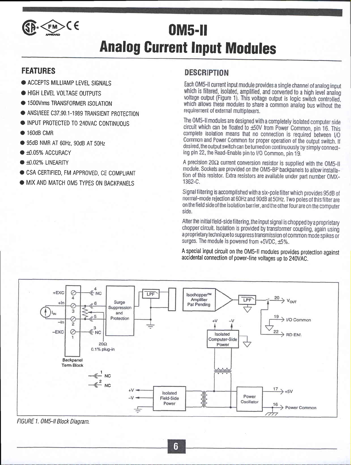
FIGURE 1. 0M5-llBlock
Diaoran.
_<j
<4
*"
""
A
special input
accidental
connection
circuit on
power-line
of
the
0M5-ll modules
voltages
provides
up
protection
to 240VAC.
against
Page 9
S PEC I Fl CATI 0 N S Typicat
Module
Range
lnpul
Resistor
Inpui
Value
Accuncy
Stability
Proteclion
Input
Continuous
Transient
Input
CMV,
CMR
NMR
AccuncY'l
Nonlinearity
Stability
Noise
Bandwidth,
Response
0utput
0utput
output
Output
output
output
Input Cunent,
Power
Power Supply Cunent
Power
Mechanical Dimensions
Environmenhl
Operating
Stonge
Relative Humidity
Emissions
lmmunity
to Output
Continuous
Transient
(50H2
or 60Hz)
Input offset
0ffset
Output
Gain
Input,0.1H2 to
100kHz
Output,
-3dB
Time,
90% Span
Bange
Resistance
Protection
Selection Time
(to
Mu
Min Logic
Max Logic'1"
V'n)
tlmv of
Current Limit
Enable Control
Logic'0'
'1"
'0,1"
Voltage
Supply
Supply Sensilivity
Temp. Range
Temp.
Range
1OHz
T^ = +25"C
at
EN50081-1,
power.
and +5V
0M5-rl
()mA
to 20mA
or
4mA
20.00(r
10.1%
iloppmfc
240vrms max
ANSt/rEEE
ANSt/EEE
95dB
$.05% span
Continuous
6Is at Cbd = 0
C37.90.1-1989
1500Vrms
C37.90.1-1989
160d8
at 60H2.
90dB at 50Hz
$.05%
10.02% Span
i50nA/.C
i201tYfC
95ppmfC
l0nArms
2O0pVrms
4Hz
0.2s
+5V
0 to
50rl
Short
lo 2000pF
+8mA
+0.8V
+2.4Y
+36V
0.5pA
+5VDC
15%
3OmA
+20pV/% RTlto
2.28'x 226'x
(58mmx57mmx15mm)
-40'C
+85oC
to
-40'C
1.
Group
ISM
Group 1, Clas A
to +85"C
Class
0 to 95% Noncondensing
ISM
EN50082-1,
lo 20mA
mu
(1,(,)
to Gnd
0.60'
(Radiated,
A
(ESD,
Conducted)
RF,
EFT)
(1)
NoTE
Includes nonlinearity,
results
in
0V
ORDERING
(3)
output.
RTI = Referenced
INFORMATION
MODET
oMs-il4/20-c
oM5-il-0/20-c
hysteresis
and
input.
to
RANGE
INPUT
4mAto 20mA
OmAto 20mA
repeatability. (2)
I,is
input
the
OUTPUT
0V to +5V
0V to +5V
that
cunent
RANGE BANDWIDTH
4Hz
4Hz
Page 10
0M5-lAC
FEATURES
o
TNTERFACES
O
DESIGNED FOR
45HZ
O
COMPATIBLE WITH
TRANSFORMERS
. INDUSTRY
o
fi.25yo FACToRy
0.2)
O
15OO VRMS
o lNpuT
1OA
RMS
O
ANS/IEEE
RMS VoLTAGE
STANDARD
1000H2 (EXTENDED
T0
STANDARD
CONTINUOUS
0VERLoAD PR0TECTED
CONTINUOUS
C37.90.1-1989
lsolated
-
(0
300V)
OPEMTION
MNGE
STANDABD
O-sV
CALTBRATED
CURRENT
OUTPUT
ACCURACY (ACCURACY
TMNSFORMEH
T0 480V
TRANSIENT
True
0R
RMS CURRENT (0
FREOUENCIES
WITH
T0 20Khz)
AND
POTENTIAL
BASED ISOLATION
(PEAK
MM
PROTECTION
AC
& DC)
RMS
_
5A)
OF
CLASS
0R
Input
Modules
FIGURE 1.
+EXC
U
4
Source
9,,n
-EXC
+ln
-ln
Backpanel
Term
'Cunenl
<J
J
2
6
1
Block
Input Models
AC
)MS-|AC Block Diaoran.
4
Onty
Surge
Suppression
and
Protection
Vsura
l6ur
l/O
Common
I
RD EN\
Page 11
SPEC|
FICATI0NS
Input
Signal
Range
Shndard Freguency
E{ended
Frequenry
|mpedance
Coupling
Proteclion(t)
Continuous
Tnansient
0utput
Signal Range
Cunent
Limit
Voltage
Limit
Rcistance
Protection
Ripple
AccuracY4s)
Sinusoid
Non-Sinusoid
Crest
Crcst Factor
Crest
Crest Factor= 4 to
Vs. Tempenture
lsolation
Input
0utout to Power
Continuous
Noise
and
50/60
Hz
45Hz
to lkHz
lkHz
to 20kHz
Factor = 1
=
2 to
=
Factor
3 to 4
(Common
t0 output,
Continuous
Transient
Ran
Range
(100Khz)
to
2
3
5
Mode)
lnput
to Power
Typicat
ge
at T^= +25"C
and
100mV
1 MOrl%
shunred
0.05c)11%
480V
ANS|/EEE
Continuous
{).25%
10.75%
r0.05% Reading
10.15%
r0.30%
$.40% Reading
ANSr/rEEE
power.
+5V
to 10V
rms,
0 to
45Hz
to 1000H2
lkHz
by 10sF
(Peak
C37.90.1-1989
G5V
8mA
n18v
5ocl
Short
0.025Yo
1025%
Reading Additional
Reading Additional
Reading
Reading Additional
t100ppm/.C
l5@Vrms max
C37.90.1
50Vdc max
SA rms
t0
20kHz
(-01
-07)
(-06,
AC
AC
&
DC)
to
Ground
Span rms
Span
Factor
Factor
Addilional
Additional
Additional
-1989
Error
Eror
Enor
thru
Enor
-05),
ORDERING
INFORMATION
UIODET
0M5-|AC-1008-C
0M5-rAC-18-C
0M5-rAC-108-C
INPUT*
(rms)
G100mV
0-1v
0-10v
0UTPUT.
(dc)
0-5v
0-5v
0-5v
Response
Selection Time
Voltage
Mu
Min / Max
Current,
Environmental
Operating Temp. Range
Stonge Temp. Range
Relative Humidity
Emissions
lmmunity
Dimensions
NOTE:
(1)
Module
accordance with
(2)
Al standard
(3)
For1G100%ratedspan.Addanadditional0_25%enorfortr10%Spanmeasuremenh.
Accuracy
inaccuracy (if
(0
Time
to 99%)
Logic'0'
'1-
Logic
"0,1'
rating
only. Backpanel
required
tactory
601-lz
includes nonlinearity,
used).
6.hS@CLoAo=0t02000pF
+7.5Vdc
(Loop
Voltage - 14)
EN50081-1,
EN50082-1,
2.28' x226'
connctor rating
ufety requirements.
calibntion. Consult lactory
hysteresis
0 lo
ISM
Group
ISM
x
may
differ- use
lor
and repeatability
+0.8V
+2-4V
l+3N
0.srtA
min, +26Vdc
(Loop
/
+SVDC
l5%
30mA
!200p!n/%
-40'C
to +85'C
-40'
c t0 +85'c
noncondensing
90%
1,
Class A
1,
Group
Ctass A
(58mm
0.60'
calibration
x
the
at olher trequencies.
but not
s0urce
max
Current)
(Radiated,
(ESD,
57mm
x 15mm)
lowest
of
or exlemal
Conducted)
RF, EFI)
the two in
shunt
'
Modules can
ordering delails
be
ordered
and
socifications.
with other inpuvoutput
nanges. Consult
lactory
for
Page 12
@.9ce
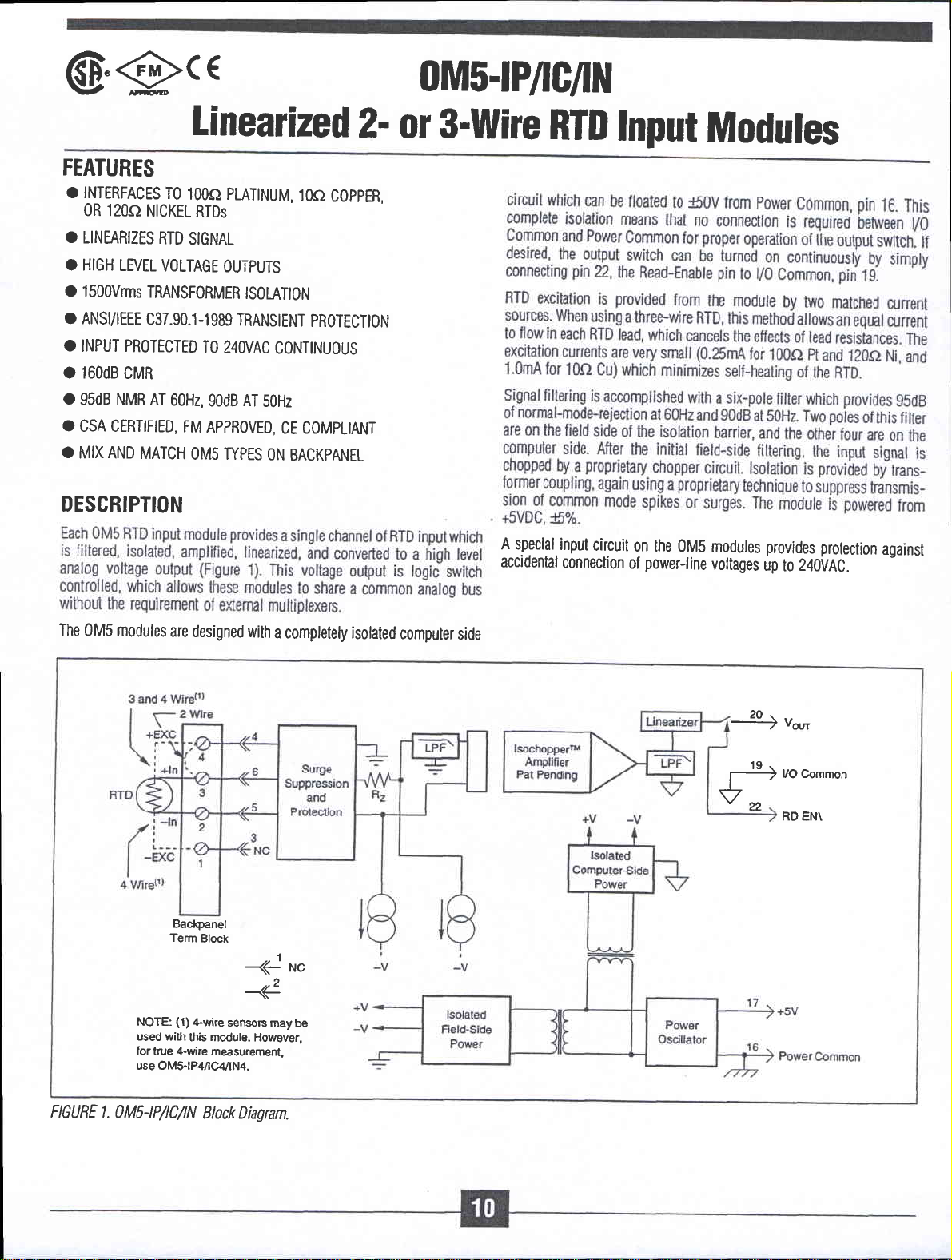
0M5-tPlc/t1{
Linearized
FEATURES
O INTERFACES
0R 120o
.
LINEARIZES
O HIGH
O
lSOOVrms
O ANSI/IEEE
O
INPUT PROTECTED
o 160dB
o
O
O
NMR
95dB
CSA CERTIFIED,
MIX AND
DESCRIPTION
TO
1OOO PLATINUM,
NICKEL
LEVEL
TMNSFORMER
C37.90.1
cMR
MATCH
RTDs
RTD
SIGNAL
VOLTAGE
-1
989
TO
AT
60H2,
90dB
FM
APPROVED,
OMs IYPES
1OO
OUTPUTS
ISOLATION
TRANS
IENT
24OVAC
CONTINUOUS
AT
50Hz
CE COMPLIANT
ON
BACKPANEL
2-
oJ 3-wire
COPPER,
PROTECTION
RTD
A special
accidental
input
connection
Input
circuit
on the
power-line
of
Modules
0M5
modules
voltages
provides
up
240VAC.
to
prolection
against
The
0M5 modules
are
designed
Baclganet
Term
(1)
NOTE:
used v/ith
for
use OMs-lP4IC4/1N4.
+wire
this module. However,
4-wire
true
with
Block
<_
sensors may
measurement,
a completely
I
Nc
tt2
be
isolated
computer
side
j)
-5
v^^
?2
uo-
uocommon
RD
EN\
FIGURE 1.
1M1-lPlC/lN
Block Diagnn.
Page 13
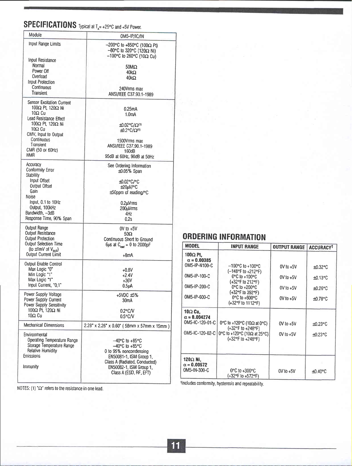
SPECIFICATI0NS
Module
Input
Range
Limits
Input Resistance
Nomd
Power
Off
0verload
Protection
Input
Continuous
Transient
Sensor Excitation
100c}
10O
Resistance
Lead
100f2
10O
Cu
Input
CMV,
Continuous
Transienl
(50
CMR
NMR
Accuracy
Conformity
Stability
Input
0flset
0utpul 0ffset
Gain
Noise
Input,0.1
outpul, 100kHz
Bandwidth,
Response
Range
0utput
Resistance
0utput
Protection
Output
ouhut Selection Time
(to
ilmv
0utout Curent
0utput Enable
Mu Logic
Min Logic
Mu Logic
Input
Cunent,
Power
Supply Voltage
Power
Supply
Power
Supply
Pt,
1000
10cr
cu
Mechanical
Environfiental
Operating Temperalure
Storage
Relative
Emissions
lmmunity
'O'
(1)
NoTES:
Current
Pt, 120c1
Cu
Temperature
Humidity
Ni
Effect
Pt, 1200
Ni
to 0utput
or 60Hz)
Enor
to 10flz
-3dB
Time,
90%
ot VouI)
Limit
Control
'0'
"1"
'1"
"0,1"
Cunent
Sensitivity
120c2
Ni
Dimensions
refers
l0 the resistance
Span
Range
Range
lypicat
ar To= +25oC
2.28'x2.26'x
in
lead.
one
power.
+SV
and
0M5-rP/C/N
-2@"C
-100'C
-80'C
+850.C
to
to 320.C
260.C
to
000C2
(120f,l
(10O
50MO
4oko
40krr
240vrms max
ANSI/EEE
ANSr/EEE
95dB
See
150ppm
Continuous
6;s at C* = 0 to 2000pF
C37.90.1-1989
0.25mA
1.0mA
$.02.c/o(')
{.2clattt
1500vrms
at 60H2, 90dB
0rdering
10.05%
+5VDC l5%
max
C37.90.1-1989
160d8
Information
Span
fi.02cfc
90FV/"C
reading/"C
of
02pVrms
2fi)pVrms
4Hz
02s
+5V
0V to
50f2
Short to
Ground
+8mA
+0.8V
+2.4V
+36V
0.stA
30mA
at
50Hz
02,cN
0.5.c/v
(58mm
0.60'
-40'C
-40oC
to
0
95%
EN50m1-1,ISM Group
(Radialed,
Class A
EN50082-1, ISM Group
Class A
x
57mm
+85oC
to
+85"C
lo
noncondensing
Conducted)
(ESO,
RF,
EFf)
pt)
Ni)
Cu)
x 15mm
1,
1,
ORDERING
MODET
100c)
a = 0.00385
0M5-tP-N10&C
0M5-tP-10GC
oMtsrP-2otrc
0M5-rP-6otrC
1|lf,)
cu,
a=0.004274
0M5-rc-12S.01-C
)
0M5JC-12G02-C
120cl
a = 0.00672
0MsrN-3oGc
rlrpludes
n,
lti,
conformity,
hysteresis
INFORMATION
II'IPUT
BANGE
-100'C
to +100.C
(-148"F
(+32'Fto
0'C to +120"C
(+32'F
()oC
to +120'C
(+32.F
{+32"F to +572'F)
+212.F)
to
00c
+1
t0
(+32"F
(+32'F
0"c
00"c
to
212"F)
OoC
+200oC
lo
to
392"F)
0"C
lo +600oC
1112.F)
(10O
at
to +248"F)
(l0O
at
+249"F)
to
+300"c
t0
and repeatability.
0.C)
25"C)
OITIPUT
RANGE
0V to +5V
0V
to +5V
0V to +5V
0V to +5V
0V to +5V
0V
+5V
to
0Vto +5V
ACCURACY'
10.32"C
10.13.C
10.26.C
g).78.C
i0.23.C
{.23C
10.40"c
Page 14

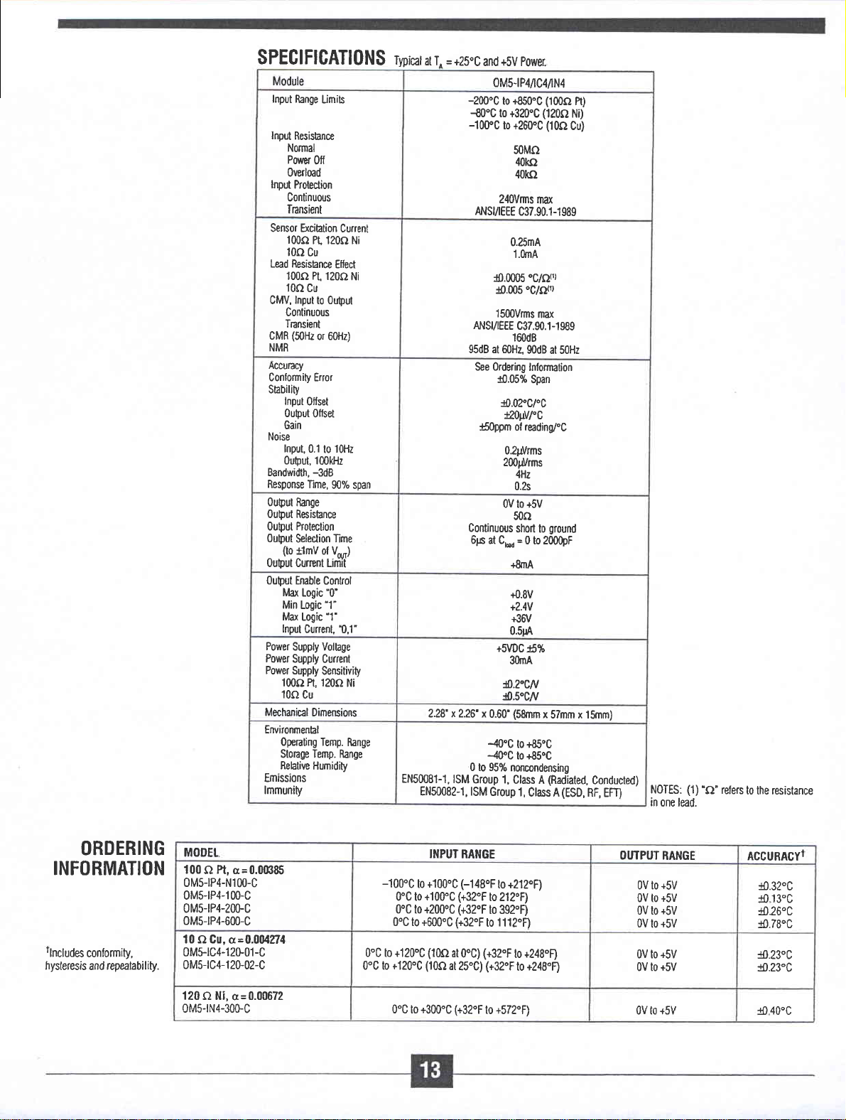
@.9ce
0M5-tP4/tG4/tN4
FEATURES
O
INTERFACES
0R 120cl NICKEL
. TRUE
O
LINEARIZES RTD
O HIGH
O
lSOOVrms
O
ANSI/IEEE
O INPUT
o 160d8
O
95dB NMR
O
CSA CERTIFIED, FM
O MIX
AND
DESCRIPTION
TO
1OOO PLATINUM,
RTDs
4-WIRE
LEVEL
INPUT
SIGNAL
VOLTAGE
TRANSFORMER
C37.90.1-1989
PROTECTED
cMR
AT
MATCH
TO
gOdB
6OHZ,
APPROVED,
OMs TYPES
Linearized
1OO
COPPER,
OUTPUT
ISOLATION
TRANSIENT
24OVAC
AT
PROTECTION
CONTINUOUS
sOHZ
CE COMPLIANT
ON
BACKPANEL
4-Wire
RTD
RTD
The
excitation
two input
the input
independent
for 100
heating
Signal filtering
of normal-mode-rejection
are on
Input
excitation
Cr Pt
of the RTD.
the field
provided
is
cunent is
signal
measuring
signal
leads, which
of lead resistance.
and 120 O Ni
is
accomplished
side of
Modules
lrom
available
leads.
The
and 1.0
at
60Hz and
isolation
the
the
module
by a
on two leads
The
allows
excitation
mA for 10A
with
a
90dB at
barrier,
which
excilation
RTD measurement
current is
Cu) which-minimiies
six-pole filter which
50H2. Two
and
precision
cunent
the other four
current
are
separate
does not
very
snull
provides
poles
to
of
source.
from
the
flow
in
be totally
(0.25mA
setf-
95dB
fitter
this
are
on
the
3-Wire RTD
equal lead resistances,
lead resistances.
module
RTD
4w..e
RTD
provides
while
+EXC
+ln
)
--tn
-EXC
Backpanel
Term
+
Yr
4
3
2
Block
lead
resistance
the 4-wire
3
<d
-<3
modules
""
""
compensation,
do not require
:]-l
Surge
Suppression
and
Protection
but requires
matched
rpr-l
I
l=
I
A special input
power-line
voltages
provides
circuit
up to 240VAC.
protection
against
accidental
vow
l/O
Common
RD EN\
connection
of
FIGURE l.
0M5-lP4/lC4/lN4
Block Diagnm.
Page 15
SPECIFICATIONS
Typical
Module
Input
Range
Limih
Input
Resishnce
Normal
Pourer
Off
Overload
Input
Prohction
Continuous
Transient
Sensor Excihtion
100cl
10O
Lead Resisbnce
1000
10O
lnput
CMV,
Continuous
Transient
(501-lz
CMR
NMR
Accurircy
Conformity Error
Shbility
Input
0uput
Gain
Noise
Input,0.1
0ubut, 100kllz
Bandwidth,
Response Time,
Pt, 120fi Ni
Cu
Eflect
120cr
n,
Cu
to OuSut
or 60flz)
0ffset
Otfset
10Hz
to
-3dB
90% span
Curent
Ni
0uFut Range
Ouput Resishnce
Protection
ouFut
0uput
(to
Time
Seleclion
tlmv of V"n)
0uDut Curent Linii[
0uput Eruble
Power
Power
Power
Mechanical
Environmenbl
Bnissions
lmmunity
Conkol
lilax
Min
[4ax
Input
"0"
Logic
"1"
Logic
"1'
Logic
Cunent, 0,1"
Supply Volhge
Supply Current
Supply
Sensitivity
100rl Pr, 120r)
10O
Cu
Openting Temp.
Stonge Temp. Range
Rebtive
Ni
Dimemions
Range
Humidity
EN50081-1,
EN50082-1, ISM
at Ta = +25"C
and
-200'C
+0'C lo +320'C
-10trC
ANSyTEEE
Al,rsr/rEEE
95dB at 60Ha
See 0rdering
l5oppm ol reading/"C
Continuous
66 at C*
2.28'x2.26'x
-40.C
-.40pC
0 to 95%
ISM
Group 1,
+5V
Power.
0M5-tP4/tC4/lN4
(100cr
+850"C
lo
(120fi
to +250"C
(104
50MO
40ko
40ko
240Vms
max
C37.90.1-1989
0.25mA
1.0mA
10.0005'c/or)
$.m5.c/o{r}
1500vrms
rnax
-1
c37.90.1
160d8
989
90dB at 50Hz
Inlomation
:0.05%
Span
10.02.c/"c
f20pV/'C
0.2pilrms
200prms
4Hz
0.2s
0V to +5V
50r2
ground
short to
=
0 to 2000pF
+8.n4
+0.8V
+2.4V
+36V
0.$A
+SVDC
$%
3()tnA
{.z"CN
$.5'C/V
0.60'(58mm
Group
x
57mm x 15mm)
to +85.C
to +85.C
noncondensing
(Radiated,
Class A
1,
Class A(ESD, RF,
Pt)
Ni)
Cu)
Conducted)
EFI)
(1)
NOTES:
in
one leacl.
"f2'reters
t0 the resistance
ORDERING
INFORMATION
rlncludes
conformity,
hysteresis
repeatability.
and
MODEI
100
O n, a=0.00385
0M5-rP4-N100-C
0M5-rP4-100-C
0M5-tP4-2oOC
0M5-rP4-60GC
10 a cu,
a=0.00/,n4
0M$rc4{2G01-C
0M5-rc4-12S02-C
120
o Ni,
0M5-rN4-30GC
c=0.00672
-100'C
to
0'C to
+100'C
+100'C
0'C to +20fC
0'C to +600'C
0"C to +120"C
0'C to
(10O
(l0O
+120oC
+300'C
0'C lo
INPUT
(+32'F
(+32'F
(+32'F
at
at
25'C)
(+32'F
RANGE
(-148'F
to +212.F)
to 212'F)
to 392"F)
to 1 1
(+32'F
0'C)
(+32'F
+572'F)
to
12.F)
+248"F)
to
+248"F)
to
OIffPUT
0V to
0V lo
0V to
0V
to
0V to
0V to
0V to +5V
RANGE
+5V
+5V
+5V
+5V
+5V
+5V
ACCURACYI
10.32"C
13.C
l0
$26.C
10.78.C
g).23"C
10.23"C
40.c
l0
Page 16
@.9ce
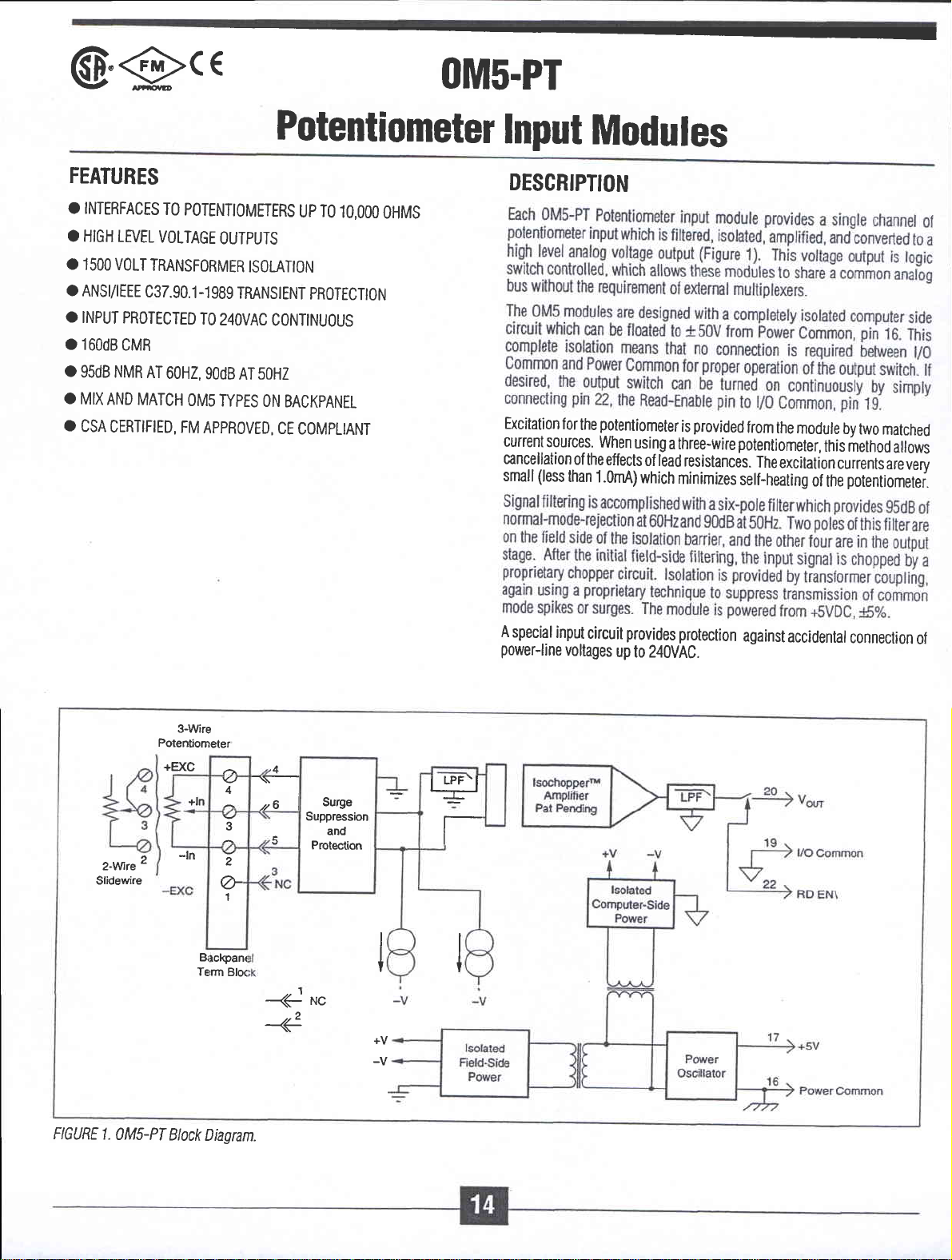
OM5.PT
FEATURES
O INTERFACES
O
HIGH LEVEL
. 15OO
o
ANSr/rEEE
O
INPUT
o 160d8
O
95dB NMR
O
MIX
AND
O
CSA
CERTIFIED,
TO
VOLTAGE
VOLT
TRANSFORMER
C37.90.1
PROTECTED
cMR
AT
6OHZ,
MATCH
FM
Potentiometer
POTENTIOMEIERS
OUTPUTS
ISOLATION
-1989
TMNSTENT
TO
24OVAC
gOdB
OMs
ryPES
APPROVED,
CONTINUOUS
sOHZ
AT
ON
TO
UP
PR0TECT|0N
BACKPANEL
CE
COMPLIANT
1O,OOO
OHMS
lnput
Modules
DESCRIPTION
Excitation
current
sources.
cancellationoftheeffectsof
(less
small
potentiometer
forthe
when
than
1.0mA)
provided
is
using
a three-wire
leadresistances.
which
minimizes
from
the
module
by
two
potentiometer,
Theexcitationcunentsiievery
setf-heating
this method
of
the
matched
allows
potentiometei.
z-wre2
Slidewire
3-Wire
Potentiometer
+EXC
-ln
+ln
Bi
lcl(pan(
Te
rm
G
Y_.t
4
z
1
3
Blo(
4
^l
.//o I
J
{d
-<+
l
Surge
Suppression
and
Protec{ion
""
+V
-V
A
special
power-line
inpu,t
voltages
circuit
up
provides
protection
to 240VAC.
against
accidental
connection
of
g
I-
I
I
I
FIGURE
1.
0M5-PT
Block
Diaoran.
Page 17
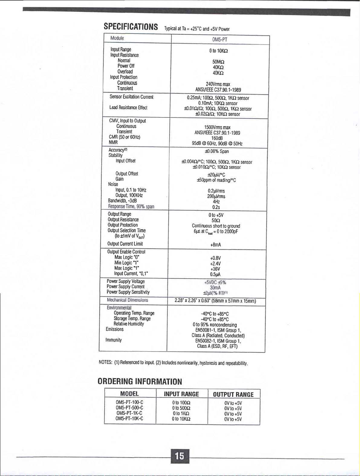
SPECIFICATIONS
hput
Range
Input
Resistance
Typical
Nomal
Power
Off
0wdoad
Input
Protection
Continuous
Transient
Sensor
Excitation
Gunent
Lead
Resistance
CMV. Input
Etlecl
to output
Continuous
Transient
(50
CMR
or
60flz)
NMR
AccuncYzr
Slability
Input
offset
0uput Offset
Gain
Noise
Input,0.1
Ouput,100KHz
Bandwidth,
to
-3dB
10Hz
0utput Range
OuFut
Resistance
Output Protection
OubutSeleclion
(to
0ugut
0uFut
Mu
Min
Max
Inpul
Power
Supply Voltage
Power
Supply Cunent
Power
Supply Sensitivity
tlmv of
Limit
Cunent
Control
Enable
Logic'0'
Logic'1'
Logic'1'
Cunent,
Time
VouT)
"0,1"
=
Ta
at
+25'C
ANS|/EEE
0.25mA
0.10mA:
r0.01CUA;
$.02Q/A;
ANS|/EEE
95dB
$.004CU"c;
$.010fU.C;
r5oppm
Continuous
6p
228' x226'x
power
and +5V
0 to 10Ko
50Mo
4oKO
4OKO
240Vrms
max
C37.90.1-1
1000,500Q,
1()K1Q
1000,5000,
15fi)Vrms
@ 60H2,
$.08%
100cl,5000,
at C*
0.60'
sensor
10KO sensor
max
C37.90.1-1
160d8
90dB @ 50Hz
Span
1OKO
€0PVfC
reading/.C
of
0.2pVrms
2O0pVrms
4Hz
0.2s
0 to +5V
50c2
shorl
to
g
=
1e 2g99pP
+8mA
+0.8V
+2.4V
+36V
0.5p4
(58mm
x
989
lKO
sensor
1l(f)
sensor
989
1Ko
sensor
sensor
ground
57mm x 15mm)
0perating Temp. Range
Stonge
Temp. Range
Relative
Emissions
lmmunity
NOTES:
Humidity
(1)Refuencedt0input
(2)lnc-tudesnontinearity,hysteresisandrepeaiability.
0 lo 95%
EN50081-1,
Clas A
EN50082-1,
ORDERING INFORMATION
MODEL
0M5-PT-1oGC
0M5-PT-5oG.C
0M5-PT-1K-C
0M5-PT-10K-C
INPUT
100o
0lo
0 to
5000
0to 1KA
0 t0101(ct
RANGE
-40oC
lo +85"C
-40'C
lo +85.C
noncondensing
ISM
(Radiated,
ISM
(ESD,
Class A
RF,
OUTPUT RANGE
Group 1,
Conducted)
Group 1,
EFI)
+5V
0V
lo
+5V
0V
to
0V
+5V
lo
+5V
0V to
Page 18

OMS.ITG
Thermocouple
FEATURES
O INTERFACES
THERMOCOUPLES
O HIGH
O 1500Vrms TRANSFORMER
O ANSYIEEE
O INPUT
o 160d8
O
95dB
o
10.05% AccuRAcY
O fl.OZIO
O
tlpV/'C DRlff
.
CSA CERTIFIED,
. MIX AND MATCH OMs TYPES
DESGRIPTION
Each OMS-ITC Thermocouple input
thermocouple
level
a high
switch controlled, allowing these modules
without the requirement
TO TYPES
LEVEL VOLIAGE
C37.90.1-1989 TRANSIENI
PROTECTED IO
cMR
NMR
AT
60H2. 90dB
LINEARfi
input which is filtered,
voltage
analog
J, K, T,
OUTPUTS
ISOLAT|ON
24OVAC
at 50Hz
FM APPROVED,
ON BACKPANEL
(Figure
output
of external multiplexers.
E, R,
S,
PROTECTION
CONTINUOUS
CE COMPLIANT
module
isolated,
1). This
to
C. N AND B
provides
amplified, and converted to
share a common analog
single
a
voltage output is logic-
channel
bus
Input
The
OMS-|TC can interface
J, K, T,
E, R, S, C, N,
a 0V to +5V range.
parasitic
for
terminals
provided
is
implemented
between
Signal filtering is
of normal-mode-relection
are
computer
After the initial field-side
proprietary
again using
mode
A special input circuit
of
power-line
screw terminals 1
on
the
spikes
Modules
Each module
thermocouples
the mounting
on
by
an internal
by installing
accomplished
field
side of the isolation
side.
chopper circuit. lsolation is
proprietary
a
or surges. The
voltages
up to 240VAC.
to nine industry
and B. tts
provides
conesponding
formed
backpanel.
pull-up
an external
and
3 on the
with
at
60Hz and 90dB
fillering,
lechnique
module is
protection
standard
is
cold-junction
by
the thermocouple
Upscale open
resistor.
to suppress transmission
Downscale
47Me
0M5-BP backpanels.
a six-pole filter which
at 50H2.
banier,
and
the input signal
provided
powered
against
thermocouple
output
signat
compensated
wire
thermocouple
indicatidn
resistor,
the
by
from +SVDC,
t20o/o
provides
poles
Two
other
four
is
chopped
translormer
accidental
connection
opeiates
tvoes:
bver
to
correct
and
screw
detect
can
be
tolerance,
95dB
of
this filter
are
on
the
by
a
coupling,
of common
r5%.
of
FIGUBE
1.)MS-|TC Block
Temp
Sensor
Diagram.
vcnrr
l/O
RD
Common
EN\
Page 19

S PE C I F I
CATI 0 N S Typicat
Module
Input
Range
lnput
Bias
Input
Input
CMV, Inpul
CMR
NMR
Accuncy
Nonlinearity
Stability
Noise
Bandwidth,
Response
0utput
0utput Resistance
0utput
Output Selection Time
0utput Cunent
Output Enable
Input
0pen
open
Cold
Power
Ponter
Power
Mechanical Dimensions
Environmental
Emissions
lmmunity
Curent
Raistance
Normal
Power
Otf
Overload
Protection
Continuous
Transient
to 0utput
Conlinuous
Tnnsient
(50H2
or 60Hz)
Input 0ffset
0utput
0ffset
Gain
lnput, 0.1
Output,
(lo
Mu
Min
Max
Cunent,
Input
Input
Junction
Acruracy,25'C
Accuncy,
Acruracy,
0penting Temp. Range
Stonge
Relati'ae Humidity
10Hz
to
100kHz
-3dB
Time,
90%
Range
Protection
Vor)
tlmV of
Limit
Conkol
Logic'0"
"1'
Logic
Logic'1"
"0', "1"
Raponse
Deteclion Time
Compenution
+5"C
to
-40oC
Supply Voltage
Supply
Current
Supply Sensitivity
Temp. Range
Span
+45"C
+85oC
to
T^ = +25.C
at
ANSr/rEEE
ANS|/EEE
95dB at 60H2,
See 0rdering Information
Continuous Shorl
6p
2.28' x2.26'x
EN50081-1, ISM
0 to 95% Noncondensing
EN50082-1, ISM
power.
+5v
and
0M5-tTC
{.1V to +0.5V
-25nA
50MO
4okc)
40kfi
240Vrms max
C3i.S.t-1989
1500vrms
10.02%
at C,*
max
C37.90.1-1989
160d8
90dB at 50Hz
Span
tlPV/'CG)
flltttfC
*25ppm/'C
02pVrms
2OOpVrms
4Hz
0.2s
0V
+5V
to
50c,
to Ground
=
0 to 2000pF
+8nrA
+0.8V
+2.4V
+36V
0.spA
Upscale
10s
$.250C
$.5.C
i1.250C
+SVDC
l5%
3OmA
t4Nf/"RTltti
(58mm
0.60'
-40'C
+&5.C
to
-40'C
+85"C
to
Group 1, Class
Group 1.
Class A
x
57mm x 15mm)
(Radiated,
A
Conducted)
(ESD,
RF,
EFI)
(1)
N0TES:
and
accuncy.
(3)Ihis
0.020'C/'C, Types ( T
Type
Type
Includes
repeatability.
(2)
is
equiralent
E 0.016"C/'C,
N
0.037.C/"C. Type
nonlinearity,
Does not
=
RTI
Relerenced
t0
Types R,
hysteresis
include
GJC
input.
to
.C
t0llou6:
as
0.025.C/.C,
S 0.168.C/.C.
C.0.072.C/.C.
Type
J
ORDERING
INFORMATION
MODEL
0M5-rTC-J-C
0M5-rTC-K-C
0M5-rTC-T-C
0M5-rTC-E-C
0M5-rTC-R-C
0M5-rTC-S-C
0M5-rTC-B-C
0M5-rTC-C1-C
0M5-ITC-NI-C
WPE
Type
Type
Type T
Type
Type R
Type
Type B
Type
C
Type N
J
K
E
S
-100'C
-100"c
-100"C
0'C to
0"C to
0'C
0'C
+350'C
-100'C
INPUT RANGE
to +760"C
+1350"c
to
to +400"C
+900oC
to +1 750'C
to
to
to
(-148"F
(-148.F
(-148'F
(+32"F
+1750'C
(+32'F
(+32"F
+1800'C
+1300'C
+1300'C
(+32"F
(+662'F
(-148'F
to +1400'F)
+2462.F)
to
+752'F)
to
+1652'F)
to
+3182'F)
to
+3182"F)
to
+3272'F)
lo
to +2372F)
+2372F)
to
OUTPUT
0V
to
0V
to
0V to
0V
to
0V
lo
0V to
0V to
0V
to
0V
to
RANGE
+5V
+5V
+5V
+5V
+5V
+5V
+5V
+5V
+5V
ACCURACY(I)
fl.07yo
fi.07Yo
10.09%
fr.07o/o
10.10%
fl.10o/o
fi.12o/o
fr.11o/o
fi.70o/o
10.61"C
10.97"C
10.46'C
10.59'C
!1.72"C
11.82'C
!2.21"C
t1.01"C
l0.98"C
Page 20

@"9ce
OMS.WBS
strain
FEATURES
O
INTERFACES
OR
OUARTER-BRIDGE
O
HIGH
o 1500Vrms
O ANS|/IEEE
O INPUT
O FULLY
o 100d8
O
IOKHz
+0.08%
o
+0.02o/o
a
+1pY/'C
O
O
CSA
CERTIFIED,
O MIX
AND
TO
LEVEL
VOLTAGE
TRANSFORMER
C37.90.1-1989
PROTECTED
ISOLATED
cMR
SIGNAL
BANDWIDTH
AccuRAcY
LINEAR|TY
DRlff
MATCH
Gage
lOOO
THRU
1OKO,
STRAIN
TO
EXCITATION
FM
APPROVED,
OMs
WPES
GAGES
OUTPUTS
|S0LAT|ON
TRANSIENI
24OVAC
SUPPLY
ON BACKPANEL
Input
FULL-BRIDGE,
PROTECTION
CONTINUOUS
CE
COMPLIANT
Modules,
HALF-BRIDGE,
wide
Bandwidth
DESGRIPTION
Baclganel
Term
Elock
input.circuits provide
fneclat.
isolated
excitation
supply
up
protection
to
240VAC.
of
the signal
3J
ft
v_-
2
inputs
uo-
uocornmon
RD
EN\
and
the
FIGURE
1.
jMS-WBS
Block Diaonn.
Page 21

SPECIFICATIONS
Typicat
T^ = +25oC
ar
power. FIGURE
and
+5v
2.
Full
Bridge
Gonnection.
Module
Range
Input
Inpul Bias
Cunent
lnput Resistance
Normal
Pouer
Otf
0wrload
Input
Signal
Proleclion
Conlinuous
Tnansiml
Effikn0$r(-1l-Z-g-5'c)
Excitation Output
Excitation Load
Excitation
Hall Eridge Volhge
Bridge Vothge
Hall
lsolated
Continuous
Tnnsipnl
Input
CMV,
(-4t,{l/&C}
Regulation
Stability
Level
Levd
Excitation Protedion
to
Outpul
Conlinuous
Tnnsient
(50
CMR
or
NMR {-3dB al 1OkHzl
60Hz)
Accunaryra
Nonlineadty
Stability
Input 0ffsel
0upulOtfsel
Gain
Noise
Input,0.1 to
Outout,
Bandwidth.
Rise Time, 10
Settino
0utput
Output
ouFut
10Hz
1@kHz
-3dB
to
90%
Time.
to 0.1%
Range
Resistarrcr
Protedion
span
Output Selection Time
(lo
fimv of VdJT)
outDut Currenl Limit
0uput hable
Ma<
Min Logic
Max
Input Curent,
Pounr Supply Voltage
Pouler $pply
Pouer Suooly
Medanical Dimensions
Environmental
Opding
Stotrg€
Relative
Emissions
lmmunity
Control
Logic'0'
'1'
Logic'1'
'0,1'
Current
Sensitivity
Tempenture Range
Tempenlure Range
Humidity
C3-C)
({}C)
Full Bridge
(x\|'$iBsts{}|
4,
tiqnv b
$.3nA
5oMO
40ko
40kct
240Vrms max
ANSt/tEEE C37.90.1
+10V l3mV
+3.3iIlV l2mV
$pprVml
t15ppny''C
240Vrms mu
ANq|TFFF n?7 0n r-roeo
1500vms max
NSr/rEEE
C37.90.r-1989
100d8
120d8 oer Decade above 10kH7
$.08%
Span t10pv Rno
$.02% Span
tlFVfC
*OpVfC
€Sopm
of
0.4pVrms
10mVo-o
10kHz
35ts
25016
l5V
50fl
Continuous
6t6 al
Shott to Ground
Cbod = 0
$rnA
+0,8V
+2.4Y
+36V
05lA
+5VDC
Full
170mA
228'
EN50082-1, ISM
Exc. Load,
QuVl% RTlt3,
x226' x
0 lo
EN5@81-1,ISM Group
Clas A
(58mm
0.60
-40"C
lo
-4tl"C
to
95% Noncondensing
(Radided,
Group 1, Clas A
-rrrB9lt2l-{/+c
t100mv
-1
C8e
NA
M
BeadinofC
to
2000pF
l5%
70mA
No
Exc. Load
x
57rnm x 15mm)
+85'C
+85'C
1,
Conduded)
(ESD,
RF, EFt)
Half Bridge
)liE tltsS38{B{.+liB93{
+5V tlmV
+1.667V
tlmV
2pVrms
\.'l
Rg{D
qu,
F9(t)
FIGURE4.
Rgot
Rg
"\
I
I
q&hSf?|Ld
'Sarp
NOTES:
hysleresis
Full
as
(1)Stnin
and repeatability.
A*b-aa
TffiAler
FIGURE
Bridge
3. HaIf
EGlg.Dl
Irilrlgld
-€rc|
!-lFl
ThH
modula.
element.
Bridge
0uarle
r Bridge
v
I
Slcct
(2)
|
Includes
(3)
Referenced
I
Gonnection.
Gonneclion.
excitation
error, nonlinearity,
to input.
ouswBs3aor-c
olttwBs.t€
oIs-ufBs€€
o||9UrBS{€
ou9wB95-C
ou9wBs3ll{3-c
oragwBs-ilc
oM-wBs384r€
oL$wB.s€-c
ilnnFt ltnklb
0Ms-wBs38{1-C
oMtwBg1-C
0Msrla$8-03-c
0M$w893-C
0Ms-wB$z-c
0M$WBS,I-C
oMtvvB$s.c
IIIPUT BRIIIGE TYPE IIIPIIT RIIGF
Full
Full
tlall
llalf
Full
Futl
Full
Bridge
Bridge
Bridge
Bridge
Bridge
Eridge
Bridge
l00Q
1*fi
lo
3{DO to 10ko
lmotolo(f)
300fi ro 10ko
300fi
10ko
to
1000to10ko
300cr
to 10kn
ErcraTlot OIITPI]r NAr|FF
3333V
3mV/V
at
10.0V
at 3mV / Sensitivity
3333V
a[ 3mV/Y Sensitivity
10.0V
d
3mV/V
l0.frv
d
2mv/v
3.333V
al 10nV/V SeNitMty
10.0V
10mV/V
at
Sensitivity
Sensilivity
Semitivity
Sensitivity
-5V
-5V
-5V
-5V
-5V
-5V
-5V
lo
to
to
lo
to
to
to
+5V
+5V
+5V
+5V
+5V
+5V
+5V
ORDERING
INFORMATION
Page 22

0M5-lul
FEATURES
O
ACCEPTS
O
UNIPOLAR
O
lSOOVrms
O
ANSI/IEEE
O
OUTPUT
a 110dB
o
400H2 SIGNAL
o
i0.05% AccuRAcY
O 10.02olo
O
CSA
O MIX
HIGH LEVEL
BIPOLAR
OR
TMNSFORMER
C37.90.1-1989
PROTECTED
cMR
BANDWIDTH
LINEARITY
CERTIFIED,
AND
FM
MATCH OMs
VOLTAGE
CURRENT
TRANSIENT
TO 24OVAC
APPROVED,
TYPES
OR PROCESS
OUTPUT
ISOLATION
CONTINUOUS
CE COMPLIANT
BACKPANEL
ON
Gurrent
CURRENT
PROTECTION
INPUT
0utput
Modules
DESCRIPTION
Each OMs-lVl
output. The
hold
mode where
and-hold
and conversion
Setting
module
is open
completely isolated
from Power
connection is required
proper
connect
A
special
against
lrack-and-hold
mode where
one DAC is
circuit,
of the tnct
piq
fS-.
hjOh,
or
Common,
operation
pin
23,
circuit in
accidental
currenl
output
module
circuit in
DAC
one
can supply
dedicated
each mod.ule
to a high
Wnqn
the hold
or
hold
level
mode is
pin
23 is tow,
mode is
computer
pin
16. This
between
the
ol
kack
the Write-Enable
the
to each module.
provides
current
controlted
the track
enabled.
side
circuit which
l/0
and hold
pin,
the output stage
connection
power-line
ol
provides
many
signal
output
single
a
input
stage can
output
modulei,
ln
addition
buffering, isolation,
(Figure
by
logic
the
inode is
The
module is
can
complete
Common
to
of the module
isolation
and
circuit.
For
l/0
Common,
voltages
power
a
provides
up
channel
of
analog
be operated
to
or
a track
the
track-
in
filtering,
1).
state
of WR
EN
enabted.
tf
pin
designed'with
be floated
to
means
that
r50V
Common
low
state,
simply
'lg.
pin
protection
to 240VAC
i
23
a
no
for
FIGURE 1.1MS4V|
Block Diagnn.
Backpanel
Term
Block
-<d
-<3
""
r,,c
lsolation
Earier
VrH / dw
UO Common
WR
EN\
/
-1,"
Page 23

SPECIFICATI0NS
Typicat
Module
Voltage
Input
Input
Input Voltage
Input
Range
Current Range
(-05)
Maximum
Current,
Muimum
(-05)
lnput Resistance
Input Resistance
0uput Current
Range
0ver
Ouput Compliance Voltage
(0pen
Resistance
Load
0utput I Under
ouput
Continuous
Transient
CMV, 0utput to
Continuous
Tnnsient
(50flz
CMR
(-3dB
NMR
Acflracy
Nonlinearity
Stability
Tero
Span
Noise
Ouput Ripple,
Bandwidth,
Rise Time 10ln !X)9[ Smn
(-05)
RanS
Capability
Circuit)
Range
Fzult, mu
Protection
Input
or 60Hz)
at 400
lkHz
-3dB
tlz)
bandwidth
Sample and Hold
Output Droop Rate
Acouisition
Track
Max Logic'0'
Min Logb'1'
Max Logic'1"
lnnrrl Crrrpnl
Porcr
Pou,er
Pnunr Srrnnlv Snnsilivitu
Mchanical
Environmental
Operating
Slonge
Relative Humidity
Emissions
lmmunity
'sarne
Time
an&Holrl
Enable Contol
'{l'
Supply Volhge
Supply
Cunent
Dimensions
Temp. Rang
Temp.
Bange
specitication
arT^ = +25oC
(0lo
40dB
2.28'x226'x
EN50081-1,
EN50082-1,
0
ISM Group 1,
powr
and +5v
Unipolar
Output
Cunent
0Ms{vl
l5V
or 0V
+5V
to
to
0
20mA
(no
ril6V
@map)
(no
75mA
damage)
5oMo
20a
0 to 20mA or 4
750fi
greder
240vrms max
ANS|/EEE C37.90 1-1989
1500vms
ANS|/EEE
oer Decade above 400H2
10.05%
10.02%
to 20mA
10%
2NDC
0
6500
t0
Powr
br
Supply
4.SVDC)
fm
26mA
max
C37.90.1-1989
10dB
1
Span
Span
Vdhge
d).5/v"c
f2oppnv"C
1OpApp
400H2
0 75ms
4()p{s
50c
+0.8V
+2.4Y
+36V
O 5rrA
+SVDC
l5%
170mA
J0SrrA/% lvn
(58mm
0.6'
+0'C
-400c
to
95%
ISM Group
x
57mm x 15mm)
+85"C
lo
+850c
t0
Noncondensing
(Radiated,
A
Clas
1,
Class
A
(ESD,
Condwied)
RF,
EFI)
ORDERING INFORMATION
MODEL
0M5-tvl-M-c
0Ms-rvr-A4-c
0Ms-tvt-BG,c
0Ms-tvr-Ao-c
INPUT
RANGE
0V
to
-5V
to
0V
to
-5V
to
+5V
+5V
+5V
+5V
OUTPUT flANGE
4mAto 20mA
4mAlo
OmA to 20mA
OmAto 20mA
20mA
BANDWIDTH
400H2
4001-lz
400H2
4ffiHz
Page 24

OM5-WMU/WU
Analog
FEATURES
O
ACCEPTS
O HIGH
1500Vrms
o
O ANSI/IEEE
O INPUT
100d8
o
o 10kHz
o 10.05%
O
fr.O2YO
O tlpV/"C
O
CSA
O
MIX AND
MILLIVOLT
LEVEL VOLTAGE
TMNSF0RMER
C37.90.1
PROTECTED
cMR
SIGNAL BANDWTDTH
AccuRAcY
LINEARITY
DRlff
CERTIFIED,
MATCH
uoltage
AND
VOLTAGE
OUTPUTS
IS0LAT|ON
-1
989 TRANSIENT
TO
24OVAC
FM
APPROVED,
OMs WPES
ON
LEVEL
SIGNALS
PROTECTION
CONTINUOUS
CE
COMPLIANI
BACKPANEL
Input
Modufes,
wide
DESCRIMON
A special
power-line
input
voltages
provides
circuit
up
protection
240VAC.
to
Bandwidth
against
accidental
connection
of
+E(C
9u*
-EXC
1. 0M1-WMV/W
+ln
-ln
Backpanel
Term
G
4
Y)
3
2
G
1
Block
Block Diagnn.
;i
Surge
Suppression
and
Protection
Anli-Aliasino
-J
I
Vour
l/0 Common
22
RD EN\
Page 25

S PEC I F|
Module
CATI
Inpul Bange
lnput Bias
Cunent
Input Resistance
Normal
Power
Otf
overload
Protection
Input
Continuous
Transient
Input
CMV,
Continuous
Tnnsienl
CMR
NMB
AccuracYtt
Nonlineadty
Stability
Input
Output
Gain
Noise
Input,0.1
Output,
Bandwidth.
Time,
Rise
Settling Time,
Output
Output Raistalre
0utput
0utput Seleclion
(to
Outout
0utput
Max
Min Logic'1"
Mu
Input
0utput
to
(50H2
60Hz)
or
(-3dB
10kHz)
at
Otlset
Oflset
1()Hz
to
100kHz
-3dB
10
to 90% Span
to 0.1%
Range
Protection
Time
tlmV
Vo,
of
Cunent Limil
Enable
Control
Logic T"
Logic'1'
Current,
Power Supply Voltage
Power
Supply
Power
Mechanical
Environmental
openaling
Stonge
Relative Humidity
Emissions
lmmunity
Curmt
Supply
Sensitivity
Dimensions 2.28' x2.26'x
Temp. Range
Temp. Range
0 N S rypinl
10.05% Span
)
'1'
"0',
EN50082-1, ISM
rt T^ = +25.6
*5v
rno
OM5-WMV
t10mv to tlmmv
r0.5nA
200Mo
4okfi
4okrl
240Vrms
ANSt/tEEE
ANSr/EEE
120d8
Continuous Short
6F al Ct"d = 0 to 2000pF
0 to 95% Noncudensing
EN50081-1, ISM
Clas A
C37.90.1-1989
1500Vrms
C37.90.1-1989
1
00dB
per
Decade above 10kHz
RTI{,)
t10pv
10.02%
Span
tlpV/'C
t4OpV/"C
f25ppm/'C
0.4pVrms
l0mVp-p
10kHz
35ts
250p
i5V
0V to
or
50c)
lf,mA
+0.8v
+2.4V
+36V
0.5llA
+SVDC l5%
3OmA
RTltzt
9pVl%
(58mm
0.60'
-40'C
lo +85'C
-40oC
lo +85'C
(Radiated,
1,
Group
Clas A
poner.
Max
max
$.05%(Vzc)
+5V
to Ground
x 57mm
x 15mm)
1,
Group
Conduded)
(ESD,
RF,
EFr)
OM5-WV
t1V
:0.05nA
650kQ
650kQ
650kCr
10.057o
span t02mV RTlt'?t
$.05% ru.o)
J201tV/"C
t50ppm/"C
2pVrms
i2DtlVlo/o RIIQI
l40V
t0
(minimum)
(minimum)
(minimum)
'
Same specification
WMV.
(1)
NOTES:
hysteresis
(2)
(3)
that rbulls in
Includes
and repeatabil
=
Referenced
RTI
is
V,
the input
voltage
0V outout
as 0M5nonlinearity,
ity.
input.
to
ORDERING
INFORMATION
MODB INPIITRANGE
0M5-WMV-1oA-C
0Ms-WMV-s0A-C
0M5-WMV-100A-C
0M5-WMV-108-C
0M5-WMV-508-C
oMswMV-1008-c
0M5-WV-1A-C
0M5-W-5A-C
0M5-W-10A-C
0M5-WV-18-C
0M5-W-58-C
0M5-W-108-C
0M5-W-20A-C
0M5-W-208-C
0M5-W-40A-C
0M5-W-4oB-C
-10mV
to
-50mV
to +50mV
-100mV
to +100mV
-1OmVto
-50mV
-100mVto
to
-lV
to +1V
-5V
to
-10V
to +10V
-1V
to
-SVto
-10V
to +10V
-20V
to +20V
-20V
to
-40Vto
-40Vto
+10mV
+50mV
+1fi)mV
+5V
+1V
+5V
+20V
+4OV
+4OV
+10mV
OUTPUTRANGE
-5V
to +5V
-5V
+5V
to
-5V
to +5V
+5V
0V to
+5V
0V to
to +5V
0V
-5V
+5V
to
-5V
to +5V
-5V
+5V
to
to +5V
0V
0V to +5V
+5V
0V to
-5V
to +5V
+5V
0V to
-5V
+5V
to
0V to +5V
Page 26

0M5-TX
FEATURES
o
IS0LATED
O
PROVIDES
TRANSMITTERS
O
HIGH
O lSOOVrms
O
ANSI/IEEE
O
INPUT
O IOOdB
O IOOHz
o
10.0570
a
fi.lzvo
O
CSA
O MIX
DESCRIPTION
Each
0M5-IX
nel which
standard
+20VDC
+20VDC
ISOLATION
LEVEL
TRANSFORMER
C37.90.1-1989
PROTECTED
CMR
SIGNAL
AccuRAcY
L|NEAR|W
CERTIFIED,
AND
MATCH
2-wire
rycepls.
+1
to +5V
regulated
CURRENI
VOLTAGE
TO
BANDWIDTH
FM
APPROVED,
OMs
transmitter interface
a 4
to
+2
or
power
2-Wire
L00p
SUppLy
FOR
NON-ISOLATED
0UTPUT:
24OVAC
ryPES
20 mA
to
supply is
+tV
to +5V
ISOLATION
TRANSIENT
PROTECTION
CONTINUOUS
CE
COMPLIANT
ON BACKPANEL
module
process
+10V
provided
cunent input
output
signal
to
Transmitter
2-WIRE
+2V
or
to +10V
provides
(Figure
powbr
a single
piovides
and
t1.
Rn
[ne cuirent
transmit-
chan-
a
isotateO
lnterfaoe
This
ter.
the
to
modute
supply
will
fh9.0M5-rx
field
transmifters.
between
room
computer.
The voltage
to share
multiplexers.
precision
A
sockets
resistor.
this
Alltield
voltages
voltages
liltering
side of
inputsarefu.lly
is
the isolation
allows
a
2-wire loop
without
provide
will
an isolated
output is logic
a
common
20f,r current
provided
are
Extra resistors
up
up
to
to
240VAC.
accomptished
requiring-an_extemar
a nominat
provide
lt can
also
2-wire
analog
conversion
on
the
protected
The
The
with
barrier,
Modules
powered
+20VDC
a 1500V
be
transmitter
switch
0M5-BP
are
available
module has a 3dB handwirtth nf 1nrir{z
module
a
and
transmitter
power
at a ldrop
isolation
used when
controlled,
bus without
from
has
six-pole
the
banier for
additionat
and
the input
lhe
resistor
is
backpanets
under
accidental
a
3dB
filter,
other
four
to be
direcily
suppty,
curenf
df
non-isorated
isotation
stage
which
allows
requiremenf
supplied with
io allow
part
number
connection
bandwidth
with
on the
of
potes
two
cbmputer
itie-regr]ibl
CmA
iJrequirei
of
tne cbniror
these
0f
the
instailation
oMX-1362-c.
power-tine
of
t0dHz.
on
connected
to?Omn"
2-wire
modules
;ne;n;l
module.
of
(innar
Signat
fieto
the
side.
2-Wire
Transminer
FIGURE 1.0M5-TX
Block
Backpanel
Term
Block
Diagnm.
20{2
0.1%
-<d
<3
plug-in
362€
""
r.,c
tr
vour
l/O
Common
RD
EN\
Page 27

S PEC
I Fl GATI
Module
Input
Range
Input
Resistor
Value
Acarncy
Stability
Loop
Supply Voltage
lsolated
Excitation
Continuous
Transient
Input
Protection
Continuous
Tnnsienl
CMV, Input
Conlinuous
Tnnsienl
(50
CMR
or 60Hz)
(+dB
NMR
Accunct'')
Nonlinearity
Stability
Input
0tfset
0utpul
Oftset
Gain
Noise
InpuL
0.1 to
0utput, 100KHz
Bandlvidth,
Response
Output Range
0utput
0utput Proteclion
0ulpul
0utput
0utput
Power
Povlet
Power
Mechanical
Envimnmenhl
Emisions
lmmuniiy
N0TES:
(2)
RTI
-3dB
Time, 90%
Raistance
Selection
(to
tlmv of
Curent
Enable Control
Max
logic
Min
Logic
Max
Logic
Input
Current,
Supply
Supply Current
Supply Sensitivity
Dimensions
0penting
Stonge Temp. Range
Relative
Humidity
(1)
Includes
=
Referenced
0 N S rvpior a Tr
Protection
to Oulpul
100H2)
at
1()Hz
span
lime
Vour)
Limit
"0'
"1"
"1"
'0,
1'
Voltage
lemp.
Range
nonlinearity,
input.
to
=
+25oC
Nominal
ANS|/EEE
ANSr/|EEE
ANSr/rEEE
120d8
10.05%
9:lpprnl"C
+1V
Continuous
6p at
180mA
at
100mA
x226'x
2.28'
0
EN50081-1,ISM
EN500B2-1,
hysleresis and
to 95%
Group 1,
ISM
rcpeatability.
power.
+5V
and
OMs-TX
4mA
to
20mA
20.00cl
10.1%
t10ppm/'C
20V
at 4mA
240vrms
max
C37.90.1-1989
240Vrms
max
C37.90.1-1989
1500Vrms
oer
:0.02%
+5V
to
+SVDC
lBosminer
lransminer
at
t10pV/% RTlo
0.60'
-400c
-4PC
Group 1
max
C37.90.1-1989
100dB
decade
above 100H2
span
t4FA
span
llpV/"C
n40pV/'C
of reading
l0nArms
50OpVrms
1@Hz
4mS
+2V
or
50c)
short lo
=
0 to 2000pF
Q*
+8mA
+0.8V
+2.4Y
+36V
0.5rtA
l5%
load
(58mm
+950c
lo
+85"C
to
noncon@nsing
Class
A(Radiated,
Ctas
,
to 20mA
RTlc)
+10V
to
gnd
of 20mA
bad of 4mA
x 57mm
x 15mm)
Cond$ted)
(ESD,
A
RF, EFI)
ORDERING INFORMATION
MODET
0Ms-rx-1-c
0Ms-TX-2-C
INPUTRANGE
4mA
20mA
to
4mAto
20mA
OUTPI'TRANGE
+1V
to +5V
+2V to +10V
Page 28

lE* -,4- . t
lllf-<-FM> ( ts
\,
>#
--
OM5-DT
General
FEATURES
INTERFACES
O
DEVICES
HIGH
O
o l500Vrms
O ANSI/IEEE
INPUT
O
FULLY
O
100d8
o
lKHz
o
o i0.10%
. fr.02%
O +2OpVl"C
O CSA
O MIX
SIGNAL
CERTIFIED,
AND MATCH
TO
REOUIRING
LEVEL VOLTAGE
TRANSF0RMER
C37.90.1-1989
PROTECTED
ISOLATED
cMR
BANDWIDTH
AccuRAcY
LINEARITY
DRIFI
Purpose
DC DISPLACEMENT
A
STABLE
OUTPUTS
ISOLAT|ON
TMNSIENT
TO
24OVAC
EXCITATION
FM
APPROVED,
OMs TYPES
TMNSDUCERS
DC
SUPPLY
PROTECTION
CONTINUOUS
SUPPLY
CE
COMPLIANT
ON
BACKPANEL
Input
AND
Modules,
OTHER
conkolled,
without
The
excitation
noise inherent
whict
the
requirement
0M5-DT
can interface
supply.
in
these
with
allows these
The lkHz
devices.
of
efiemal
to
devices
bandwidth
modules
Dc
Excitation
to
share
multiplexers.
which require
signiticdnily
a
comrnon
precision
a
reituces
analog
bus
10VDC
ripple
and
DESCR|
Each
tnnsducer
level analog
TION
0M5-DT
input which
voltage
genenl
purpose
is
output
Dc-LVDr
Transducer
input
fiftered,
isolated,
(Figure
1). This
+EXC
li
-ln
-EXC
Br
rcl9an€
Te
rm
provides
module
scaled, and
voltage
4
a
2
'l
Bloc
*-t
-€
4
b
5
3
a
single channel of
convefted to a high
is
output
Suppression
Protection
lu"
ruc
logic
Surge
anc,
+V
-V
switch
lsolated
Field€ide
Power
Special input
isolated
excitation
lsolated
Excitation
Source
circuits
provide
supply up
protection
to
240VAC.
-V
+V
lsolated
Computer-Side
Power
the
of
Power
Oscillator
signal inputs
20
19
22
17
16
and the
+5V
Power
Common
FIGURE 1.
0M5-DT Block
Diaoran.
Page 29

S PE Cl Fl
CATI
Module
Input
Range
Inpul Eias
cunent
Input Resislance
Nomd
Power
Ofl
Ovedoad
hput Protection
Continuous
Tnnsient
Excitation Voltage, V*.
Excitalion ornent
Excitalion Load Regulation
Excitation Stability
lsolated
Bcitation
Continuou
Tnnsient
lnput
CMV,
Continuous
Transient
(50
CMR
(-3dB
NMR
AocuncYtt
Nonlinearity
Stability
Input
Output
Gain
to Output
or 60Hz)
lkHz)
at
0tfset
Offsel
Protection
Noise
hput,0.1 h 10Hz
output, 100Ktlz
&ndwidth,
Response Time
0utput Range
0uhui
oulput
0utput Selection
Oulput
oulput Enable Control
Input Current,'0,
Power Supply Voltage
Power Supply Curent
Power Supply
Medanical
Environmental
Emissions
lmmunity
(1
Includes
)
(2)
BTI
-3dB
(to
90% final
Resistance
Protection
(to
Max
Min
Max
0penting Temp. Range
Stonge
Relative Humidity
=
Refermced
Time
Vour)
tlmv
of
Cunent
Limit
Logic'0'
Logic'1'
Logic'1'
1'
Sensitivity
Dimensions
Temp. Range
excitalion error, nonlinearity,
to input.
0 N
rvpir.r
S
value)
Tr = +25oc
rt
+5V
and
zMO
2[4O
2Mfi
ANSI/lEEE
C37.90.1-1989
+10.0V0C
40mA
240vms
ANSI/EEE
C37.90.1-1989
1500Vrms
ANSI/IEEE
200mA @ Full Exc. load,
228'x2.26'x
EN50081-1, ISM
EN50082-1, ISM
hysteresis
C37.90.1-1989
per
120d8
d).1% span,
il.02%
Continuous
6.016 at
+SVDC
900PVi%
0.60'
-40'C
-40'C
95%
0 to
Group
Group 1,
repeatability.
arul
power.
OM5-DT
rlv
to r10V
{).05nA
(minimum)
(minimum)
(minimum)
240Vms max
lS0ppsV'C
(formerty
f2mV
(maximum)
i5pprVmR
t1Sppm/.C
max
(formerly
mu
(formerly
lmdB
deca& above lkHz
RTlz
$2mV
span
f2OpVi"C
i40pV/'C
0.4pVms
5mVpp
llflz
750p
l5V
50f)
ground
shod to
=
C,-d
to 2000pF
0
rSmA
+0.8v
+2.4V
+36V
0.5FA
l5%
100mA @ No
Rflat
(58mm
x 57mm x 15mm)
+85'C
to
+85.C
lo
noncondensing
(Radiated,
1,
A
Class
A
Class
(ESD.
tEfE-472:)
lEfE-4721
IEEE-472)
Exc. Load
Conductd)
RF, EFI)
ORDERING
INFORMATION
MODEL
0Ms-DT-1-C
0M5-DT-2-C
0M5-DT-3-C
0M5-DT4-C
0Ms-DT-s-C
0M5-DT-&.C
0M5-DT-7-C
0M$.DT-8-C
0M5-DT-g-C
OM5.DT-1GC
MDflMUMINPUT
rlV
!2U
*3V
!4V
l5V
lsv
x7V
iBV
l9V
110v
0lmuT
l5V
l5V
l5V
15V
l5V
l5V
l5V
l5V
l5V
t5V
Page 30

@"€>(€
OMS.IFI
FEATURES
O
ACCEPTS
O
PROVIDES
O
NL
O 15OO
O ANSI/IEEE
. INPUT
o
10.050/o
O
MIX
O
CSA
FREOUENCY
HIGH
LEVEL
INPUTS
VOLT
TMNSFORMER
C37.90.1
PROTECTED
AccuRAcY
AND
MATCH
CERTIFIED,
INPUTS
LEVEL
VOLTAGE
ISOLATION
-1
989
TMNSIENT
TO
24OVAC
OMs
TYPES
FM
APPROVED,
Frequency
OF
O
to lOOkHz
OUTPUTS
PROTECTIO
CONTINUOUS
ON
BACKPANEL
CE COMPLIANT
N
lnput
Modufes
DESGRIMON
A 5.1v
excitation
closure
type
sensors.
excitation
common
is
arailable
The
excitation
pin
is
3
for
(+ln).
use
with
is
availabrd
on
pi'n
pick-up
magnetic
t
euil
or contact-
ano-
tir'e
Term
Block
-<d
-<4
""
""
A
special
circuit
accidental
connection
in
input
the
power-line
of
stage
of
the
module
voltages
ud
provides
protection
to ZqOVAC.
against
FIGURE 1.
1MS-lFl
Block
Diaoran.
Page 31

SPECIFIGATIONS
Inpul
Range
Input
Threshold
Minimum Inpul
Maximum Input
Minimum
Pulse
Low
Ofl
to 0utput
or 60Hz)
(0
to
Time
Vor)
of
"0'
"1"
"1"
"0,1"
Voltage
Range
nonlinearity,
to
0utput.
Width
g07d
00K-C
TTL Input
TTL
InputHigh
lnpul
Hysteresis
Zero
Crossing
TTL
Input
Resistance
Normal
Power
0verload
Input
Protection
Continuous
Tnnsient
Excitation
CMV, lnput
Continuous
Tnnsient
(50
CMR
AccunacY't
Nonlinearity
Stability
0ffset
Gain
Noise
0upulRipple
Response Time
0M5-tFFs00i1K-C
0MstFt-3K-c
0M5-rFt-5V10K-C
0M5-rFt-251V50tV1
0utput Range
0utput Resistance
0utput
Protection
Output
Selection
(to
tlmV
0utput
Cunent Limit
OuFut
Enable Control
Max
Logic
Min
Logic
Max
Logic
Input
Current,
Poiver
Supply
Power
Supply Curert
Power
Supply Sensitivity
Environmental
Openating Temp.
Stonge
Temp. Range
Belative
Emissions
lmmunity
N0TES:
(2)
RTO
Humidity
(1)
Includes
=
Referenced
Typicat
arTa
2.28'x2.26'
EN50081-1. ISM
EN50082-1,
hysteresis
and repeatability
=
+25C
+5V
and
0 to 100KHz
Zero
60mVp-p
350Vp-p
4gs
0.8V
2.4V
O.MV
1.5V
240vrms
ANSr/EEE
NSr/rEEE
Ca7.90.1-1989
+5.1V
@ 8mA
1500Vrms
C37.90.1-1989
120d8
{).05%
10.02% span
r40ppm/.C
140ppm/.C
<1OmVp-p
Input
@
300 ms
170
90 ms
20 ms
0V
to
Continuous
0 to
ISM
50c)
shorl
61s
=
C,*
at
+8mA
+0.8V
+2.4V
+36V
0.spA
+5V0C
110mA
r15q.V/% RTo
(58mm
x0.60'
-4fC
to
-40oC
to +85.C
nonconclensing
95%
1,
Group
Class A
Group 1,
power
Crossing
ma<
min
max
max
max
span
>2% span
ms
+5V
ground
to
Q 1s
2000pP
l5%
G)
x
57mm x 15mm)
+€5"C
(Radiated,
(ESD,
Class A
Conducted)
RF,
EFI)
ORDERING
INFORMATION
MODET
0M5-tFt-500-c
0Ms-rFt-lK-C
0M5-tFt-3K-C
0M5-tFl-5K-C
0M5-tFr-10K-C
0MslFt-25K-C
0M5-tFt-50K-C
0M5-rFt-100K-c
INPUTRANGE
0 to
500H2
0 to
lkHz
0
to
3kHz
0
to
SkHz
0
to 1OkHz
0
to
25kHz
0
to
50kHz
0
to 100kHz
OUTPUTRANGE
0V
+5V
to
+5V
0V
to
+5V
0V
to
+5V
0V
to
+5V
0V to
+5V
0V
to
0V
+5V
to
0Vio +5V
Page 32

@'@66
OM5-ITG
Linearized
FEATURES
O
INTERFACES
THERMOCOUPLES
O
LINEARIZES
O
HIGH
o
1500Vrms TMNSFORMER
O
ANS/IEEE C37.90.1-1989
O INPUT
o
160d8
o
95dB NMB
O
tlpv/"C DRIFI
O
CSA CERTIFIED, FM
O MIX AND
DESCRIPTION
Each
OMS-LTC thermocouple
thermocouple input which
conveiled
output is logic-switch
common analog
IO
ryPES
THERMOCOUPLE
LEVEL VOLTAGE
PROTECTED
cMR
AT
60H2,
MATCH
to a high level
bus
OUTPUTS
TO 24OVAC
90dB at 50Hz
APPROVED,
OMs TYPES
is filtered,
analog
controlled, allowing
without
J, K, T,
E, R,
S, N, AND
SIGNAL
|S0LAT|ON
TRANSIENT
input
voltage
the requirement
PROTECTION
CONTINUOUS
COMPLIANT
CE
ON
BACKPANEL
module
provides
isolated,
amplified, linearized
output
these modules to
of external multiplexers.
Thermocouple
B
a single
(Figure
1).
channel of
voltage
This
share a
Signal filtering
of normal-mode-rejection
are
the
on
computer
Afier
the initial
proprietary
again
using
mode
spikes
A
special input
power-line
and
is
field
side of
side.
field-side filtering,
chopper circuit. lsolation
proprietary
a
or
surges. The
circuit
voltages
Input
accomplished
the
provides
up
to 240VAC.
Modules
with
at 60Hz
and
isolation
technique
module
protection
a
six-pole
g0dB
at 50H2.
barrier,
and the
input
the
provided
is
to
suppress
powered
is
against
filter which
signal is
by transformer
tnnsmission
from
accidental
provides
poies
Two
other four
chopped
+SVDC,
connection
of
of common
l5%.
g5dB
this lilter
are
on the
by a
coupling,
of
FIGURE
1.
Temp
Sensor
AM}-LTC Block
Diagran.
+""
RD
EN\
Page 33

SPECIFICATI()NS =
Input
RanS
Inpul
Bias Cunent
Input
Resislance
Normal
Power
Ofl
0'/efload
Input
Protec{ion
Conlinu,ous
Transient
Accuracy
Stability
Input
0ffset
Output 0fiset
Gain
Noise
lnput,0.1
to 10Hz
outpul,
1OolGlz
Bandwidth,
Response
0utput Range
output
onrtput
oulput
0utout
output
Open Input
0pen Input
Cold
Power
Powt
Pounr
-3dB
TirE,
Resislance
Probction
Seleclion
(to
rlmV
of Vr,
Cunent
Linit
Enable Control
Max
Logic
Min
Max
Input
!'
Logic'1'
Logic 1'
Cunenl, !',
Response
Detedion
Junclion
Accuracy,
Acarrary,
Accurary,
Compensation
25'C
+SoC lo +45oC
-,|0oC
Supdy
Vollage
Supply Curenl
Supply
Sensitivity
90% Span
nmo
)
'1'
Time
b +&5'C
+25oC
and
+5V
l500vrm mx
NSI/IEEE C37,90. l-1 989
95dB
160d8
at 60H2,90dB ai SOHZ
See
Ordering
r1
PV/'Co)
*0ttVloC
r25ppry''C
0.2UVrms
3CJoUVp-p, 150pvnrE
4Hz
0.2s
Io +5V
0V
50()
Conlinuous Short to
6ps al
C-
=
+0.8V
+2.4V
+36V
0.5uA
Upscale
10s
r0.25oC
$.50c
tl.25oC
2.28'x2.26'x0.6'
Infornation
Ground
0 to
2000pF
ORDERING
INFORMATION
tlncludes
conformity,
hysteresrs aod
rep€alability
CJC
include
nol
0oes
accuracv.
Environrnenhl
Operatir€ Temp. Range
Storage
Relative
Emissions
lmmunity
MODEL
OMFLTC.Jl-C
OM5-LTCJ2-G
0Ms-LTCJ3-C
0Ms-LTC{4-C
oMtLTC-KI-C
0Ms-LTGre-C
OMFLTG-K3{
0M5-LTC-T14
0M5-LTC-T2-C
OM'LTGE-C
0Ms-LTC-R-C
0Ms-LTC-S-C
0M5-LTC-B-C
Range
Temp.
Humidity
TYPE
TypeJ
Type J
Type J
Type,t
Type K
Type K
Type K
TvpeT
T
Type
Type
E
Type
R
S
Type
Type B
0 to
-1,
ISM
Group 1.
EN50082n, FM Group I,
INPUT
lo +760oC
OoC
-100'C
to +300oC
lo +500oC
0'C
-100oc
OoC
0'C
-100oc
to
-100'C
OoC
ooc
lo +760oG
to +500'G
lo +200oG
lo +1000oc
(-148.F
lo +1(D0oC
(+32oF
+1350oc
+400'C
to
+500oC to +1 750oC
+500oC lo +1 750oC
+500oC
lo +1
800o C
-40"C
lo +85oC
-40"C
lo +85oC
95% Noncondensing
Class
Class A
(Radialed,
A
(ESD,
Condded)
RF,
EFI)
BAilGE OIIIPUT
(+32oF
+1400oF)
to
(-148oF
to +572oF)
(+32oF
to
lo
(+32"F
lo
to
(-148.F
lo +2462.R
(-148'F
to +752'F)
(+32'F
lo
(+32.F
to +1832.F)
(+9?'F
(+932'F
(+932'
F lo
932'F)
+1400oF)
+1&12'F)
+9?oF)
+392'F)
lo +31&2'F)
lo +3182'F)
+t272"
Fl
0V
lo +5V
0V lo +5V
0V
lo
0V to +5V
0Vlo +5V
0V
to +5V
0V
lo +5V
0Vlo +5V
0V
to +5V
0V
lo +5V
0V
lo +5V
0V
lo +5V
0V lo
(1)
NOTES:
Type
Type
Type
(Q
This
is equivalent to
J 0.020'CfC, Types
E 0.016"CfC, Types R, S 0
N
0.037'CfC,
Rderenced to inpul.
RAHGE
$.08%
+5V
+5V
r0.08%
t0.07Y"
t0.08%
t0 087o
$.08%
$.08%
$.16%
10.13%
t0.10%
10.10%
$.10%
10.1syo
"C
T 0.025'CfC,
K,
168"Cf
Type
072"CfC
C 0
ACCUMCYT
t0.610c
$.32'C
$.36.C
a0.70"C
$ 80"c
t0.38oC
x12oC
l0.80'c
t025'C
t1.0"C
t1.3oC
t1.3"C
t2.0'C
as lollows:
C,
Page 34

0ll,l5-AU
FEATURES
O
ACCEPTS HIGH
O PROVIDES HIGH
O 15OO
VOLT TRANSFORMER
o ANSilIEEE
.5
POtfS OF FILTERING
o 110d8
o 400H2
o
.
O MIX AND MATCH
O
cMR
SIGNAL BANDWIDTH
10.0570
fr.02% LINEARITY
CSA CERTIFIED, FM
AccuRAcY
LEVEL VOLTAGE
LEVEL VOLTAGE
C37.90.1 e-1 989 TMNSIENI
OMs
INPUTS
OUTPUTS
ISOITTION
TYPES
ON BACKPANEL
APPROVED,
CE COMPLIANT
Uoltage
TO
tlOV
TO
IlOV
PROTECTION
0utput
Modules
DESCRIPTION
eagn
p{.S-nV
output. Thetrack-and{rold
where
mode
whereone
circuit,
conversion
is required
of the
tnackand
Enable
The OMS-BP-MUX-C
control line,
output modules.
which
allows
voltage
output module
DAC
one
DAC is dedicated
each module
to a
between l/0
pin,
to
l/0 Common,
which allows
the track-and-hold
can
provides
high
level
Common
hold circuit.
backpanels allow
power
During
circuit in
supply nnny
to each modute. In
voltage
Fora low
pin
multiplexing
provides
the input
signal
output.
and Power
state,
19.
host computer
ot one
up, the
output remains
circuit
to be
a
single channel
stagecan
modules,
output
addition
buffering,
Common
simply connect
host
initialized.
tothetrack-and-hold
isolation, filtering,
lor
controt
DAC
0V
operated
be
or a kack
proper
pin
23,
of
up
to
to 64
output
of analog
in
a hold
mode
and
operation
th.e Write-
the WR
EN
0M5-AV
for
100ms,
FIGURE 1.
Bacleanel
Term Block
-<d
<€
0M5-AV Block Diaonn.
3ruc
6
""
*c
lsolation
Banier
Vr.r
YO
Common
WR
EN\
+5V
Power@mrnon
Page 35

S PEC
I Fl
CATIO
output
Volhge
0'ar Range
Oubut
0utput
Output
ouFut
Capability
Driw
Resistance
I Under Fault,
Protection
Transient
CMV,
0utputto
Conlinuous
Tnnsient
(50
CMR
or
60Hz)
(-3dB
NMR
AccuracYtt
Nonlinearity
Stability
Zero
Span
Noise
0utput Bipple, lkHz
at 400H2)
Range
Max
lnput
bandwidth
NS rypirrr
ar TAr
+25c and
+5v
r5V,
0
t36V
r5V,
0
5%
ANSI/EEE
ANSTnEEE
per
1ff)dB
$.05%
power
to +5V,
f10V,0
(no
damage)
50Mo
+5v,
to
t10v, 0
@ 10V
output
50mA
max
0.5c)
75rnA
C37.90.1-1989
1500vrms
d).02%
max
C37.90.1-1989
1 10dB
Decade
above 400H2
(&smA
span
span
+25ppm/"C
90ppm/"C
+10V
to
+10V
to
toad)
Sample
Acquisition
Tnack-and-Hold
Max
Min
Mu
Pouer
Power
Environmental
0perating Temp.
Stonge
Relative
RFI
Enisions
lmmunity
ORDERING
Hold
and
output
Susceptibility
(1)
Rate
Droop
nme
Enable
"0"
Logic
Logic'1"
Logic'1"
Voltage
Supply
Supply
Cunent
Range
Temp. Range
Humidity
Includes nonlinearity,
INFORMATION
MODET
0Ms-AV-1-C
0M$.AV-2-C
0M5-AV-$C
0M5-AV-4-C
0Ms-AV-$C
0M$AV-6-C
0M5-AV-7-C
Control
EN5008_1-1,
hysteresis
INPI'TRANGE
0V
-5V
-5V
0v
-10V
-10v
-5V
350mA Full load.
228'
x2.26'x
0 to
d).5% Span
lSM.qroup
EN50082-1, ISM
and
repeahbility.
to +5V
lo +5V
to +5V
+10v
to
+10V
to
to +10v
t0 +5v
+0.8V
+2.4V
+36V
0.5uA
+5VDC
l5%
135mA
No load
0.60'(58mm
-40oC
-40.C
95% noncondensing
enor
Group
lo +85oC
to +85'C
at 400Mflz,
1,
Class
A
1
Ctass
,
x 57mm
x
SW,
3ft
(Radiated,
Conducted)
(ESD,
A
RF.
OUTPUTMNGE
-5Vlo
+5V
-5Vlo
+5V
0V
+5V
to
10V
+10V
to
10V
+10V
to
+10V
0V
to
10V
+10V
to
EFn
'
Page 36

0M5
The
following
mount
mounting
mechanical
the 0M5 modules.
pins.
drawing is
Many
As
an example,
Module
useful
if designing
sockets
are available which
AMP
provides
Inc.
[22@'nu
Dimensions
circuit
a socket with
2255'(57.3m)
(57.4mm)l
boards to
accept
the
part
and
number
50865-5. The
obtainedlrom PEM
Pinouts
(Penn
KFS2-M3.
g1s"!'-o:Tl-j
captive
nut lor
Engineering
the
3mm mounting
and Manufacturing),
screw
part
can
be
number
-ln
-EXC
-SEN
0.900'(22.9m)
,?
-:22
o
o
t'16
6
5o
o
o
o
o
oz
1
Top View
1.175'(29.8m)
RD
EM
vour
Vr
PowerCommon
+ln
+EXC
+SEN
l,lOTES:
RD
EN\
Vow
VN
PowerCommon
+ln
+EXC
+SEN
(t)
A| dmslrsims
(2)
Mo$ting
Bonom
pin ptating
^^23
o
o
o
o
o
o
te17
r'\
6
o5
o
o
o
2o
1
View
ara Typtcal-
is
ZoF
-ln
-€xc
-SEN
untes oth€Mis€ not6d.
in. gotd.
Page 37

Accessories
FEATURES
O
SINGLE,
O
DIN
O 1g-INCH
O
MULTIPLilED
fSD' <FM>
\5
DESCRIPTION
DUAL,
8-,
AND
RAIL
MOUNI
MOUNTING
BACKPANELS
MCK
AND
NON-MULTIPLEXED
>rgg5-BP-10-G
Interdannet
Bridge
Jumpe6
for
1o-POSITION
FOR
BACKPANELS
BACKPANELS
BACKPANELS
p0slil0l{
10
0M5
Analog
AllAt0G
Modules
O INTERFACE
MODULE
O
. CABLE-TO-SCREW-TERMINAL
l/0
Figure
2
terminals
for
connection
SPEGIFICATIONS
Openting Tempenature:
Interhce
Field
"
Looic
17.4'(44aomm)
CABLES
EVALUATION
BOARD
INTERFACE
BAGKPANEL,
for
schematic).
at each
to
Connedor:
Field
module
site.
the host
system.
il0N-MUlflptExED
connections
use
system
--40"C
to +85.C
95% retative
High
Density
2Fpin,
male header
are
interface
humidity,
Screlv
BOARD
terminated
norrcondensing
Clamp,
connector
with
cable
0Ms-cA-04-01
t4
AWG
four
N4ax
screw
FIG
U R
26
Conductor
Conneciors Pl,
Suraged
Thru
Hole
1.
Conneclor
Mating
Connectors
E 1.
0M5-BP-1
pin
Male
P2(r)
3.05'
w
-"
Ph
Standoff
0.15'(3.8mm)
b
Connector
Pl and P2
6-C
Pin
Pitr2
Channel
Dia
Berg
65863{75 or
is Amp 49958€
Anat og l/0
1
+5VDC
equivatent
are wired
Backpanel
SLpply
or equiralent.
paralel
in
D inensions.
tor.daisy
Socksts
chaining"
'\
up to
lor Curcnt
4
boards.
Conversion
Besisiors,
OMX-1962€
'rs
0.14'(3.6frun)
inside
diametet
0.o8'
16
(e.ornrirl
(32.4mm)
10.32
Grourd
LW,
NlJt
ard Lockwasher
Cold
Junelion
Compensdrbn
X
0.40
lncluding
Ciraril
Page 38

z.
ll,
o
E>>
F
62
o
x
UJ
+
+
I
to
IX
IT
(o
@
o
x
ut
+
c
+
o
T
o
)<
UJ
I
FO
@@
cc
CC
@o
oo
o
Fs
cf
a
o
h6
9o
EA
tr5 oi
5
a
E?
IE
E
-
olt
t!
E
EEEEEEsEEEEEEEEEEAESE6
FIGURE
2. 0M5-8P16-C
Dlo
Eor
o!
('E
-J
Fg
.0D(9
A'E
E
E
6
Schenatic.
Page 39

ELECTRICAL
P1
AND P2
Connection
connectors
both
input
ADJACENT
Adjacent channels
signal
isolation.
through J P1
BP-16-C
Example:
position
lf
JPl is installed,theoutputof
2, which
CONNECTOR
to
the host
are
electrically
analog input
and
output
and analog
connectors.
CHANNEL
may
from
an
isolated
This
capability
5
headers
on
schematic
Assume
and
an OMS-lVl
provides
two
system is made
equivalent.
output
JUMPERS
be
connected together to
input module,
provided
is
El
and E3. A simplif ied
E2,
,
for
Channel 1 through 4 is
an 0M5-|MV input module is
module is installed
output
Channel
levels
1500V isolation.
of
at connectors
Two
connectors
from host
providing
with the 15
P1 and P2.
provided
are
systems having
provide
isolated
an
two levels
iumpers
drawing
shown
installed
labeled
of
in Figure
in
in Channel 2
1 isconnectedtothe
inputof
These
to allow
individual
output
1500V
of
JP1
the 0M5-
3.
Channel
1
position.
Channel
GROUNDING
a
dehils
fOure
0M5-BP-16-C
Jumper J3 connects
lf the host
ground potential.
C
proper
For
the optional
backpanel.
the SENSE tine
system has
opention
using the 0M5 backpanels,
power
logic
can
exists
ground
common
be established
elsewhere
loops
on the 0M5-BP-16-C
in
the system,
could exist.
ground
Jumpers
the
capability, this
of
the output switch
a cunent
and module l/0
jumperJ4
0ther
jumper
configuration
J'|,
J3,
and J4
(pin
25)
to the backpanet
altows
measuring
or track-and-hold
path
must
exist
Common (module
jumper
via
should.6e
connections
power
of
available
are factory
instailed.
signat
the OMS-BP-16-
circuit when
between
removed
the host
pin
1g).
J4. lf
this connection
Since
ground
OMs
Module
and
on
the
ground.
control
path
This
possible
signal
FIG
URE 3. 0 M5-BP-|
POWER
The 0M5-BP-16-C
mounted
chassis
power
any combination
FUSING
The
0M5-BP-16-C
Littlefuse
protection
voltage
fuse
type
by
connection is
will
F1
backpanel
0M5-PBT-003
backpanel
252ffi4, 4
clamping
be blown.
6-C Adjacent Channel Junpen.
requires
of modules.
power
amp fuse. Zener
the input
reversed,
this
extemal
power
supplies
is fuse
power
voltage
zener diode will
+5VDC
have
protected
diode
+5.6V.
to
be
pwer.
,5%
adequate capacity
through
F1. This
provides
DZ1
lf the
forward biased
input
The
to
is a
extna
supply
and
FIGURE
ground
system.
lf
measurement
the backpanel
ohms;1@
the SENSE line
Forlull
0M5 modules,a*10-3?
electrical connection
provided
connection is made,
shield wires and
input
system,
modules
4.
0M5-BP-16-C
usually occur
the connection of
system,
signal
is
ohms
to R., when
protection
modules and
J1
against
with
a large
backpanel
should
are used or if
Grounding Diagnn.
at the A/D
power
common
an optional
ground
can
recommended
a
lhis
large
ground
between
a
a ditferential input is
be removed.
this
gauge
wire
possible
signal
the host
vocoM 19 16
D/A
or
conveder
AGND
and
resistive
made via
be
value.
ground
configuration
electrical disturbances
is
stud
ground
stud
of
shortest
the
ground
loop
ground.
Remember
system does not
of the host measurement
shield wires
connection
R,.
JumperJ2
provided
and system
could
lf
the
used
that J1 is required if
between AGND
R, can be as
can be used to connect
is used.
on
on the
possible
result
application involves only
by
the host measurement
have differential inputs.
PWFCOM
exists in the host
and
large
as 1 0K
thefield-side ofthe
backpanel.
ground
length. When
through the
An
be
should
this
AGND
output
Page 40

@@
0M''BP'10-MUX'G
p'stTt'tf
10
Ar{At'G
r/0
BAGK'A*EI,
MUtTrptExED
DESCRIPTION
tempetature
compensation
schematic).
each
eacn
daisy-chained.
0M5-CA-04-01
26
Pin
sensor
Fierd
module
modute
site.
site.
Conductor
Connector
Mate
is
mounted
for
thermocouple
connectioni-are
Up
to four
use
orr,tx-cRg-O1-C
cabte
for
conhecting
pt(r)
I.backpanel
rixture.
re
0MS-Bp{6-MUX-C
nd
one
the
q,
"ilTn*#lil"lJ'lilT
input
modules
ierminateo
0M5_Bp_16_MUX_C
cabte
to
host
(Figure
S)
lt
can
mounted
be
for
analog
output.
switch
contr6lbd'outputi
Figure
lSed
wiin
iour
screw
Oacfpanefimiy
iiiiliiil,
Jriaining
computer.
can
$',$'j,llh'il
6 for
accept
any
on
the
has
two
This
two_
on
tie
-
--
-
terminars
at
Ue
and
17.q
SPECIFICATIONS
Address
Input
Logic
Lewls:
"0,
Looic
Logic'1'
'1"
"0'or
EN
Signal
Pl
to
Channel3
(address
Detav
G15)
I
S63)
1{6
l, Inpul
RD
EM or lilR
trom
@42.Otffiri
Max
Min
Cunent,
Conneclor
Standalone (address
Expanded
High.Density&rav
4o-ptn,
mate
0.1UA
1.0$
51ns
64ns at
100ns
'l26ns
neader
ma\
at
-25.C
max
at 25.C
-25.C
at
25.C
-25"C
at
Ctamp,
clnneclor
25.C
to +gSoC
to +85oC
-T-
i4
AWG
to +85"C
0.15'
(3.8mm)
r.275.
Max
Swaged
Thru
Hole
1.
Connector
Mating
FIGURE
5.
Pin2
Pin
ReadAddress
Selection
Standoff
(3.8mm)
0.15.
Connector
0M5-Bp-16-M|JX-C
1
Junper
ls
Berg
+SVDb
Chann€l
Dia.
6586&075
is Amp
Suootv
''
or equival€nt
4995g-6
Anatog
'w'ite
'
Selec{ion
I
o,
equivalenl
t/0
Backpanet.
Address
Jumper
Conversion
Resistors,
OMX-t
g6Z-C
0.14'(3.6mm)
inside
diameter
Ground
Nut
Cold
Compensation
I
2.27'
(57.7mm)
I
I l-1z.cmm1
:-T-
1o.75'(19.1mm)
Fr I
'
L-!
10.32
X o.zto
Lug,
and
Lockwasher
Junclion
o.oss'
lncluding
Circuit
Page 41

z
IIJ F
o
cc>>
o
z
z
lll F
o
E>>
63
6=
=
o
o
0-
o
X
ut
+
cF
+o
c
=€
IE
o
@
q
o
6
=
o
o
o
X
U
I
c
o
g
=
o
o
.L
o
)<
lt
s
o
G
T
()
c)
o-
o
o
=
+
o
()
o
x
rlj
Z;
ai
ci
-
@
9q
E-
E
-
dF
fo
I
F
-af
EE
E
o
o
i99;99;9
dl
l<
FININ
ototo
o
6S
6E
GO
(b
.E,
g)E
o a) <
i99;9s;9
l< rco
FININ
(9l(,l(9
().D
l(,
I
<
g;9
!99y99;9
t< r(o
FININ
OIOIO
cD6|FO
dt
<
lo
o<
a
z
O
gt
9a
zz
<
i99i9g;9
l< rd!
6lSlE
o .o
(o
b
ts
lo
F
<
FIGURE
6.
1Mi-BP-\
6-M
UX-C
Schematic.
EFggEFu'EPEES;sst*EF
5
EE
Page 42

ELECTRIGAL
Pl
CONNECTOR
GROUNDING
Figule
7
below
the
0M5-Bp-1
details
6-MUX-c
installed.
the
optional
ground jumper
backpanEt.
conf
.lurirpers
.ri,
iguration
Ji,
il};
avairabre
on
;;dr;
ADDRESS
El Jumper
4
?
SELECTION
Pos
2
1
0
To
connect
conf
iguration,
POWER
The
power.
adequate
FUSING
multiple
OMs-Bp-l6-MUX-0
use
interconnect
0M5-BP-16-MUX-C
The
chassis
capacity
mounted
to
E2
Jumper
pos
4
J
2
I
I
0
cable 0Ms-CAB-01
backpanel
0MS-PRT-003 power
power
any combination
Address
O-15.
48-63,
32-47,
16-31,
Range/lVlode
STANDALONE
EXPANDED
EXPANDED
EXPANDED
O-15, EXPANDED
backpanels
in
-C.
requires
external
of modules.
this
expanded
+SVDC
supplies
r5o/o
have
J-umper
J2
ff.the.host
MUX-C
connects
sysrem
ground
the
sNS
has
rhe
capabirity,
potentiat.
(pin
L0 rine
rhis
4)
to
the
artrws
meiiuring
backpaner
signar
thiolG-iiF-jo-
ground.
FIGURE
7.
J2
Rl
0M5-Bp-16-M|X-C
Grounding
Powar
r/ocoM
Common
Signal
Grounct
and
Grounding
Diagnn.
Eolt
OMs
19
Modub
16
PWR
COM
Page 43

@
90Ms'BP'sHt'c
F2'801{E
/Tw0
posrTr0ir
AnAt0G
r/0
BAGKpAt{Er.s
DESCRIPTION
The
OMS-BP-sKT-O
modules.
modules.
see
Tie
-2-C
The
They
g
Figures
and
following.acces-sories
panel
(Figure
Qlv
a
I
2
The
followin_g
SKI-
Oty
2
2
({Panets1-Z
(4
The following
accessories
-2-C
panets:
or
(# panets))-4
x
DIN
is
0M5-Bp-2-.c
both
are
DIN
10
for
wiring
8):
rair
styres
a singre
are required
Model
OM7-DIN-SF
0M7-DIN-SE
are required
Modet
OMZ-DIN-SF
OMZ-D|N-SE
OM7-D|N-WSF
OMZ-D|N-CP
channer
is
a ouat
rail
comoatible.
diagrams,
mounting paner
channer
Figures
for mounting
Description
Base
Sideetement
for
mounting
Description
Base
Side
Baseetementwithoutsnapfoot
Connection
are
available.
!N !0022-35x7.5
EN
50035-G32
EN
50022-35x15
specify
(strified
mountin!
paner
i
1
and 12
one
0M5-Bp-sKf-
element
two
or
etement
etement
pins
length
in
(stoned
steet)
steet)
(slofted
steel)
for
the
for
the
for
schematics.
with
snap
more
0Ms-Bp-
with
snap
foot
meters (-XX)
0M5
OMS
foot
SPECIFIGATIONS
0pemting
TemDerature:
Interface
Connectoc
Field
Logic
or
-40'C
to +85"C
95% relative
High
High
humidity,
Density
Screw
Density
Screw
L_
OM7-DIN.WSF
mounls
non-condensing
Ctamp,
t4
Clamp,
EN 50O22-35x7.5
EN 5O022-3Sx1S
EN
50035€32
AWG
14
AWG
to
DIN
rails
_
-
oM7-DtN.SF
OM7-DIN.CP
Mu
Max
OM7-DIN-SE
Sal@ts
tor
I
I
F
bE
-E
I
I
Sodcts ,il
OMXGJCC
Gonp€nsadon
Curst
Co|wst-
Cr€il
CotdJwtioo
Chdjf
n""Sto.,
Coil€Fion
Fesislq,
OUX-tg62C
ooof,o
OMX-i
362.c
O
f,o%oo"
PNor
Commn
+5V
l/O
@tr{/-.li
Vin/U
Vb/tvwldn
PwsCm
+5V
l/O@liy-tn
/+lr CH
CH
FIGURE
A
B
8.
DIN
Rait
FIGURE
Mounting
9.
Elenents.
0M5-B10A-C
Wiring
Diagnn.
FIGURE
10.
0M5-8P04-C
Wiring
Diagran.
Page 44

PCOM
+5V
vo
cot /
-{61
v,J
v^,-,
+:tJ'
FIGURE
1
l.
-EXC
-l,V
+trV
{rrt +Od
1MS-BP-SKT-C
+EXC
Schematic.
,o
COti/V
dw
unt"H
-lN
-lN
CHACHB
0MX-1
not
installed
362-C
at tactory.
resistors
are
FIGURE
1
2. 0M5-BP-2-C
Schenatic.
Page 45

@'€>oilrb-BP-g.
C
8 POSITIO]I
AI{ATOG
BACKPA]IEL,
YtI
]IOII.MUTTIPLEXED
DESCRIPTION
9t':!0it(
0M5-BP-l6-c
permits
providing
Jumpers
7)
0.15'(3€mm)
jumpers
connecting
two levets
on the
(i.e.
or
high
Swaged
S-landoff
Thru
Hole
(6)
permit
equivarent.
an input
of isolation (Figures
0M5-Bp-8-c
channels
8{5)
Tolerance:
paralteling
An
additioirar
module's
permit
user
two
set
output
addresses.
tO.O20' (tO.SOmm)
26
Conductor
Mde
Conneclors
OMS-Bp-8-C
inter-channer
of
to
an
if,
il;.
serection
Pl'l
Pl,
P2(t)
boards
output mooire;i
(i.e.
of row
I
E
E
@
o
o
€
ts
N
n
o
o
o
Pin2
Pin
1
P:tn2
Pin
I
to form
a
bilogijurperi
iriput,
channers
NOTES:
+sVDC
(l)
0-
5.8.
(147.3mm)
SuppV
Connector
MatlrE
Connectors
Daisy
A lemperature
compensation
sensor
is mounted
forthermocouple
SPEClFICATIONS
0penting
Tempenture:
Interface
Connector:
Field
Logic
10.0'
(254.omm)
9.7'
(246.3mm)
9.5.
Soc*ets lor
C,onversion
b
Berg 65863{75
connector
pl
and
Chainingf
up
Cunent
Ftesislors,
b AMp 49959€
p2
arg wired
to I
boards.
OMX-I
or
362-C
equivatent.
or equivalenl.
parallel
in
input
-40"C
95%
High
2Fpin,
tor
on
each
modutes
+85.C
to
relative
humidity,
Density
Scrav
male
header
channel
to
(see
Fijure
0onrondensing
Clamp,
conneclor
(3.8mm)
Compensation
Field
YO Termination. (B)
provide
1 4 for
14
AWG
Max
0.15'
10.32
Ground
Lug,
Nul
and
Lod$asher
oMx-cjc-c
Cold
Junction
Analog
Signat
junction
cold
sctiemaiii-
E
N
@
F
N
x
0.40
lnctudlng
Circuit
FIGURE
13.
1Mj-BP-A-C
ELECTRICAL
ADDRESS
SELECTION
Anatog
t/0
Backpanet.
ADJACENT
l,lllf[{rlryls
srgnar
iso.lalion.
CHANNEL
rom
an isotated
This
capabitity
JP7.
JUMPERS
may
beconnected.
input
module, providing
provided
is
together
with
ihe
to
sevei
provide
an isolated
two levels
lumpers
outpur
0f
15d0v
tabeted
Jp1-
Page 46

@.
a o
I
o @ Fo
999999
4lql4l4lqlqlq
)<
IJJ
ia
'c
CG
r6
o-
o
o
o
o
.LN
IN
o
B
Pro
-o
(5E
P9
-oo
g)E
=
o
6
o
)<
UJ
I
Z-
si
d
FNO
ooo
c66
o()o
EEEEEE;;;;;;;EEEEEEEFE
cgccccccca
-EE-E.E.E-EFEFFEEE"
6665665S68586
FIGURE
|
4. 1MS-BP-B-C
Schenatic.
Page 47

@'9
0Ms-BP-B-MUx-c
poslTl0il
I
A*AL0G
r/0
BAGK'ANEL,
MurilplExE'
DESCRIPTION
Jumpers
channels
0.15'(3.8mm)
Swaged
Standott
Thru
Hole
(6)
on
the
0M5-BP-g-MUX-C
0-7)
Dia
(i.e.
or high
(19.lmm)
3.r5'
(80zriln)
0.75'
225.
(572mm)
permit
26
Conductor
Ph
g-1
lO.O20'
channels
Tolerance:
Male
user
selection
5) addresses.
I
E
E
F
E
ul
d
N
@
F
ts
b
o
o
o
Read
Address
Seleclion
Jumper
Write
Selection
of tow
Address
Jumger
+5VDC
(i.e.
5.8'
(147.3mm)
Supply
NOTES:
SPECIFICATIONS
Openating
Tempenture:
Interhce
Connecton
Fietd
Logic
Address
Input
Logic
Lerals:
Logic
Logic'1'
'0'or
EM
Sockets
Resistors,
Berg
65869{Z5
b AMp
"0'
"l'
Signat
Detay
to
Channels
(address
(address
8-63)
for
CuBent
OMX-I
o,
49959€
I, lnput
RD
from
(t
Connector
)
MatirE
Mu
Min
Curent,
EM
or WR
Connector P1
Standalone
Expanded
10.0'
(254.0mm)
9.7'
(246.3mm)
9.5'
(241.3mm)
Conve6io.t
b
connector
0-7
tr7)
362-C
equivalenl
or
eguiyalent.
-40"C
95%
relalive
High
Density
2$pin,
0.8v
2.0v
0.1pA
1.0pA
51ns
64ns
100ns
126ns
to +85.C
humidity,
Screw
male
header
max
max
at
25.C
-25oC
at
at
25.C
-25.C
at
non+ondensing
Clamp,
14 AWG
connector
at
25.C
-25.C
+85"C
to
+85"C
lo
to +85.C
0.15'
(3.8mm)
10.32
Ground
Nut
and
oMX-CJC€
Cold
Junclion
Comp€nsation
Banier
Strips
Field
Analog
UO
Termination.
Mu
E
N
a
o
ts
N
X
0.40
Lug,
Inctuding
Loc*washer
Circuit
for
Signal
(g)
FIGURE
15.
0MS-BP-A-M|X-C
ELECTRICAL
ADDRESS
SELECTION
lnatog
t/O
Aackpanet.
backpanel.
modules,
output
address
Address
The
and
modules.
range.
Selection
Read
Address
1!.q9ttnt
1
2
3
4
5
Read
Address
the write
The
table
Jumpers
lUrite
Jumpe{Ht)
group
below
shows
Address
6
7
8
9
10
group
Address
assigns
a
set
assigns
the
colrelation
AddrG
Banse
0-15
Stand
4&63
32_42
tuianded
1F31
Exianded
0-15
ExdandeO
of 1
6
addresses
a
set
of ro
ot
atone
Expanded
for input
aooresseiioi
poiitidnio
iumper
Page 48

z.
UJF
o
E>>
z.
lll
E
C)
z
B=
F
t8r=
o
o
><
uJ
5a
i6
s2()
uJ.
tl
o
C)
g
o-
o
6
+
o
o
@
6
F
o
X
ut
+F
+o
+c
T6
!ro
UJ
I
I
atE
Q>9r
gs5
O==
Has
nO
-c
>tt
oc
o6
F6
Arp
6E
=
o
ql
SsE
o
o
s
F
z
r.lj
o
=o
.IP
E
t4t
+
fl-*..)$to
(9NFO
lo
EEEftET
@
G'
F99r9gi9
-
rt
6l$18
t\
sT
_v
dt<
., ,.
z.
IIJ
3
<
f<oxoo
g;9
I
l('
d)<
ggggEg
i99i9g;9
l< rco
FININ
(9t(5to
6()
C)
z
61
?l
Nt
ol
NI
NI
()
to
<
FIGURE
1
6.
0Mi-BP-]-MUX-C
Schenatic.
Page 49

@
I
oMb-Bp-l6-DIN-0,
DESCRIPTION
These
are the 0M5-BP
ing
option.
anodized
aluminum,
These
I
or 16
backpanels
which
channel
are
attached
in turn
backpanets
to
a 0.062"
is captured
using
0Mb-Bp-l6-Mux-Bllrl-Gn
OM5.BP-8.MUX.DIN.G
with a DIN
the 0M7-DIN-SF
piece
thick
rail
of
mount-
black
and
0M7-D|N-SE
DIN rail
assembled.
mounting
elements.
0Mb-Bp-g-DlN.G,
These backpanels
come fully
DESGRIPTION
The
0MX-1363-C
and
the
0M7-lF
3.480'(88.39mm)
3.378"
3.103' (78.82mm)
is
a 19-inch
interface
3.62'(91.gsmm)
3.12" (79.2smm)
0.062' (1
(85.8omm)
0.378" (9.6omm)
o.tos" (z.ozmm)
board
57mm)
o'=i
(16.oomm)
-_-l
-1
-
-
l
OMX-1363-C
metal
rack
for
mounting
17
for
0.31'(7.87mm)
(34.93mm)
1 .375'
O
O- 0.141'(3.58mm)
O
O
r
o.6s'
(See
Figure
-
-
[i-
- O.125'(3.17mm)
oo
O
@
19
the 0M5-BP
dimensions).
2 PL
2 PL
@@@
@@.
O
PEM
INCH
Dia
o\o
3mm metric\
nutT
PL
METAT
backpanels.
pL
I
lt
also
MOUNTING
provides
o@
capability
17.60'
(447.04mm)
o.2
(5.46mm)
RACK
to mount
t 5'
II
0
0Ms-pRT-003
the
1.10'
(27.94mm)
2.60"
(66.04mm)
power
suppties,
-
3.00'
(76.2mm)
-
0-50'
(12
7mm)
FIGURE
| 7.
0MX-|363-C
DESGRIPTION
The
0M7-lF
is
a universal
of
the
0MX-1363-C
FIGURE
|
8.
0M7-lF
mounting
Anatog
interface
board which
rack or
universal
lnteiace
Rack
Dinensions.
OM7-iIF
UNIVERSAT
converts
on a DIN
rail.
Required
Board
Dimensions.
a 26-pin
mounting
INTERFAGE
ribbon
cable input
hardware is included.
to 26 screw
BOARD
terminals for
Use 0M5-CA-04-01
r-/i.t!<'Oc,a
discrete
wire.
cable
lt can be
(See
Figure
mounted
1 8 for
on the
dimensions).
back
Page 50

OM5.BP.SKT.G
DESCRIPTION
The
OMS-BP-sKT-C
module,evaluation
connectionsare
junction
couple
The
using
Two
path
(module
common
switch
sy:temr
exist.
at
Jumper
the
tion
terminals.
compensation,
sockets
to
compensation
temperature
modules. (See
0MS-BP-sKT-0
the
following
2
0MZ-DIN-SF
2
0MZ-DtN-SE
4
0M7-DlN-Cp
jumpers
a'e
between
pin.19).
and
module
or track-and-hold
jumper
Other
connections
the A/D
or
D/A
J2 is
used
compensation
voltage
to
correct
lf
an
J2
labled
cJC+and
an
ambient
temperature
circuit
is
(Figure
connected
sensor
Figure
is
elements:
provided
power
+5V
path
A
u0
J1
should
converter
in
the
circuit
for
external
should
is VcJc
a singre
mechanically
channer
9)
Al
]
to
terminalblocks'foreasb
circuit
20 for
board
with
signar
input/output,
is
included
schematic).
compatibre
base
elements
side
etements
with
snao foot
connection pins
for
customer
Common
must
common
circuit.
be removed
power
of
of the
junction
cold
is
enabred
the
thermoelectric
simulation
be removed.
cJC.-.An
+25
of
=
0.5.|0
use. The
(module
exist
between
proper
for
lf
this
connection
since
ground
host
measurern'ent
f irst,
pin
the host'controirogic
operation
possible
and
signar
compensation
wirt
provide
and
bffect
voltage
is
desired
The
externalvoltage
externalvoltage
The
"c.
traniJer
-{.0025(T-25)V.
AiIALOG
a test
socket
for
contror,
and
oluseraciess.
for
evaruation
with
J1
,
16)
of tne
exists
ground
giouno
system.
circuit.
proper
rne
at the
+ln'and
of
st o."o
function
of
DrN rair
provides
dnO
mounting
a
Common
fO
mooure
elsewhere
toopi
usuaity
lf it
is installed,
compensa-
-rri
tor
jtncti;;
coid
is
applii,o
rv
iortesponoi
or ttre
oriooail
MODUTE
0M5
powei
AioN
thermo-
Resryed
4.25.
cunent
power
riutpui
in
lne
coufi
occui
screw
artne
(1oEm)
FIGURE
19.
EUATUATIOII
A
g7
Contol
RD
EM
WR
EM
PCOM
+5V
PCOM
@
trfl
l'l
la\l
lvl
TB3
BOARD
o^
o"
o
a)
Lr-r--+
::j-J l_-:r
)Ms-BP-sKr-c
Evaluation
Board
L@al UO
n2
l---] '.
-'
|
|
o*
-Ott
tl
U
J2
Dinensions
And
A
(J,
@
vo
vo
pin
Lavout.
coM
coM
FIGUBE
20
NOTES:
1.
Jl
and J2
2.
SCMXCJC
3.
ResistorSCMXRl
resistor
0
M5-BP-SKT-C
RD
EM
WR
EN\
Reserved
PCOM
are factory
is
a CJC
tor
cufient inputs,
Eval
uation
installed.
temperature
is
an optional
not faclory
Board
Schenatic
sensor.
W
conveGion
installed
J1
I
/777
PCOM
Page 51

0M5-GA-04-01,
DESCRIPTION
0l[x-cAB-013-G
IIITERFIGE
GABltS
0M5-CA-04-01
system
BP-8-C/0M5-BP-B-MUX-0
cable
(figure
FIGURE
interface
with
cabre
a mass-terminated
211.
Colored
Cable
OD
DO
DD
DC
otr
OD
DD
oa
DD
DD
o!
DD
Dfl
2t.
0M5-CA-04-01
Stripe
is
Assembled
for
the
backpaners.
on
System
0M5-CAB-01-C
0M5-Bpr16-c/0M5-Bp-16-Mux-c/0M5-
This
is
a rm
26
socket
to
tnbrtace
connector
instated
Cabte
conductor
tril
DD
trl t-l
DD
OD
CE
Dtr
trO
DD
L'
rln
Dtr
Dtl
on
each
Socket
Conneclor
t-l
ribbon
Pin
Daisy-chain
0M5-BP-16-MUX-C
end.
Connector
1
FIGURE
cable
Colored
Cable
is
Pin
1
Socket
22.
of
Pin
trD
oo
DO
OD
trD
D!
C!
DD
oo
trD
DO
trD
trD
0MX-CAB-01-C
provides
and
eight
Stripe
on
Assembled
Conneclors
1
interconnection
between
0M5-Bp-8-Mux-c
to
Pin
I
oo
oo
oo
oo
oo
oo
oo
oo
oo
oo
oo
oo
Connector
_____-j
feet)
Cabte
Pin
1 Merer(3.3
Daisy-Chain
a
maximum
backpaners
Cable
(Figure
n r-1
DD
trl r-l
OD
DD
oo
trD
oo
OD
DD
!D
trD
DD
of
four
22)-
Socket
Connector
Pin
1
FIGURE
23. Apptication
OMX-CAB{
TO
HOST
SYSTEM
0f
oMX-CAB-o1-c
1-C
r/)
oM5-CA-04-01
0MX-CAB-01_C
Daisv_Chain
OI\
IX-CAB
I
1€-
,--^- -
Cabte
I
n
il
il
oMs-Bp€
oMs-Bp-B
oMs-Bp-B
oMs-Bp-B
Up to
or 16-MUX-C
or 16-MUX-C
or I6-MUXC
or 16-MUX-c
I
I
I
eight
OMS-Bp-8-MUX-C
backpanets
Page 52

@'
I
0 lttlx'GJ
DESGRIPTION
SPECIFICATIONS
G-G
EI{GApsuLATED
cotD
J
ulr
GTf
0N
G0
pEtsATr
M
oil
Accuracy
+25"C
+5oC
to
-40'C
DESCRIPTION
Package
the
output
16-MUX-C
jumpers
10
of
of
any input
backpanet.
for
module
@.@
DESCRIPTION
precision.20O.
A
input
module
locrgtp-a1g
One
pr9'vided
0MX-1362-C
Qf
or
0M5-rX
is
y",
10ppm/o0
two-wire
on
ar backpanets
shipped
:O.ZS.C
+45oC
to +85'C
|
I
I
fO.s.C
tt.zS.C
0MX.1344
connecling.
OMX1362.C
wiih
adjacent
lo
input
the
resistor
tnnsmitter
each
of
used
interface
ro
ailow
module.
inpuvoutput
an ddiacenioutput
GURRENT
with
the
mooub
instattation
FIGURE
JUMPERS
modules
on
the
0M5-BP-l6-c
module.'inJirmpers
GONVERSIOII
0M5_llcurrent
zsi.
fioure
otltiis"'el'irtoi.
n
-E(C
-SEN
24. 1MX-CJC-C
backpanel.
can
also
physiat
This
bb used
lor
RESISTOR
D.
+SEN
Dinensions
connection
configuring
is
l/0
pin
And
made
addresses
if
it is
Layout.
desired
on
to direct
the
0M5-Bp_
FIGURE
25.
0MX-1362-C
Physiat
Dinensions.
0.05'(t.3nm)
(t0.2mm)
o..as.
Ph
winh =
o.04o.
(r.o2mm)
Page 53

ollf
5-pnT-000,
0M
5-pnr-003-220
p0wtn
$upplf
t$
DESCRIPTION
The
0M5-PRT-003
220UAC
input.
combination
mounting
capabitity
They
of
0M5
Linear
have
sufficient
modulgq.
for
the
p-ower
Supplies
ouput
trre
0M5_pBT_00S
are
availabte
cuuenicipacrtv
ol,rx-iioc-ciletar-racr<
power
iufpties.
in
120VAC
b
Jpiiffy
piriirri
or
SPECIFICATIONS
Module
Input
Voltage
47Hzto63Hz
0utputVoltage
0!4ut
output
0perating
Dielectic
(input
Line
(1
0% line
Load
(50%
0uFd
overvoltage
(taciory
Both
suppries
Recognized (Fire
Range,
Current
(at
Cunent (at
Temp
Withstand
grouno
to
Begulation
change)
Regulation
load
change)
(rnax)
Rippte
protection
set)
are
tested
Number
+70"C)
+So.C)
Voltage
and
E55974)
certified
and
by-TUV
to
csA
certirieo
0M5-PRT-003
104-132VAC
+
SVDC
l
7o
3A
bA
0 to
+70"C
37sovAc
+0.057o
t0.05%
5mVp-p
*0.4V
6.2V
vDE
0806
and
nle
lcsn
0M5-PRT-003-220
207-265VAC
5V0C
0
to
3750VAC
*0.05%
+0.057o
5mVp-p
6.2V
rEc
380. They
'-uiruer
r-nseazgl.
*1%
3A
64
+70"C
+Q.4Y
are
uL
l-lo
I
I
AC Power
Llne
Conneclor
ru"e
5.90'
(149.9mm)
I
@
o
|
4.87
(123.7mm)
|
|
,o-o-
This
slde
mounts
to
SCMXRK-OO2
_o--o_
@
o
flGUnE
26.
1MS-1RT-1IJ
physicat
Dimensions
Page 54

|S
/D
re
:
cA,s
warranty
n
CLA|
free
g^fj:fS-qL"
WARRANTy
coverage
to
on
M
E
in
aoos
cover
each
:,:N,::
R
materials
handling
product.
;;;,.11.
a
n-
ado
::,;*gs1:;;::
and
workmanship
ition"
and
i
shipping
:., |
:11,7,:-
;,;
."
J'
ii'i' il.".r,
iirn".
.
:,t,,,
for
fhi"
a
.;!:E|.;:-i;::;;:'?'t;i:i:.:::.::.:.:'j.::.|.'';:.:;:'':::RETURNREoUEsTs/|NoU|RlEs',z;.?
rests/inquiries
O
OMEGA,
S
CUSTOMER
ned
AR
purchaser
The
breakage
FO.R
WAR.RANTY
following
contacting
1.
Purchase
was
PURCHASED.
2.
Model
warranty,
3.
Repair
relative
i#:Si."#:',l,iii""S#:"'"'^?T,:U:ilt"R,H:fr?:er
OMEGA
@
copyright
is
and
a
is responsible
in
transit.
serial
product.
the
oMEGA
RETURNS,
number
number
trademark
information
OMEGA:
Order
and
instructions
to
registered
2oos
for
shipping
ptease
avaitable
and/or
ENGINEEBING,
BEFbiE
under
of
the
specific
- -"--
'
of
OMEGA
which
have
the
product
the
product
problems
F''
iwClruegntruG,
lNc.
Arr
i?i,llfl,ii,?i;'Jilll",liliU^iEtXg.Anlf#;.;i.
to
the
PURCHASER
number
charges,
under
rights
;ilii#ll'l??nine-readabre
oMEGA.customer
SERVICE
shourd
freight,
ron
Tor
}4-U9I
DEPARi[i'ii,Ji'iIN
then
insurance
|:oN:tUABFANIY
current
information
1.
Purchase
of
the
repair,
Model
Repair
relative
chanses,
tNC.
reserved.
and
instructions
to
whenever
T_!is
OBiAiN;'i"NUTHONIZED
be
markeJ
and proper
repair
charges.
available
Order
do,cyle1t
number
serial
product.
the
an
improvement
roi-,-il,
service
on
ih"
REPAIRS,
Have
eEronE
to
number
and/or
may
not
*noru
Department.
ORDER
ort"id"
packaging
TO
of
consutt
the
following
;"il;;;;
cover
the
COST
of
product,
the
specific
is
be
probfems
possibre.
copied,
o,
in part.
rhis
photocopied.
without
BEFoRE
RETURN
AVOID
the
return
prevent
to
oMEGA
oMEGA:
and
arrords
the
Page 55

omega.eom"
Canada:
U.S.A.
Mexico:
OMEGAnet@
omega.com
For
immediote
and
Canada:
Online
Service
Servicing
One
Omega
Stamford,
TEL:
FAX:
e-mail:
976
Laval (Quebec)
TEL: (51a)
FAX:(51a)
e-mail:
CT
(203)
3s9-1660
(203)
359-77W
info@omega.com
Bergar
856-6928
856-6886
info@omega.ca
technicql
Sales
Service
Customer
Engineering
En
Espaflol:
e-mail:
(001
FAX:
info@omega.com.mx
:
Service:
Service:
(001)
espanol@omega.com
203-359-7
)
p.O.
Drive,
06907
HZL
-800-826-63
1
-800-622-297g
1
203-359-2803
North
-0047
5A1,
or
7-800-872-9436
807
Americo:
Box
4047
Canada
opplicotion
-
42
7
}00-TC_OMEGA@
/
/
Internet
e-mail
info@omega.com
ossistqnce3
1.-SO0_622_BESTo
/1_800_USA_WHEN@
Czech
Republic:
Germany/Austria:
United
ISO
It is
regulations
Approach
The
gl'oJs
wARNING:
Kingdom:
9oo'l
Certified
policy
the
information
!t
of
that
Directives.
contains,
These
oMEGA
applv.
contained
and
products
Frystatska
TEL:
FAX:
Toll
e-mail:
Daimlerstras
TEL
F
Toll Free
e-mail:
One
Northbank,
M44
TEL:
FAX:
Toll Free
e-mail:
Engineering,
o.y!9A
oMEGA
in
this
reserves
are
not
Servicing
784,739
+420 (0)59
(0)59
+420
Free:
0800-1-66342
info@omegashop.cz
se
26,
(0)7056
+49
AX: +49 (0)7056
in
Germany:
info@omega.de
Omega
sBD
+44 (0)167
is
will
document
the right
deJignea
Drive,
Irlam,
United
777
(0i)r67
+44
in
sales@omega.co.uk
coistantly
add
United
lnc.
ttre
to
"rt"i
roruse
777
to
ie'mart
is
believed
ip""iti""tion.
01
Karvind,
6311899
6311114
-7
D
5-392
9398-0
9g9B-29
0800
River
Bend
Manchester
Kingdom
66tI
6622
Kingdom:
compry
prr"ring
in,
and
with
to-every
to
be
should
Europe:
Czech
Deckenpfronn,
639
767g
Technology
0g00-4gg_4gg
ail
worrdwide
"il;;ili;
but
not
b" ,i"J
J
oMEGA
""rtiii""ii."
correct,
*iil,ori;;t";.-'
Republic
'
Germany
Centre
safety
il"proor"t.
device
accepts
for,
human
and
EMc/EMl
to the
upon
European
certification.
no
liability
applications.
for
New
any
Ml516
t1208
 Loading...