

Page 1
TM
User’s Guide
Shop online
at
omega.com
e-mail: [email protected]
For latest product
manuals:
www.omega.com/en-
us/pdf-manuals
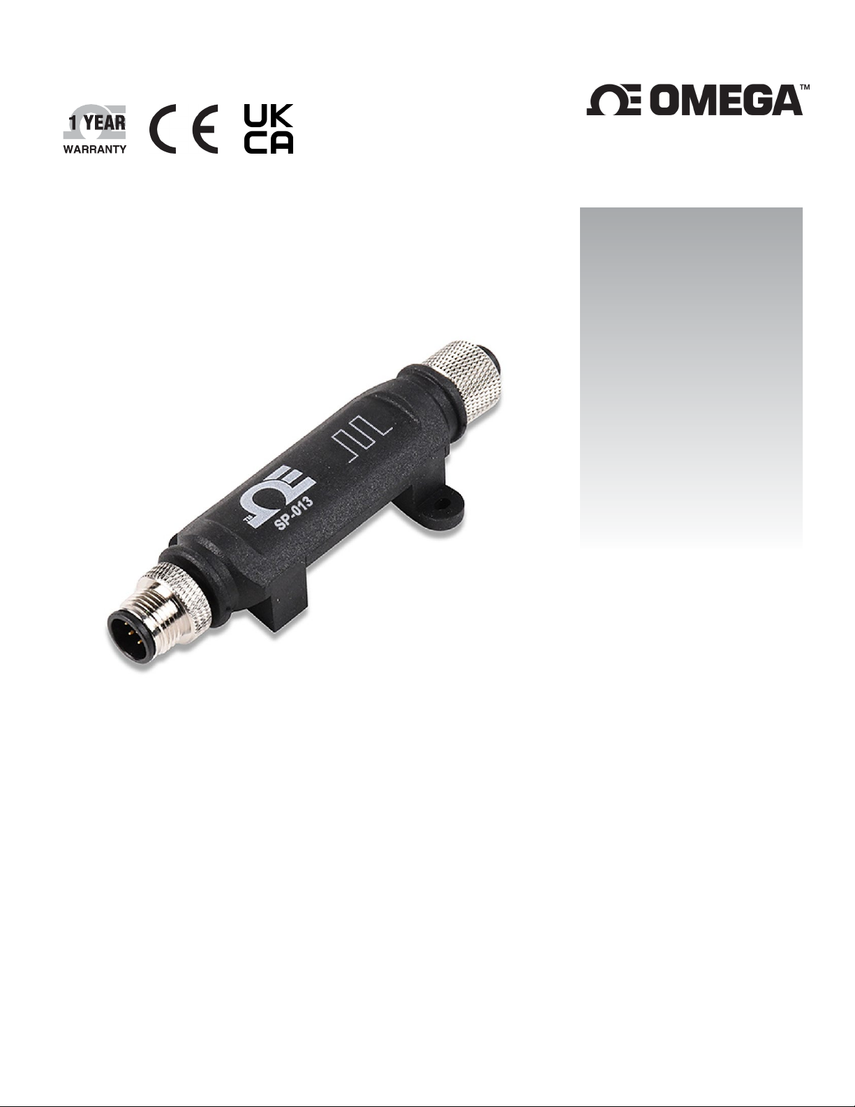
SP-013
Layer N Digital Pulse Smart Probe
Page 2

The information contained in this document is believed to be correct, but OMEGA accepts no liability for any errors it contains and reserves
the right to alter specifications without notice.
omega.com [email protected]
Omega Engineering, Inc:
Tel: (203) 359-1660
e-mail: [email protected]
Fax: (203) 359-7700
800 Connecticut Ave. Suite 5N01, Norwalk, CT 06854, USA
Toll-Free: 1-800-826-6342 (USA & Canada only)
Customer Service: 1-800-622-2378 (USA & Canada only)
Engineering Service: 1-800-872-9436 (USA & Canada only)
Omega Engineering,
Limited:
1 Omega Drive, Northbank,
Irlam Manchester M44 5BD
United Kingdom
Omega Engineering,
GmbH:
Daimlerstrasse 26 75392
Deckenpfronn Germany
2 | M5751
Page 3

Table of Contents
1 Notes, Warnings, and Cautions .................................................................................................................... 5
2 Introduction ................................................................................................................................................. 6
3 Specifications ............................................................................................................................................... 7
4 Hardware Setup ........................................................................................................................................... 8
4.1 Connecting to your Layer N Smart Interface ...................................................................................................... 8
4.2 Digital Input Wiring Diagram ............................................................................................................................ 8
4.3 Discrete I/O ..................................................................................................................................................... 8
5 SYNC Configuration ...................................................................................................................................... 9
5.1 Connecting to SYNC - Automatic Detect ............................................................................................................ 9
5.2 Connecting to SYNC – Manual ........................................................................................................................... 9
5.2.1 Communication Interface.................................................................................................................................... 9
5.3 Input Configuration .........................................................................................................................................11
5.3.1 Digital Inputs Interface ...................................................................................................................................... 11
5.3.1.1 Pulse Measurements ................................................................................................................................................... 12
5.3.2 Mixed Input Interface........................................................................................................................................ 16
5.3.2.1 Digital Inputs (Mixed Mode) ........................................................................................................................................ 17
5.3.2.2 Process Inputs (Mixed Mode) ...................................................................................................................................... 17
5.3.3 Discrete Input/Output (DIO) ............................................................................................................................. 18
5.3.3.1 Setting DIO as an Input................................................................................................................................................ 19
5.3.4 Advanced Scaling Options ................................................................................................................................. 19
5.4 Output Configuration ......................................................................................................................................21
5.4.1 Device Output Range/Types .............................................................................................................................. 22
5.4.1.1 ON/OFF Output Type .................................................................................................................................................. 22
5.4.1.2 Pulse-Width Modulation (PWM) Output Type ............................................................................................................. 22
5.4.1.3 SERVO Output Type .................................................................................................................................................... 22
5.4.2 Sensor Output Mapping .................................................................................................................................... 23
5.4.3 ON/OFF Control Module ................................................................................................................................... 24
5.4.4 Setting an Alarm ................................................................................................................................................ 25
6 Pairing a Sensing Device to a Layer N Gateway .......................................................................................... 26
6.1 Wireless Pairing ..............................................................................................................................................26
6.2 Wired Pairing ..................................................................................................................................................26
7 Appendix: SP-013 Registers ........................................................................................................................ 27
7.1 Digital Descriptor ............................................................................................................................................27
7.1.1 Digital Descriptor .............................................................................................................................................. 27
7.1.1.1 Digital Measurement Types......................................................................................................................................... 28
7.1.1.2 Digital Data Type/Format ............................................................................................................................................ 28
7.1.1.3 Digital Configuration ................................................................................................................................................... 28
7.1.2 Digital Input Device Byte ................................................................................................................................... 29
7.1.3 Digital Sensor Parameters ................................................................................................................................. 29
7.1.3.1 IPSO Digital Definition ................................................................................................................................................. 30
7.1.3.2 Digital Resolution ........................................................................................................................................................ 30
7.1.3.3 Sensor Trigger Function .............................................................................................................................................. 30
7.2 Process Input ..................................................................................................................................................30
7.2.1 Process Descriptor ............................................................................................................................................ 30
7.2.1.1 Process Measurement Types....................................................................................................................................... 31
7.2.1.2 Process Input Data Type/Format ................................................................................................................................. 31
7.2.1.3 Process Input Configuration ........................................................................................................................................ 31
7.2.2 Process Device Byte .......................................................................................................................................... 32
3 | M5751
Page 4

7.2.3 Process Sensor Parameters ............................................................................................................................... 32
7.2.4 Process IPSO Definition ..................................................................................................................................... 32
7.2.4.1 Process Resolution ...................................................................................................................................................... 32
7.2.4.2 Process Sensor Trigger Function .................................................................................................................................. 32
7.3 DIO Interface ..................................................................................................................................................33
7.3.1 DIO Descriptor ................................................................................................................................................... 33
7.3.1.1 DIO Sensor Type .......................................................................................................................................................... 33
7.3.1.2 DIO Data Type/Format ................................................................................................................................................ 33
7.3.1.3 DIO Input Configuration .............................................................................................................................................. 33
7.3.1.4 DIO Device Configuration ............................................................................................................................................ 34
7.3.1.5 DIO IPSO Definition ..................................................................................................................................................... 34
7.3.1.6 Sensor Trigger Function .............................................................................................................................................. 34
7.4 Output Interface .............................................................................................................................................35
7.4.1 Scaling Minimum / Maximum Values ................................................................................................................ 35
7.4.2 Output Values ................................................................................................................................................... 36
7.4.3 Output Names ................................................................................................................................................... 36
7.5 Digital Output Configuration ...........................................................................................................................37
7.5.1 Rate ................................................................................................................................................................... 37
7.5.1.1 PWM Rate ................................................................................................................................................................... 37
7.5.1.2 SERVO Rate ................................................................................................................................................................. 38
7.5.2 Output Type ...................................................................................................................................................... 38
7.5.3 Active State ....................................................................................................................................................... 38
7.5.4 Mapping Enabled .............................................................................................................................................. 38
7.5.5 Sensor Mapping ................................................................................................................................................ 38
4 | M5751
Page 5
1 Notes, Warnings, and Cautions
If the equipment is used in a manner not specified in this manual, the protection by the equipment may be impaired.
Do not operate the equipment in flammable or explosive environments.
It is important to read and follow all precautions and instructions in this manual before operating or commissioning
this device as it contains important information relating to safety and EMC. Failure to follow all the safety
precautions may result in injury and/or damage to the equipment.
The following labels identify information that is especially important to note:
Note: Provides information that is important to successfully set up and use the SP-013.
Caution or Warning: Informs about the risk of electrical shock.
Caution, Warning, or Important: Informs of circumstances that can affect the functionality of the instrument and
must refer to accompanying documents.
5 | M5751
Page 6
2 Introduction
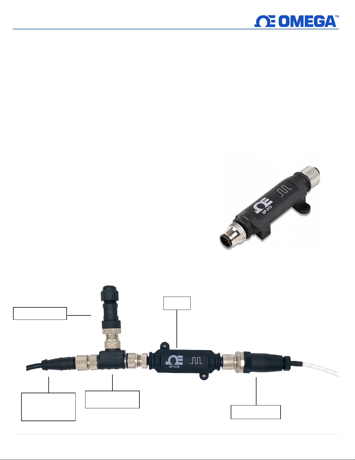
IF-001
Interface
SP-013
M12.5-S-M-FM
Figure 2: Example SP-013 integrated into a Layer N ecosystem
M12.8-S-M-FM
Figure 1: SP-013 unit
M12.8-S-M-FM and
M12.8-T-SPLIT
The Layer N SP-013 Digital Interface Smart Probe provides an easy way to integrate digital pulse inputs into the Layer
N Ecosystem. The SP-013 accepts digital pulse inputs through its M12 5-pin connector and Layer N Smart Interfaces
through its M12 8-pin connector. The optional M12.8-T-SPLIT Sensor Splitter can be used to access the Discrete I/O
pins on the M12 8-pin connector. The optional M12.5-S-M-FM and M12.8-S-M-FM mating connectors can be utilized
to easily connect wire leads to the SP-013 or sensor splitter. The SP-013 may be configured to monitor the on/off
state of the input signals, the pulse rate/ duty cycle of the primary input, or the pulse delay between the two signals.
The pulse totalizing function supports both standard counting and up/down counting. A mixed-mode configuration
option allows for the measurement of one digital pulse input and one process input which may be independently
configured as a 0-24 mA, 0-1.0 V
The Layer N SP-013 features 2 configurable discrete I/O pins. These can be used for a myriad of applications including
driving relays, physical alarms, or sensing dry contacts like door switches. The SP-013 can also be utilized as an edge
controller, with autonomous independent decision-making capabilities to generate local alarms or provide control
outputs based on sensor inputs.
Included with the SP-013
• SP-013 Unit
• Quick Start Guide
Additional Material Needed
• A Layer N Smart Interface
• A Windows 7, 8, 9, 10, or 11 OS PC or laptop with
Omega’s free SYNC configuration software
• A Layer N Cloud account or a qualifying Omega Enterprise
Gateway license tier (Pro, Business, or Business Pro)
• A compatible Layer N Gateway
, or 0-2.0 VDC input.
DC
Optional Materials
• M12.8-T-SPLIT Sensor Splitter
• M12.8-S-M-FM Screw Terminal Accessory
Layer N Smart
6 | M5751
Page 7
3 Specifications
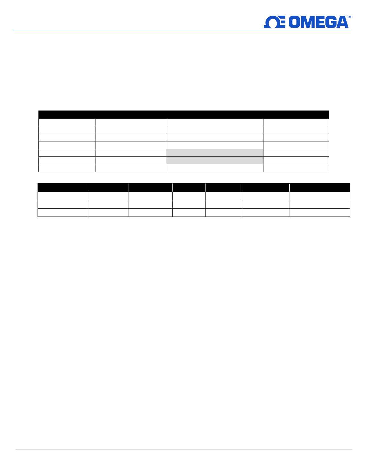
Type
Range
Resolution
Min
Max
Accuracy
Input Impedance
Current Loop
0-20 mA
± 0.1 mA
0 mA
24 mA
± 0.2 mA
50 ohm
Voltage
0 – 1.0 VDC
± 10 mV
0 VDC
1.20 VDC
± 10 mV
100k ohm
Voltage
0 – 2.0 VDC
± 10 mV
0 VDC
2.50 VDC
± 20 mV
100k ohm
Type
Range
Operating Conditions
Accuracy
Frequency (Rate)
0.01 Hz to 100 Hz
T
PW MIN
= 200 uS
± 0.5%
Frequency (Rate)
100 Hz to 1000 Hz
T
PW MIN
= 200 uS
± 1 Hz Averaged over 1s
Up Counter
0 to +8388608
1 kHz Max Rate
± 1 Count Max
Up/Down Counter
-8388608 to +8388608
1 kHz Max Rate
± 1 Count Max
Pulse Width (TPW)
200 uS min
± 50 uS ± 1%
Pulse Delay (TPP)
200 uS min
± 50 uS ± 1%
Duty Cycle
1% to 99%
0.01 Hz to 1000 Hz, T
PW MIN
= 200 uS
±1.5% Max
INPUT POWER
Voltage: 2.8 VDC - 3.3 VDC
DIGITAL INPUT SIGNALS
ON: 1.0 VDC
OFF: 0.7 V
Internal Pull Up/Down: 1.5k to 3.0 V
Comparator (PULSE) Input: 100 mV, 500 mV, 1.0 V
ANALOG (PROCESS) INPUT SIGNALS
DC
DC
, 2.0 V
DC
DC
DIO DIGITAL INPUTS
VinHighThreshold = 2.2 VMAX
VinLowThreshold = 0.3 VMIN
VinMAX = 30 VDC
DIO DIGITAL OUTPUTS
2x Open Drain 100 mA max
VMAX = 30 VDC
ENVIRONMENTAL
Operating Temperature: -40 to 85°C (-40 to 185°F)
Rating: IP67 when mated
MECHANICAL
Dimensions: 22.1 mm W x 96.7 mm L (0.87” x 3.80”) not including mounting tabs
GENERAL
Agency Approvals: CE, UKCA
Compatibility: Compatible with OEG, SYNC configuration software, Layer N Cloud, and Modbus Networks
7 | M5751
Page 8
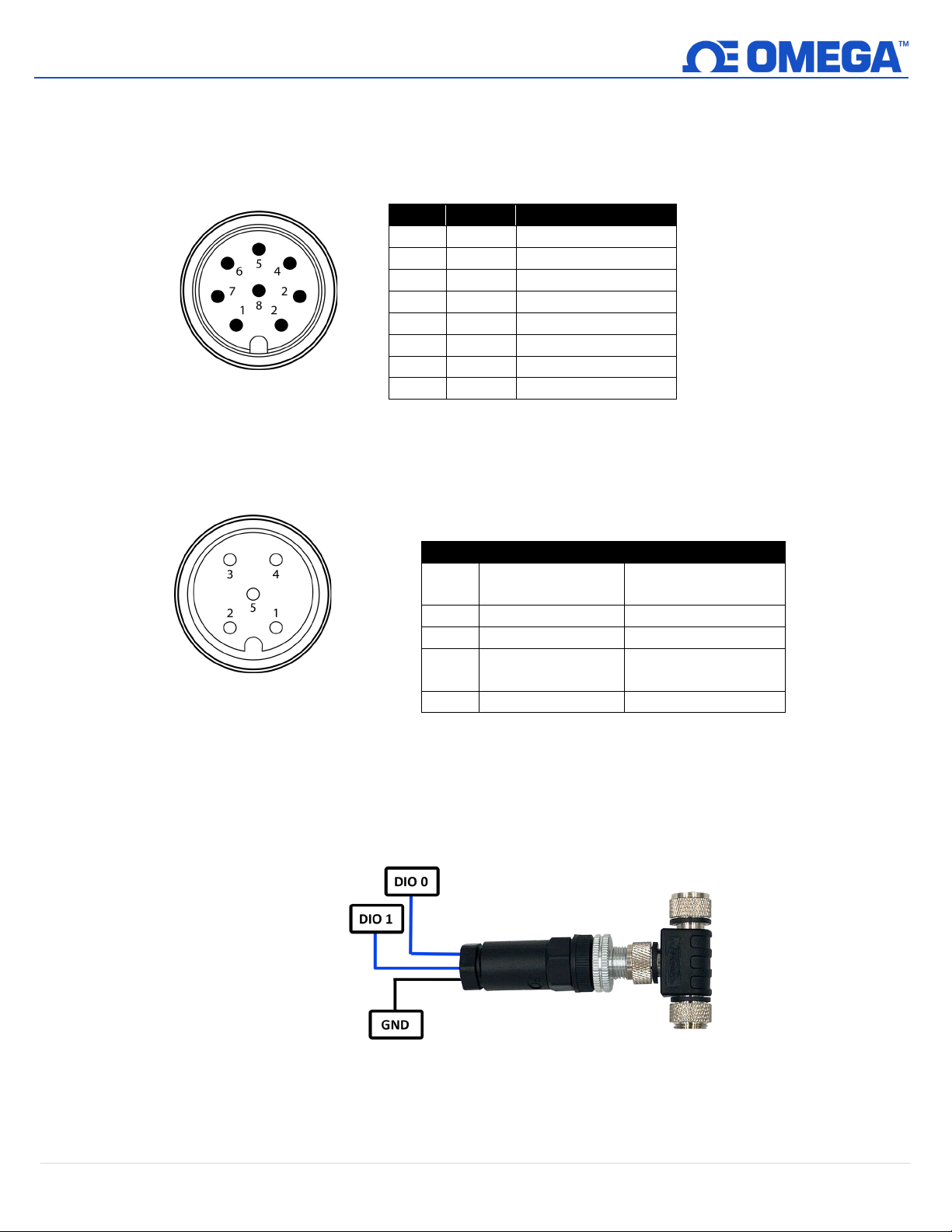
4 Hardware Setup
Pin
Name
Function
Pin 1
DIO 0
Discrete I/O Signal 0
Pin 2
INTR
Interrupt Signal
Pin 3
SCL
I2C Clock Signal
Pin 4
SDA
I2C Data Signal
Pin 5
Shield
Shield Ground
Pin 6
DIO 1
Discrete I/O Signal 1
Pin 7
GND
Power Ground
Pin 8
3.3VDD
Power Supply
Pin
Digital Mode
Mixed Mode
Excitation Power
(3.3 VDC, 100 mA)
Excitation Power
(3.3 VDC, 100 mA)
Pin 2
DIN 0 / Pulse A
DIN 0 / Pulse A
Pin 3
Ground Reference
Ground Reference
DIN 2 / Enable /
Direction / Pulse B
Pin 5
DIN 1 / Reset
DIN 1 / Reset
Figure 3: M12 8-Pin Male
Figure 4: M12 5-Pin Female
4.1 Connecting to your Layer N Smart Interface
The SP-013 requires a Layer N Smart Interface to connect to a computer. Use the M12 8-Pin Connector diagram
below to connect the SP-013 to a Layer N Smart Interface.
Connector Front View
4.2 Digital Input Wiring Diagram
The Layer N SP-013 accepts digital pulse inputs through its M12 5-Pin connector and a single process input in the
mixed input mode. Users connecting wires directly to the SP-013 may refer to the wiring diagram provided below:
4.3 Discrete I/O
If the smart probe discrete I/O will be utilized, an M12.8-T-SPLIT and an M12.8-S-M-FM will need to be connected
between the Smart Interface and Smart Probe. Refer to the previous pin diagram and the wiring diagram below to
connect the accessories:
Connector Front View
Pin 1
Pin 4
Process 0
Figure 1: M12.8-T-SPLIT and M12.8-S-M-FM accessories for Discrete I/O access
8 | M5751
Page 9
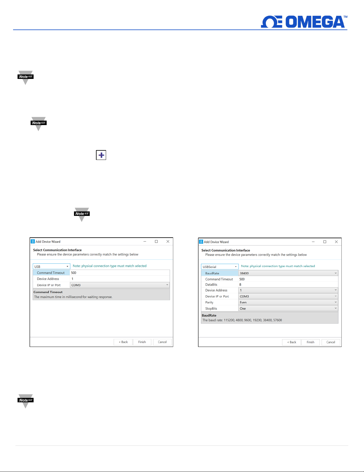
5 SYNC Configuration
Figure 2: USB Communication Interface
Figure 3: USB Serial Communication Interface
Layer N Smart Probe products are easily configured through Omega’s free SYNC configuration software. Ensure SYNC
is running on a Windows OS computer before continuing. Connect the SP-013 to the computer using your Layer N
Smart Interface to begin.
Note: SYNC is available to download for free on the OMEGA website.
5.1 Connecting to SYNC - Automatic Detect
Once the SP-013 and Layer N Smart Interface are connected to the computer, SYNC will automatically detect the
probe and begin displaying readings.
Note: If living readings from the SP-013 are displayed on SYNC, skip ahead to section 5.3 Input Configuration.
5.2 Connecting to SYNC – Manual
If SYNC does not automatically detect the device, follow these instructions to manually connect it.
Step 1: Click on the icon located on the top left of the SYNC interface.
Step 2: Proceed through the Add Device Wizard and click End Device / Probe.
5.2.1 Communication Interface
Set the communication parameters for the Layer N Smart Interface that you are connecting to.
Note: The connection type and parameters must be accurate for a proper connection to be
established. Failure to accurately setup communication parameters may result in
communication errors.
• Connection Type: Select the type of connection you have between your SP-013 and your computer.
• Command Timeout: The maximum time (in milliseconds) for a command to be completed before the command is
aborted.
Note: The default command timeout is 500 milliseconds. It is recommended that this section be left alone to avoid
communication errors.
9 | M5751
Page 10

• Device Address: If your Smart Interface is part of a network, enter the Network Address here. The default network
address is 1 for most devices. Please refer to the manual of your Smart Interface for more
information.
Note: The default Device Address is 1.
• Device IP or Port: The COM port number that your device is connected to on your computer.
Important: The following parameters should NOT be changed. These settings should NOT be changed unless the
configuration has been done on the interface.
• BaudRate: Controls bits per second
• DataBits: The number of ‘bits’ in each character sent.
• Parity: A means of checking the correctness of character by adding an extra ‘bit’ to the character and setting the
value based on all the other bits in the character.
• StopBits: The number of ‘bits’ used to indicate the end of the character.
Once you have completed setting the communication parameters for your device, click Finish.
10 | M5751
Page 11
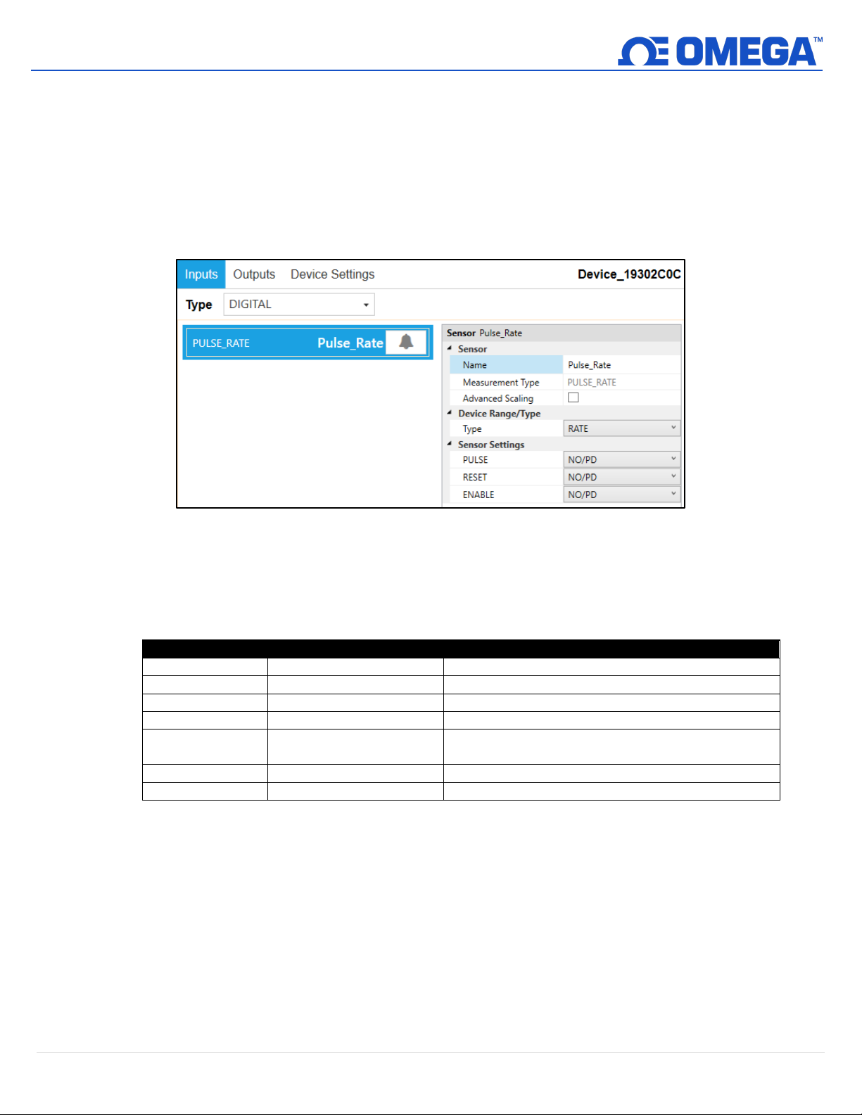
5.3 Input Configuration
Selection
Measurement
Description
DIN
Digital Input
3-bit Binary Digital Input
RATE
Frequency
Measure the frequency of rising edges
WIDTH
Pulse Width
Measure the active time of a signal
DUTY
Duty Cycle
Measure the % of active time of a signal
Measure the time between the rising edges of Pulse A
and Pulse B
COUNT
Up Counter / Totalizer
Counter with Enable and Reset
UP/DOWN COUNT
Up/Down Counter/Totalizer
Counter with Direction and Reset
Figure 7: SYNC interface digital input without DIO configuration
In Digital Inputs mode, the SP-013 accepts digital pulse inputs and may be configured to monitor the on/off state of
the input signals, the pulse rate or pulse duty cycle of the primary input, the up/down count of the primary input, or
the pulse delay between two signals. In Mixed Input mode, the SP-013 can accept one process input and one digital
pulse input. In all modes, the general Discrete I/O may be configured. These modes are detailed in the sections
below.
5.3.1 Digital Inputs Interface
To configure the Digital Inputs, follow the steps below:
Step 1: Click the Inputs configuration tab on SYNC and choose Digital or Digital, DIO from the Type dropdown.
Step 2: Select the type of digital input in the Device Range/Type dropdown in SYNC. The following types are
available:
DELAY Phase Delay Timer
11 | M5751
Page 12
Digital Input Binary
DIN_0
Inactive
Active
Inactive
Active
Inactive
Active
Inactive
Active
DIN_1
Inactive
Inactive
Active
Active
Inactive
Inactive
Active
Active
DIN_2
Inactive
Inactive
Inactive
Inactive
Active
Active
Active
Active
Digital_Input
Display (Binary)
Frequency (RATE) = Total
Frequency (RATE) = 1/pulse period if
Pulse Width
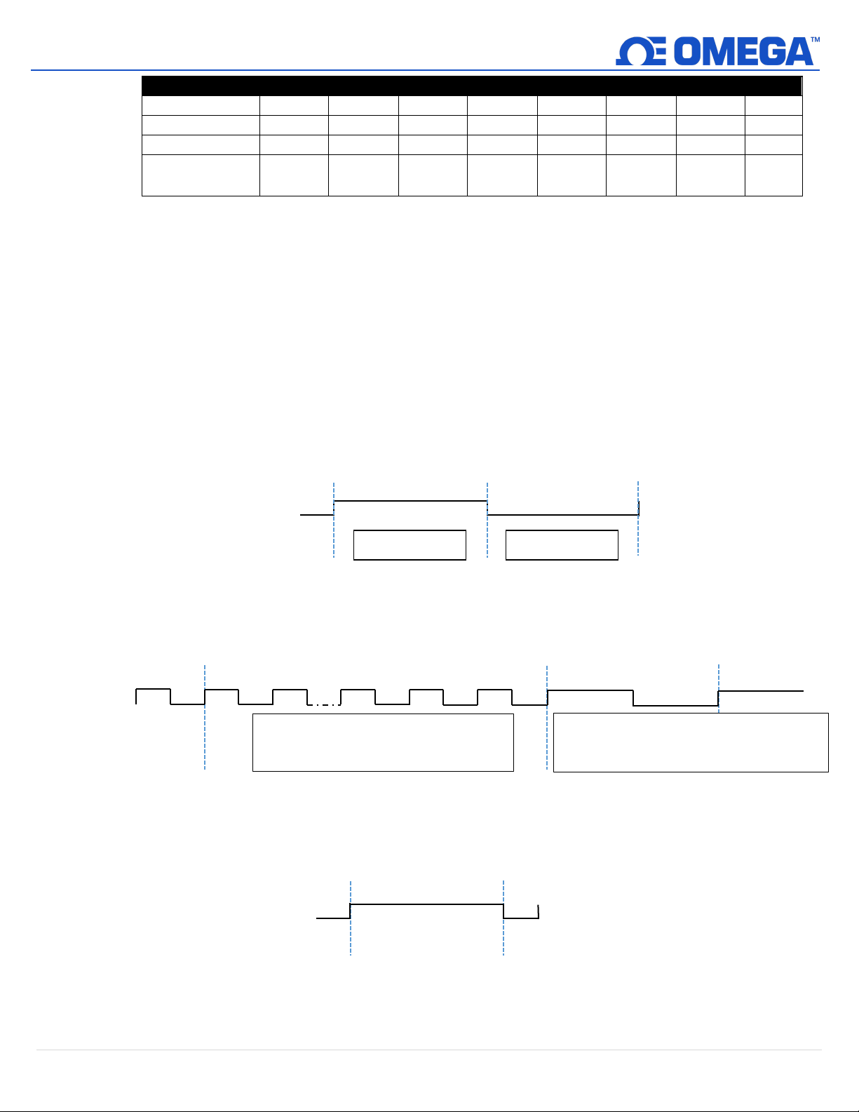
Figure 9: Frequency (rate) example
Figure 10: Positive pulse width example
Figure 8: Digital Input example
Digital Value 1
Digital Value 0
0.0 1.0 2.0 3.0 4.0 5.0 6.0 7.0
5.3.1.1 Pulse Measurements
Pulse measurements include Digital Input (DIN), Frequency (RATE), Pulse Width (WIDTH), Duty Cycle (DUTY),
Phase Delay Between Pulse Inputs (DELAY), Up Counter/Totalizer (COUNT), and Up/Down Counter/Totalizer
(UP/DOWN COUNT). All measurements are derived from signal transitions and an internal 32.768 kHz time
reference. The pulse input signal is read on the Pulse A input (pin 2) and the reset input signal is read on the
Reset input (pin 5). The third input on pin 4 changes its functionality depending on the pulse measurement
type and can be Enable, Direction, or Pulse. When the reset input is activated then the pulse input value is
zeroed for all pulse measurement types. When the third input pin is configured as an enable input and is
deactivated then the pulse input value is zeroed. Unless otherwise stated, the third input pin defaults to
Enable functionality which must be set HIGH to allow measurement.
The Digital Input (DIN) mode reports the binary value on the DIN pulse input pins. Note the DIN inputs
replace the functionality of the Pulse, Reset, and Enable inputs.
Two measurement modes are used when measuring Frequency (RATE). If the measured frequency is
greater than 100 Hz the total number of pulses/second is used to determine the frequency. If the measured
frequency is less than 100 Hz the time between rising edges is used to calculate the frequency.
Count/second if > 100 counts/second
frequency < 100 counts/second
The Pulse Width (WIDTH) setting measures the active portion of a periodic signal in msec. The pulse input
may be configured to be active high or active low to measure the positive or negative portion of the pulse
width. See the Input Configuration Diagrams section for details.
12 | M5751
Page 13
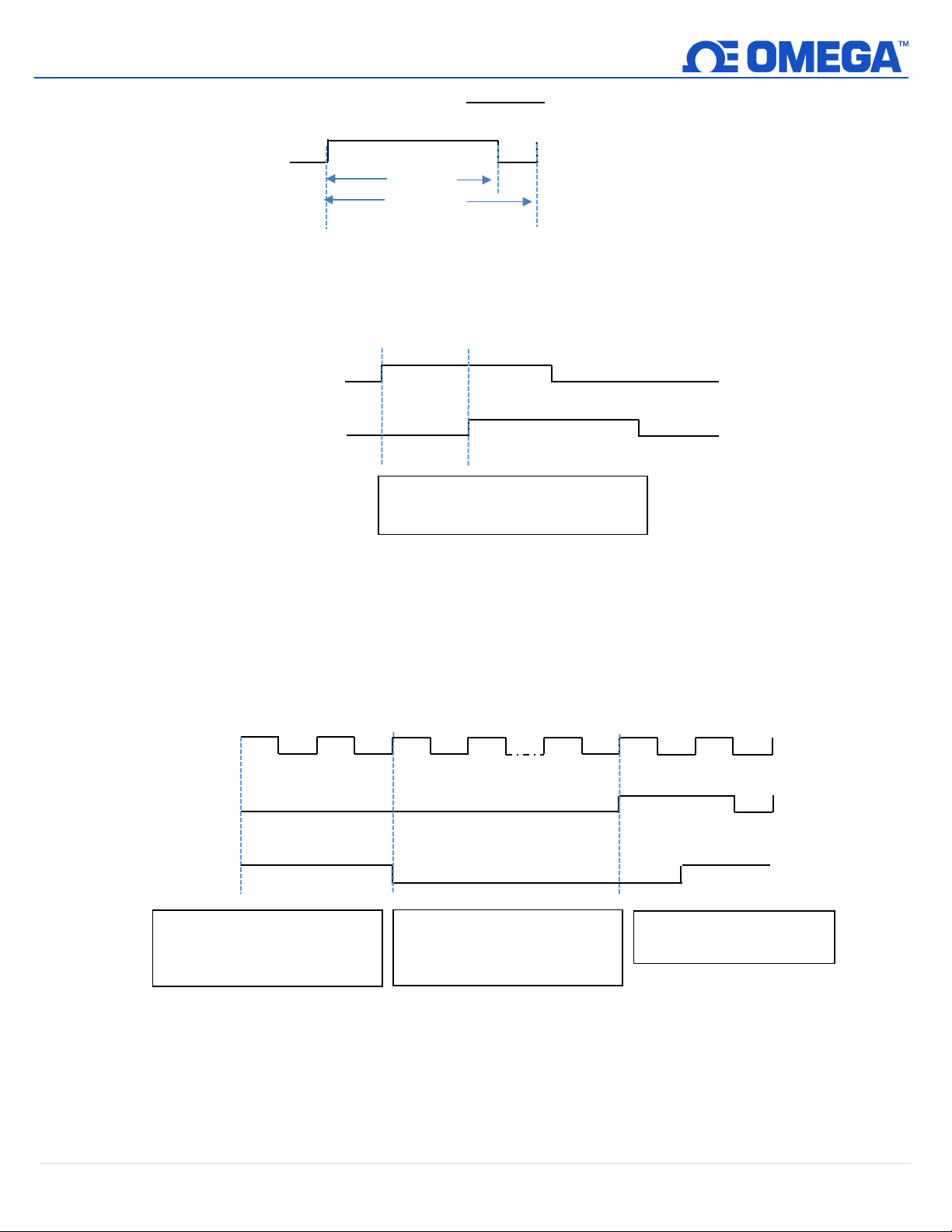
The Duty Cycle (DUTY) setting measures the percentage of time a pulse is active (high) over the total period
Duty Cycle = X / Y %
X
Figure 11: Duty cycle example
PULSE
RESET
Counts the number of pulses
Enable is active
Figure 13: Up Counter/Totalizer example with Active High Reset and Enable
Counter resets to 0 when
reset is active
PULSE_B
Measure the time between rising
Figure 12: Phase Delay example
ENABLE
Pauses the number of pulses
Enable is inctive
PULSE_A
of the signal. The duty cycle measurement allows reading the input from PWM control signals.
Y
Th
e Phase Delay (DELAY) mode measures the delay time in msec between the rising edges of Pulse A and
Pulse B inputs. Note the Pulse B input replaces the functionality of the Enable input. This function is
intended to be used on two input pulses operating at the same frequency but with different phase offsets.
edges of PULSE_A and PULSE_B
The Up Counter/Totalizer (COUNT) mode counts the number of rising edges while the Enable input is active
until the Reset input is activated. The Enable Input (Pin 4) acts as a Stop/Start for the Up Counter when
pulled up to 3.3 V. If the Enable Input is Inactive, it will pause/stop the up counter until it is re-enabled. If
the Enable Input is Active, it will start the up-count. Activating the Reset input (Pin 5) will reset the counter
back to 0. The Reset and Enable inputs can be configured to be active high or active low by configuring the
Enable Input to Pull-Down (PD). See the Input Configuration Diagrams section for details.
while Reset is inactive and
while Reset is inactive and
13 | M5751
Page 14
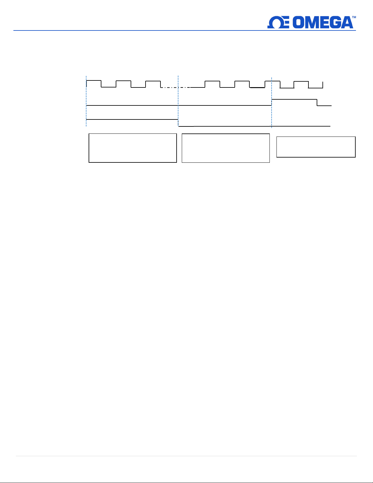
The Up/Down Counter/Totalizer (UP/DOWN COUNT) mode counts the number of rising edges until the
PULSE
RESET
Counts up the number of
and direction is active
Figure 14: Up/Down Counter/Totalizer example with Active High Reset and Direction
Counter resets to 0 when
reset is active
DIR
Counts down the number of
and direction is inactive
Reset input is activated. Additionally, the direction of the counter may be controlled using the Direction
input (Pin 4) so that it counts up when Active and down when Inactive. Note the Direction input replaces the
functionality of the Enable input. The Reset and Direction input can be configured to be active high or active
low. See the Input Configuration Diagrams section for details.
pulses while reset is inactive
pulses while reset is inactive
14 | M5751
Page 15
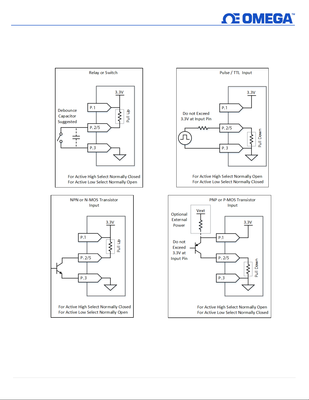
5.3.1.1.1 Input Configuration Diagrams
Figure 15: Active High/Low Circuit Examples
The digital pulse input pins can be independently set to either have an internal 1.5k Pull Up (PU)
or Pull Down (PD) and can be set to be either Active High or Active Low by selecting Normally
Open (NO) or Normally Closed (NC) in the SYNC input configuration interface. Some typical
circuits are shown below:
15 | M5751
Page 16
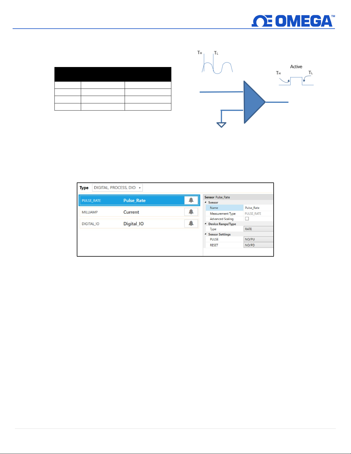
The DIN 0 / Pulse A input pin may also be configured for low-level mV input signals. The four selectable ranges
High Threshold
(ON)
Low Threshold
(OFF)
100 mV
75 mV
37.5 mV
500 mV
375 mV
187.5 mV
1.0 V
0.75 VDC
0.375 VDC
2.0 V
1.5 VDC
0.75 VDC
Figure 16: Active High/Low Threshold example
determine the turn-on threshold (TH) and the turn-off threshold (TL) which are used to set the ACTIVE level of
the digital input.
Setting
5.3.2 Mixed Input Interface
When set to the mixed input mode, the SP-013 can accept one process signal and one digital pulse input. To
configure the digital pulse and process inputs, follow these steps:
Figure 17: SYNC interface digital and process configuration with general DIO
Step 1: Click the Inputs configuration tab on SYNC and choose the Digital, Process or Digital, Process,
DIO type from the Type drop-down.
Step 2: For each respective channel, select the type of digital or process input in the Device
Range/Type drop-down. Click Apply Settings when done.
For additional information regarding pin wiring for the single digital and single process mixed mode, refer to
the wiring diagrams on page 8.
16 | M5751
Page 17
5.3.2.1 Digital Inputs (Mixed Mode)
Selection
Measurement
Description
DIN
Digital Input
2-bit binary digital input
RATE
Frequency
Measures the frequency of rising edges
WIDTH
Pulse Width
Measures the active time of a signal
DUTY
Duty Cycle
Measures the % of active time of a signal
COUNT
Up Counter / Totalizer
Counter with Enable and Reset
Input 1
Input 0
Reading
Inactive
Inactive
0
Inactive
Active
1
Active
Inactive
2
Active
Active
3
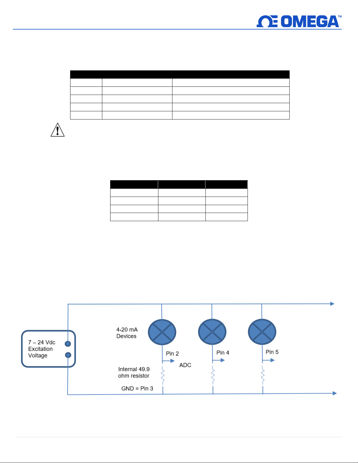
Figure 18: 4-20 mA device connection diagram
The following table lists the available digital input configuration options available when in mixed mode.
Some options available in digital-only mode are not available in mixed mode. Descriptions and example
diagrams are provided starting in section 5.3.1.1 Pulse Measurements.
Important: Digital input signals (pulse inputs) must be referenced to ground when Mixed Mode is used.
Negative offsets at pulse inputs may cause interference and noisy/incorrect readings in
analog (mA/V) process input signals.
The table below shows the binary-weighted values for the 2-bit Digital Input (DIN) function in mixed
mode.
5.3.2.2 Process Inputs (Mixed Mode)
The following process input configuration options are available in mixed input mode: 4-20 mA current loop,
0-1.0 V voltage input, 0-2.0 V voltage input. Current loop readings are rounded to the nearest 0.1 mA and
voltage readings are rounded to the nearest 10 mV.
5.3.2.2.1 4-20 mA Device Connection
The Current Loop interface measures the current into the selected input by converting it to a
voltage measurement across a fixed 49.9-ohm resistor.
17 | M5751
Page 18
5.3.3 Discrete Input/Output (DIO)
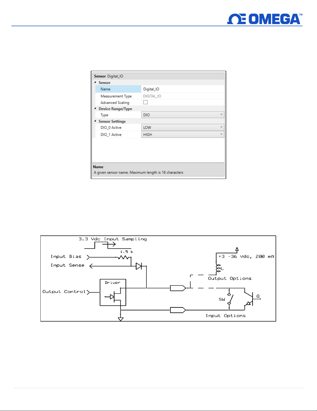
Figure 19: SYNC interface discrete I/O input configuration
Figure 20: Digital/Discrete I/O circuitry
The Layer N SP-013 features 2 configurable discrete I/O pins. These can be used for a myriad of applications
including driving relays, physical alarms, or sensing dry contacts like door switches. The user may configure
the polarity of the inputs (active HIGH or active LOW) or Disable the DIO to utilize the outputs (ON/OFF,
PWM, SERVO).
The Discrete I/O input shares the output circuitry. The internal process drives the output control signal to
turn on the output driver which will force the output low. When the state of the DIO input signal is to be
read the processor applies 3.3 V
to the Input Bias signal and reads the level detected at the Input Sense. If
DC
the output is inactive an external signal may be used to force the input level low. A diode protects external
positive voltages, allowing the output driver to activate loads greater than the internal 3.3 V
DC
.
18 | M5751
Page 19
5.3.3.1 Setting DIO as an Input
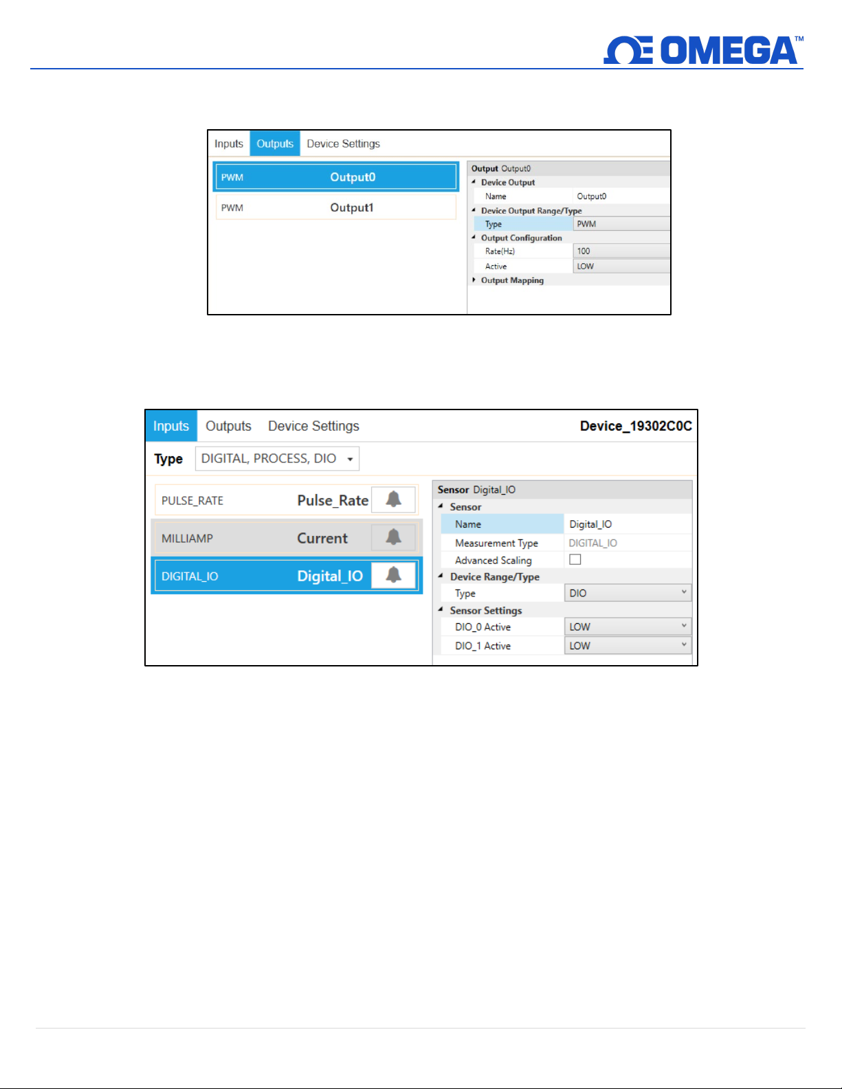
Figure 21: SYNC interface outputs tab
Figure 22: SYNC interface Digital_IO
To use a DIO pin as an input, make sure it is set to Active Low (default) in the Output Tab in SYNC.
Then, in the Input Tab, select a Type from the drop-down which includes DIO. Each DIO pin has an internal
pull-up, but to save power, the internal pull-up is only active when the unit takes a reading.
5.3.4 Advanced Scaling Options
The Layer N SP-013 allows for advanced scaling options on process and pulse inputs only. The Advanced
Scaling checkbox can be selected to expand additional configuration options. A gain and/or offset can be
applied to the input reading and the displayed unit can be changed.
To apply a gain or offset to the input, expand the Scaling menu and ensure that Apply Scaling is checked.
There, the gain and offset values can be adjusted. Both positive and negative values may be entered as well
as decimal numbers. The equation for the scaled input value is given below.
The displayed units can be changed by entering a new value in the Unit field and clicking Apply Settings.
This field is limited to a maximum of 4 characters. Note that changing the Unit field does not change the
base unit type, only the display name. The Lock checkbox must be selected to use the user-defined Unit
field. Unchecking the Lock checkbox and clicking Apply Settings will revert the unit display back to the
default setting.
=
(
× )+
19 | M5751
Page 20
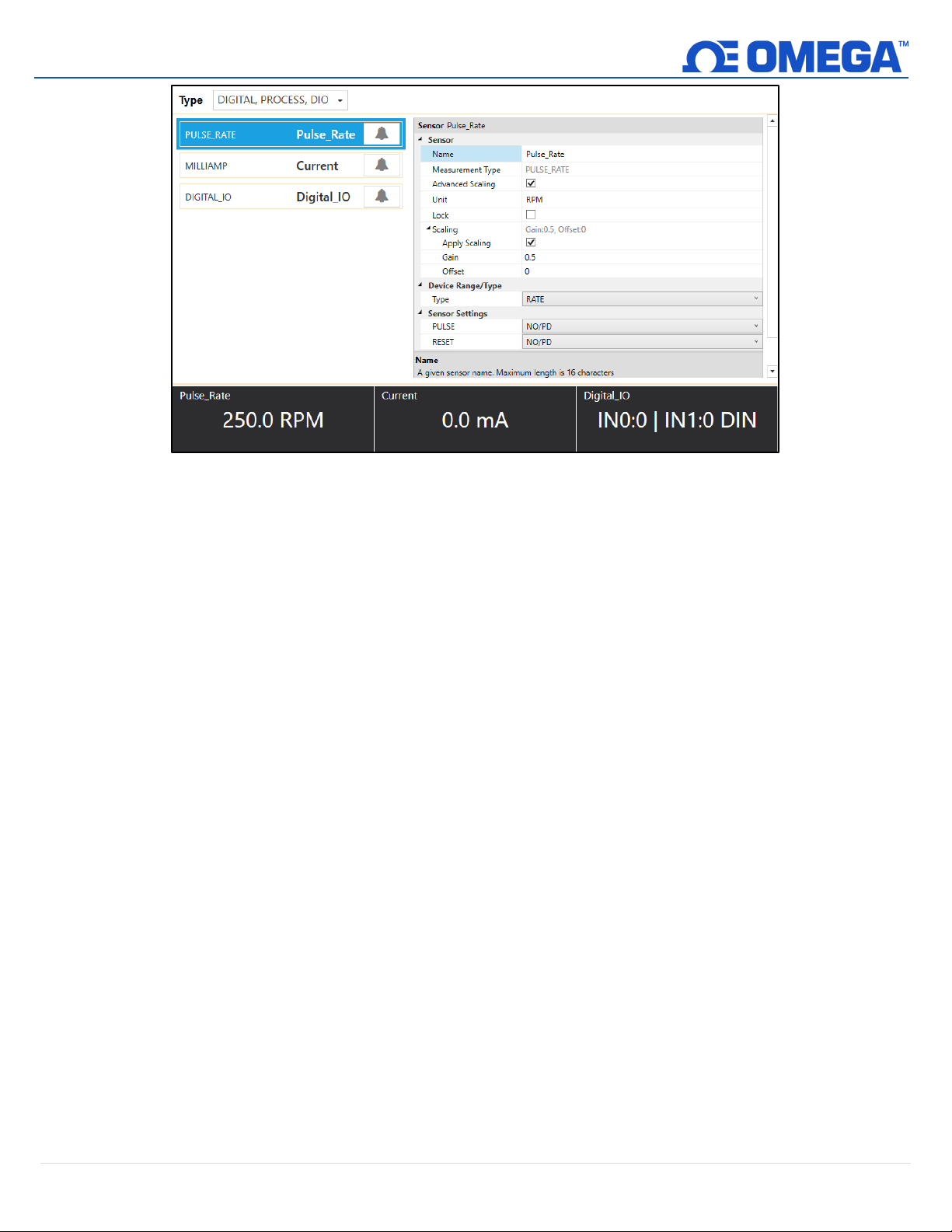
Figure 23: Advanced Scaling Example
The screenshot above shows an example application for advanced scaling with changed units. A fan tachometer
with a 500 Hz signal is connected to the Pulse Rate input. The fan outputs 2 pulses per revolution, so to convert
to rotations per minute (RPM) the reading must be divided by 2 which is accomplished by setting the Gain to
0.5. The units can then be renamed to RPM and will display as such.
20 | M5751
Page 21
5.4 Output Configuration
Option
Value
Description
LOW
When the output is inactive, it is in a high impedance state.
HIGH
When the output is active, it is in a high impedance state.
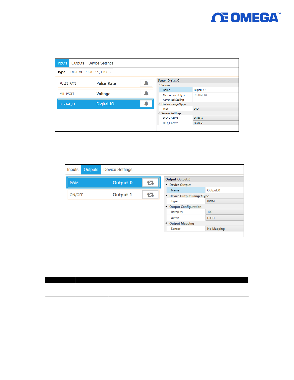
Figure 24: SYNC interface SP-013 DIO_0 and DIO_1 set to Disable
Figure 25: SYNC interface Output Configuration
The SP-013 offers two discrete outputs that share circuitry with the discrete inputs. If an output is to be used then
the corresponding input pin must be set to Disable. See section 5.3.1 Discrete Input/Output (DIO) for more
information.
There are three types of output options – On/Off, Pulse-Width Modulation (PWM), or Servo. See section 5.4.1 for
more information on each type.
Outputs may be configured as either Active High or Active Low. When configured as Active High the output conducts
normally and becomes high impedance when activated. When configured as Active Low the Open-Drain output is
high impedance normally and will conduct when activated.
Active
An output may be controlled in one of three ways – a scaled mapping to an input, an on/off control from an input
setpoint, or as an input alarm. Sections 5.4.2 through 5.4.4 describe these output control methods.
21 | M5751
Page 22
5.4.1 Device Output Range/Types
Option
Value
Description
100 Hz
Signal has a constant 100 Hz frequency with 0-100% Duty Cycle
10 Hz
Signal has a constant 10 Hz frequency with 0-100% Duty Cycle
1 Hz
Signal has a constant 1 Hz frequency with 0-100% Duty Cycle
0.1 Hz
Signal has a constant 0.1 Hz frequency with a 0-100% Duty Cycle
Active LOW
When the output is active, it is pulled to ground (LOW)
Active HIGH
When the output is active, it is in a high impedance state
Option
Value
Description
100 Hz
Signal has a constant 100 Hz frequency
50 Hz
Signal has a constant 50 Hz frequency
Pulse Width
Range
1.0-2.0 msec
On time varies between 1 and 2 msec
0.5-2.5 msec
On time varies between 0.5 and 2.5 msec
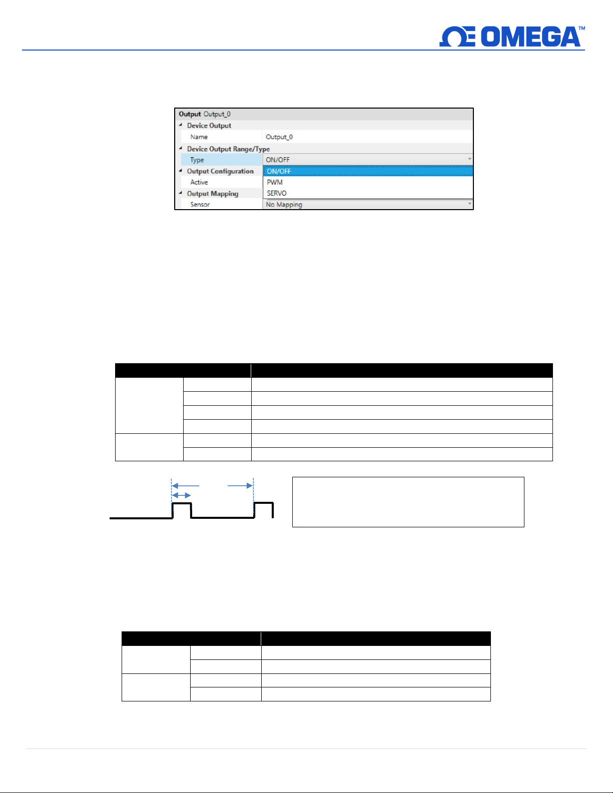
Figure 26: SYNC interface output type selection
20 % Duty Cycle
Example shows a PWM output signal configured
100 Hz
Figure 27: PWM function diagram
There are three types of output options – On/Off, Pulse-Width Modulation (PWM), or Servo. This section
describes these output options.
5.4.1.1 ON/OFF Output Type
The ON/OFF output mode switches the output to be a binary ON or OFF. Depending on if the output is
configured as Active Low or Active High, the ON/OFF mode can correspond to different polarities.
5.4.1.2 Pulse-Width Modulation (PWM) Output Type
Pulse-Width Modulation (PWM) controls the amount of power given to a device by cycling the on/off
phases of a digital signal. PWM consists of a duty cycle and frequency. The Duty Cycle measures the amount
of time a signal is in the ON state as a percentage. The frequency controls how fast the PWM cycle is
repeated. Users can select between the following settings:
Rate
Signal Type
5.4.1.3 SERVO Output Type
The SERVO output allows driving servo motors that control position. A Servo output is a special case of the
PWM output, where the ON time varies between 1.0 msec and 2.0 msec or between 0.5 msec and 2.5 msec,
with the lower bound representing 0 degrees and the upper bound representing 180 degrees of angular
travel. The typical non-critical frequency is 50 or 100 Hz. Servo outputs are always active high.
Rate
with a 100 Hz frequency and active HIGH
outputs. The duty cycle has been set to 20%.
22 | M5751
Page 23
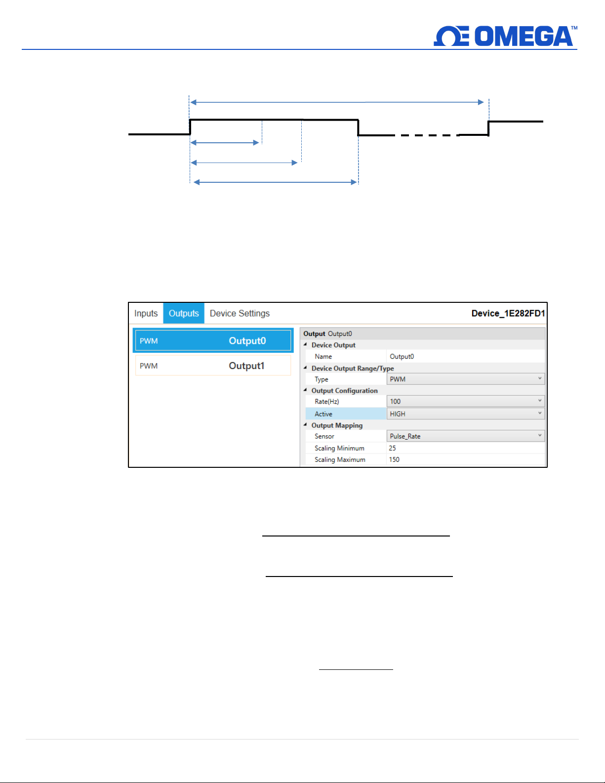
Example: For the percent of angular travel, if the pulse width range is set to a range of 1.0-2.0 msec, then
Figure 29: Sensor output mapping configuration example
100% Angular Travel = 2.0 msec
50 Hz
Figure 28: SERVO output example
1.0 msec = 0°
1.5 msec = 90°
2.0 msec = 180°
selecting 50% of angular travel represents 1.5 msec or 90 degrees of travel.
5.4.2 Sensor Output Mapping
The SP-013 allows mapping a scaled copy of any of the input values to any of the outputs. To set a mapped
output, it must not be associated with any alarm or ON/OFF control module. Two user-defined values,
Scaling Minimum and Scaling Maximum, define the sensor range that is mapped to the output. A Factory
Reset sets the Input Minimum to 0 and the Input Maximum to 100.
The scaling equations for direct and reverse output percentages are given below.
Example: The figures below and above display a PWM output direct-mapped to a Rate input. The minimum
expected input rate is 25 Hz and the maximum expected rate is 150 Hz. A value of 50 Hz read at the input is
then mapped to a PWM output with an 80% duty cycle.
,
=
=
150 50
=
150 25
× 100% = 80%
× 100%
× 100%
23 | M5751
Page 24
5.4.3 ON/OFF Control Module
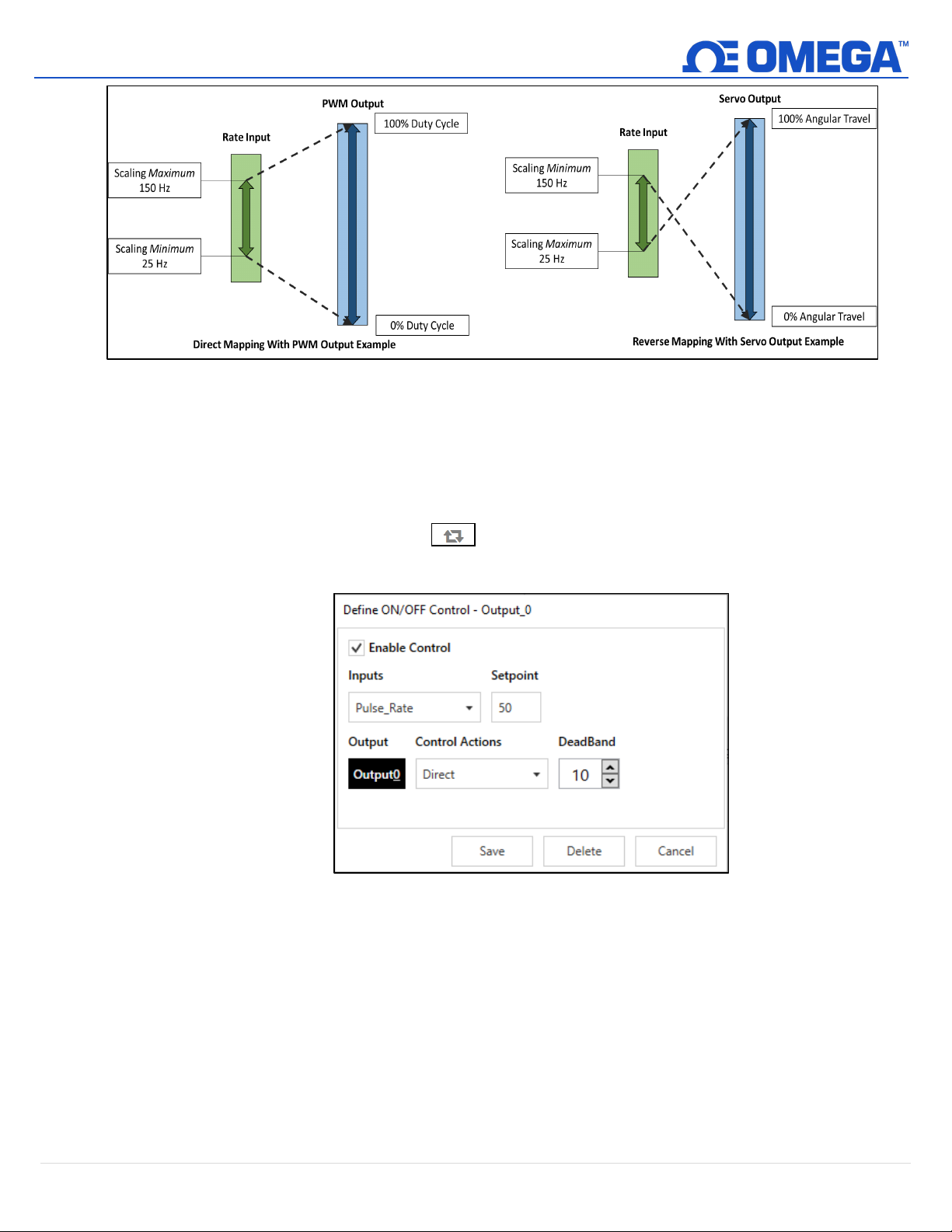
Figure 30: Sensor output mapping diagram
Figure 31: SYNC interface ON/OFF control module functions
To configure an ON/OFF control module on a device, first ensure that the desired output pin is not
associated with any input alarms and that it is set as No Mapping in the Output Mapping menu in the
Outputs tab. The ON/OFF control module can be used with any selected output type including ON/OFF,
PWM, and SERVO. When enabled in PWM mode, ON corresponds to 100% duty cycle. When enabled in
SERVO mode, ON corresponds to 100% angular travel.
In the Outputs Tab in SYNC click on the icon located to the right of the available outputs. Clicking the
icon will open the Define ON/OFF Control dialog box as seen below.
The Enable Control checkbox enables the ON/OFF control module. If this box is unchecked, the output will
be disabled but the module with all its settings will remain available to be enabled at a later time.
The Inputs dropdown lists the available input sources and will depend on how the device is configured in
the Inputs tab.
The Setpoint field sets the threshold for activating the ON/OFF control module. The unit of the Setpoint
field will be the same as the unit of the chosen Input.
The Control Actions dropdown has options for direct or reverse control. In direct mode, once the Setpoint
value is reached then the output will be set to ON. In reverse mode, once the Setpoint value is reached then
24 | M5751
Page 25
the output will be set to OFF.
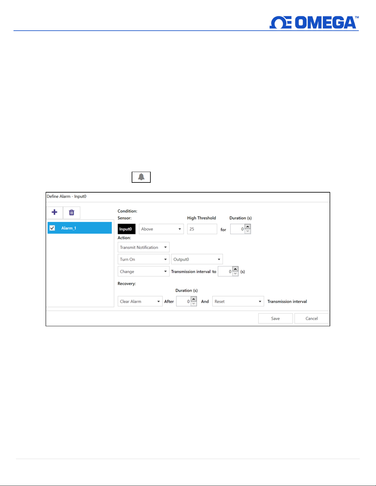
Figure 32: SYNC alarm configuration interface
The DeadBand field together with the direct or reverse control action configures a deadband range around the
Setpoint where the ON/OFF control does not toggle. The unit of the DeadBand field will be the same as the unit
of the chosen Input.
• Example 1: the setpoint is configured for a 50 Hz rate input with a deadband of 10 Hz with direct control
action. The output will activate if the input rises above 60 Hz. Conversely, the output will become
inactive if the input falls below 50 Hz.
• Example 2: the setpoint is configured for a 50 Hz rate input with a deadband of 10 Hz with reverse
control action. The output will activate if the input falls below 40 Hz. Conversely, the output will become
inactive if the input rises above 50 Hz.
The Save button saves and applies the configurations settings to the ON/OFF control module. The Delete button
only appears for a previously saved ON/OFF control module and it removes the module and allows other output
types to be configured such as an alarm or mapping.
5.4.4 Setting an Alarm
Alarms are set by clicking the icon in SYNC on the desired input signal found in the Input Tab.
Configure the Condition that triggers the alarm by selecting an option from the drop down such as Above or
Below. The Threshold field(s) will change to display whatever is appropriate for the option chosen such as a High
Threshold for an Above condition or a Low Threshold for a Below condition. A Duration can be set for the trigger
as well where the condition must be met for a certain amount of time before the alarm flags.
Under the Action menu, the option to transmit or not transmit a notification can be set. The option to enable an
output can also be set. The output chosen must not be currently used in a sensor mapping or ON/OFF control
module. The data transmission interval may also be changed upon triggering an alarm, e.g. increate the rate of
transmission if an excessive value is detected.
The Recovery menu allows the option to clear the alarm after a certain Duration once the trigger condition is no
longer met. The transmission interval can also be reset to the normal system setting once the alarm is cleared.
25 | M5751
Page 26
To create a new alarm, click the plus icon and a new alarm will be added. To remove an alarm once it is
created, select the alarm in question on the left side of the alarm panel and click the delete icon .
6 Pairing a Sensing Device to a Layer N Gateway
Refer to either the Wired or Wireless instructions to pair a Layer N Smart Probe & Interface to a Layer N Gateway.
Before continuing to the pairing instructions, ensure the following prerequisites are met:
• Ensure that the Layer N Gateway has been properly setup, powered on, and in close physical proximity.
• (For Wired pairing) Ensure the user has access to a PC and the internal Gateway UI (refer to the Layer N Gateway
manual for instructions on how to access the internal Gateway UI).
6.1 Wireless Pairing
Pairing a wireless Smart Interface (IF-006) with probe attached is made easy with a one-button pairing system
between the IF-006 and the Layer N Gateway.
Step 1: When the Smart Probe and relevant accessories have been securely connected to the IF-006, push the
pairing button once on the IF-006. The LED status indicator will blink green indicating the device is in
Pairing Mode.
Step 2: Quickly push the pairing button on the Layer N Gateway. The LED on the Gateway will blink green indicating
the Gateway is in Pairing Mode.
When the IF-006 or Smart Sensor has been successfully paired to the Layer N Gateway, the LED will stop blinking on
both devices. Readings for the newly added device will then appear on the Layer Cloud or OEG interface.
6.2 Wired Pairing
Wired Smart Probes connected directly to a Layer N Gateway with an IF-001 cable or IF-002 will need to be added to
the Gateway Internal User Interface.
The Connected Devices tab is the default page set once you are signed in to the internal gateway UI. From here, you
can add devices to your gateway to have them appear in your Layer N Cloud account.
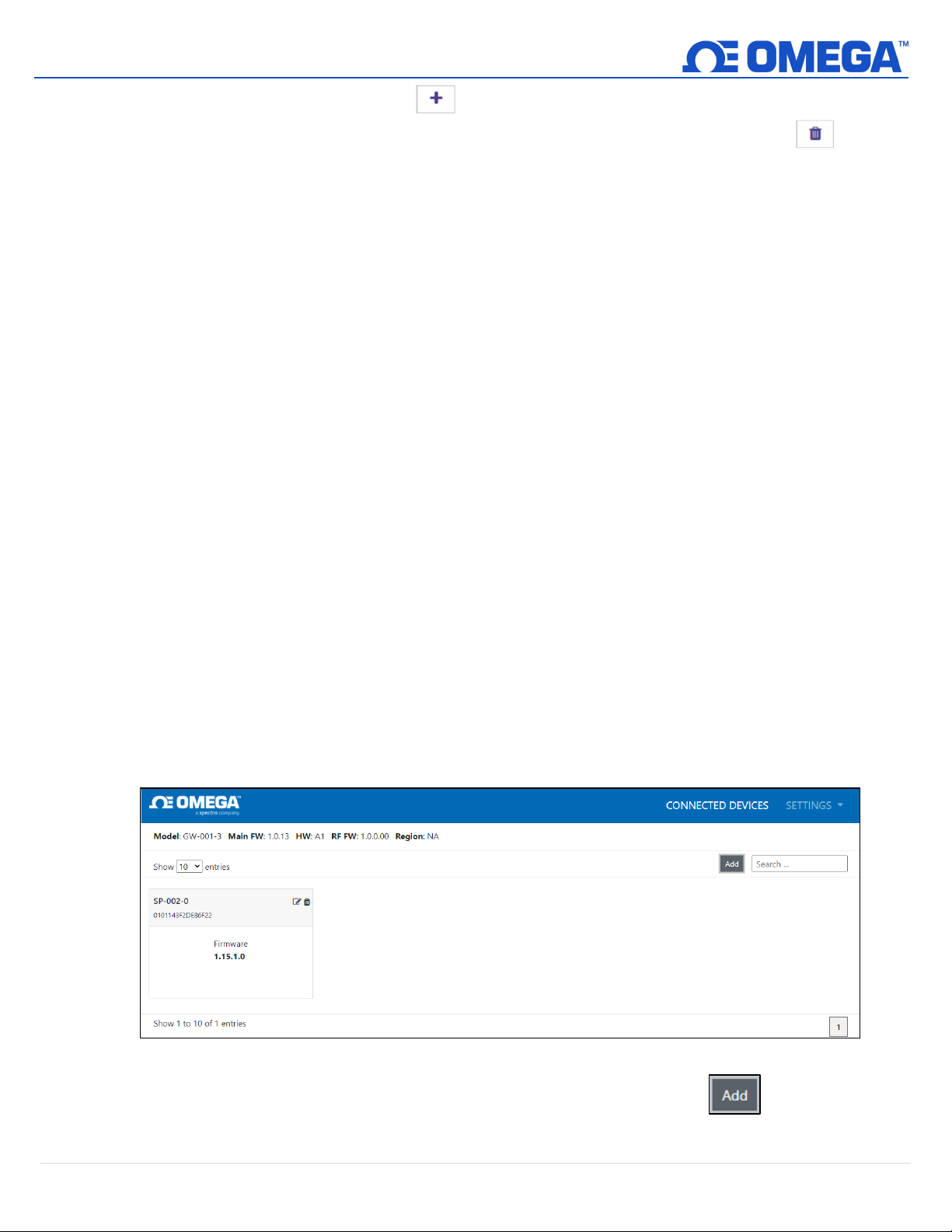
Figure 33: Gateway Internal User Interface
To add a device to your gateway from the internal gateway web UI, begin by clicking the button at the top
right of the web page. Fill out the Add Device menu with the parameters of the Smart Probe connection.
26 | M5751
Page 27
7 Appendix: SP-013 Registers
Enumerated Sensor
Digital
Mixed Mode
DIN, RATE, WIDTH, DUTY_CYCLE,
or COUNT
DIN, RATE, WIDTH, DUTY_CYCLE,
OR COUNT
1
0x0068 (0xf034)
0x09a8 (0xf4d4)
DIO
Process 0
2
0x0070 (0xf048)
0x0aa8 (0xf554)
Not Used
DIO
3
0x0078 (0xf03c)
0x0ba8 (0xf5d4)
Not Used
Not Used
Offset
Name
Value
Description
DIO, FREQUENCY, WIDTH, DUTY_CYCLE, DELAY, or
byte.
0x01
Data Type/Format
0x46
Float, Writeable
0x02
Configuration
0x??
Determines channel and Measurement Type
0x03
Sensor Device
0x??
Determines DIO signal types
0x04
UOMR
“??”
Units of measure
The following Appendix provides the registers and list index for the Layer N SP-013 Digital Input Smart Probe. This
information is intended to aid users who will be making configurations and adjustments to their Layer N SP-013 Digital
Input Smart Probe through the Command Line Interface or other custom interfaces.
Smart Probe devices share a common platform architecture that provides extensive monitoring and control
capabilities through a set of platform generic registers. These registers may be accessed using I2C based commands
directly to the Smart Probe devices or through a set of Modbus-based registers when using Omega Interface devices.
When powered on or after a device reset each Smart Sensor-based device will enumerate 1 or more sensor instances
which are described by the device-specific Sensor Descriptors which include configuration options, measurement type,
and units of measure for the corresponding sensor values. Additional sensor information is provided in sensor-specific
IPSO object descriptions which include extended measurement type, precision, and tracking of minimum/maximum
readings.
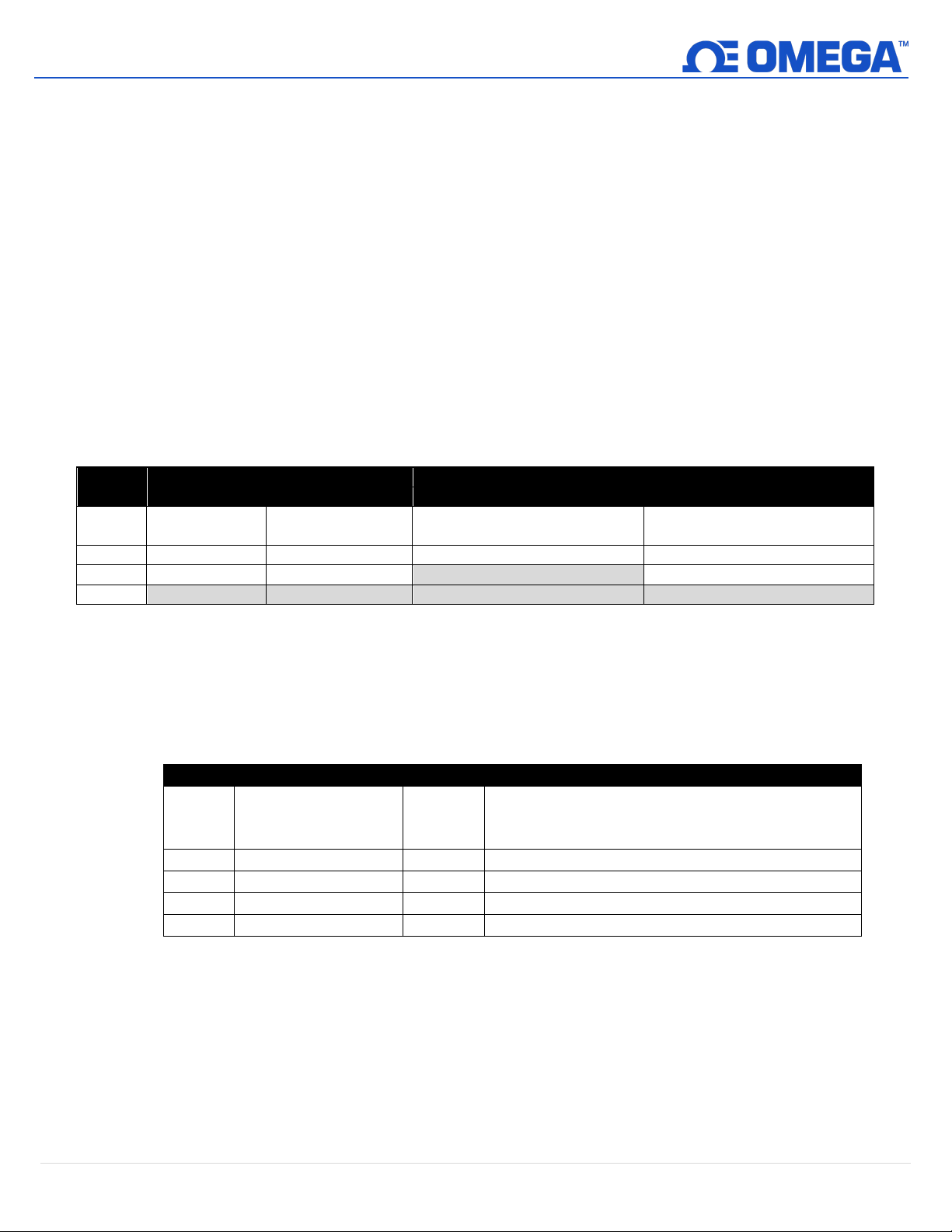
Each enumerated Sensor has a Descriptor Base address location and a Sensor IPSO /Configuration structure address
location based on the sensor mix selected.
Sensor Descriptor Base IPSO/Configuration
0 0x0060 (0xf030) 0x08a8 (0xf454)
7.1 Digital Descriptor
The SP-013 configures the sensors based on the factory device list and user-specified list index. The Sensor
Configuration and Sensor Device fields may be written to provide control of the overall function of the channel and
the signal types used.
7.1.1 Digital Descriptor
0x00 Sensor Type 0x??
COUNT – set by Sensor Type field in Configuration
27 | M5751
Page 28
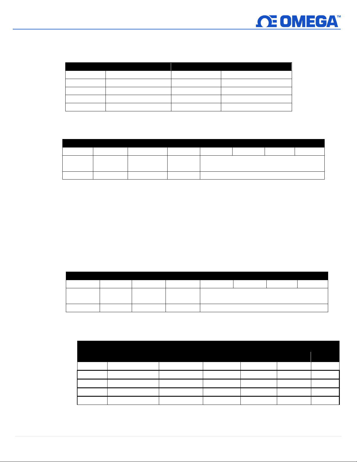
7.1.1.1 Digital Measurement Types
Sensor Type
Measurement
SI Derived Units
Measurement
0x18
DIN
DIN
DIN (Digital Inputs)
0x19
FREQUENCY (RATE)
Hz
RATE
0x1a
PUSLE WIDTH
msec
PULSE WIDTH
0x1b
DUTY CYCLE
%
DUTY CYCLE
0x1d
COUNTER
CNT
COUNTER
Digital Data Type/Format
7 6 5 4 3 2 1
0
Smart
Sensor
Factory
Calibrate
0 1 0
0
6 == Floating point
Digital Configuration
7 6 5 4 3 2 1
0
Apply
Scaling
0 0 ?
?
(See Below)
Signals
DIO2
DIO1 **
DIO0
0x00
DIO
0x18
DIN
INPUT 2
INPUT 1
INPUT 0
0x01
RATE
0x19
Hz
RESET
ENABLE
PULSE
0x02
PULSE WIDTH
0x1a
msec
RESET
ENABLE
PULSE
0x03
DUTY CYCLE
0x1b
&
RESET
ENABLE
PULSE
0x05
COUNTER
0x1d
CNT
RESET
ENABLE
PULSE
The Digital interface provides a measurement dependent on the input range/type selected. The units of
measure may be changed by the user.
7.1.1.2 Digital Data Type/Format
Writeable
7.1.1.2.1 Data Type
The 4-bit Data Type field determines the type of data of the specific sensor.
7.1.1.2.2 Factory Calibrate
No Factory calibration is used on the digital pulse inputs.
7.1.1.2.3 Writeable
The writeable bit is set, indicating that the sensor values may be overwritten. This allows values to
be preset, such as setting a counter value to 0.
7.1.1.3 Digital Configuration
Available Assigned
7.1.1.3.1 Sensor Range / Type
Reserved Data Type
Lock Sensor Range / Type
** When configured for Mixed-mode operation (Digital pulse + Process) the DIN1 signal is used for the
Process input signal. The Pulse Delay and Up/Down counter functions are not available.
Range / Type
Measurement
Type
Units of
Measure
28 | M5751
Page 29
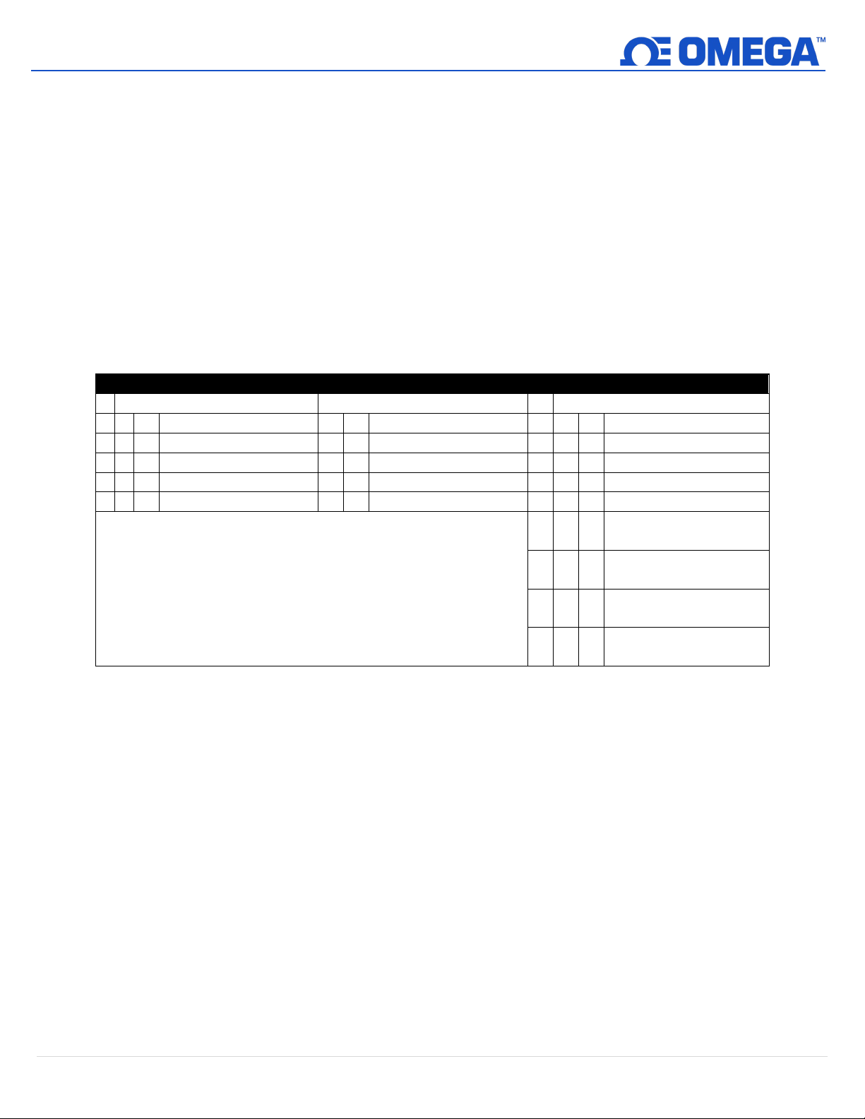
7.1.1.3.2 Lock
Digital I/O Device Byte
SIG 2 (ENABLE)
SIG 1 (RESET)
SIG 0 (PULSE)
7 6 5
Description
4 3 Description
2 1 0
Description
0 0 0
N.O. SINK (DRY)
0 0 N.O. SINK (DRY)
0 0 0
N.O. SINK (DRY)
0 0 1
N.C. SINK (DRY)
0 1 N.C. SINK (DRY)
0 0 1
N.C. SINK (DRY)
0 1 0
N.O. SOURCE (WET)
1 0 N.O. SOURCE (WET)
0 1 0
N.O. SOURCE (WET)
0 1 1
N.C. SOURCE (WET)
1 1 N.C. SOURCE (WET)
0 1 1
N.C. SOURCE (WET)
COMPARATOR
(100 mV)
COMPARATOR
(500 mV)
COMPARATOR
(1.0 V)
COMPARATOR
(2.0 V)
If set, the user-specified units of measure string (4 character maximum) will be used in place of
the default.
7.1.1.3.3 Apply Scaling
If set, the user-defined Offset and Gain values will be used to adjust the sensor reading:
7.1.1.3.4 Assigned
The Assigned bit will always read as 0.
7.1.1.3.5 Available
The Available bit will always read as 0.
7.1.2 Digital Input Device Byte
For digital input types, the Device Byte field determines the signal types for each of the channel bits.
Result = (Raw Reading * Gain) + Offset
7.1.3 Digital Sensor Parameters
There are no Digital Sensor Parameters.
1 0 0
1 0 1
1 1 0
1 1 1
29 | M5751
Page 30
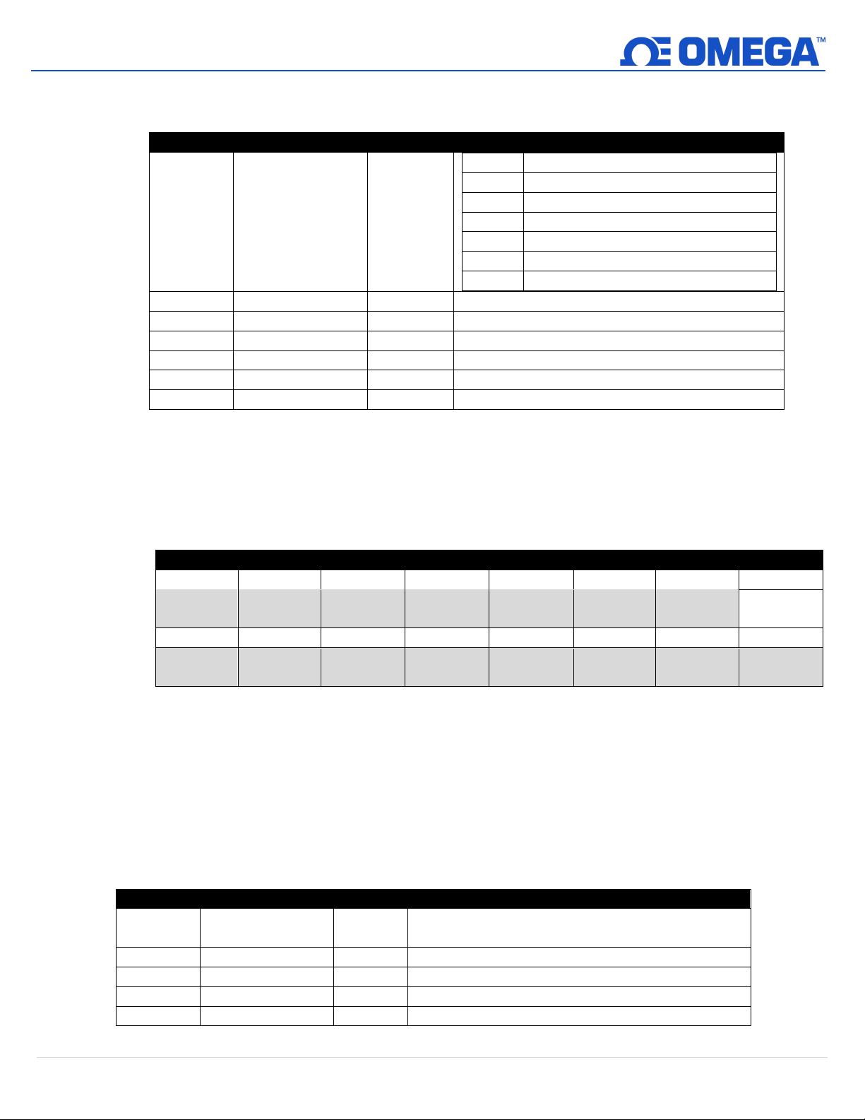
7.1.3.1 IPSO Digital Definition
Offset
Name
Value
Description
Value
Description
3318
Frequency
33005
Pulse Width
33006
Pulse Delay
33007
Duty Cycle
33002
Counter
33003
Up/down Counter
0x08aa
Precision
0
Provides reading of xxx
0x08ac
Sensor Trigger
??
See Below
0x08b0
Min Measured
??
Minimum reading since the last reset
0x08b4
Max Measured
??
Maximum reading since the last reset
0x08b8
Min Range
-8388607
Minimum reading
0x08bc
Max Range
+8388607
Maximum reading
Sensor Trigger Function
7 6 5 4 3 2 1
0
Reset
Min/Max
15
14
13
12
11
10 9 8
Calibration
Reset
Calibration
Status
Calibration
Mode
Capture
High
Capture
Low
Calibration
Start
Offset
Name
Value
Description
Measurement
Type
Analog Voltage and Current – set by Sensor Type
field in Configuration byte.
0x01
Data Type/Format
0x06
Float,
0x02
Configuration
0x4?
Determines Process input type/range
0x03
Sensor Device
0x??
Determines AIO signal types
0x04..0x08
UOMR
“??”
Units of measure
The IPSO Digital definition provides signal range, measured min/max values, IPSO object type information.
0x08a8 Sensor Type <table>
7.1.3.2 Digital Resolution
The measured digital value provides +/- 1.0 resolution.
7.1.3.3 Sensor Trigger Function
The Sensor Trigger function is used to reset the IPSO min/max values as well as control the calibration
process.
Setting the Reset Min/Max bit to 1 will reset the Min/Max values recorded by the IPSO process. No User
Calibration process is supported on the Digital inputs and all configuration bits should be written as 0.
7.2 Process Input
The Process Input interface provides single-ended voltage and current loop inputs. The Sensor Configuration and
Sensor Device fields may be written to provide control of the overall function of the channel and the signal types
used.
7.2.1 Process Descriptor
0x00
0 0 0 0 0 0 0
0 0
0x??
30 | M5751
Page 31
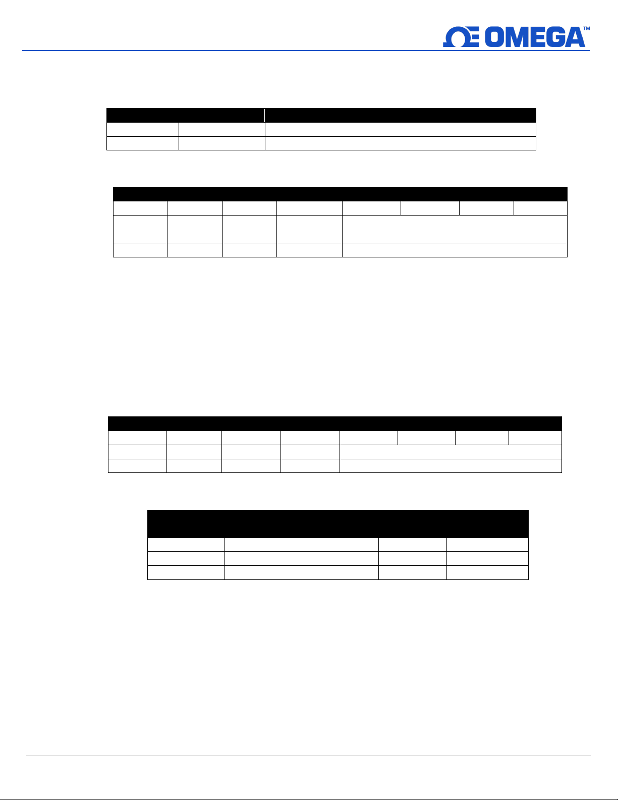
7.2.1.1 Process Measurement Types
Sensor Type
SI Derived Units
Measurement
0x11
mV
Process Voltage (0 - 1.0 V, 0 – 2.0 V)
0x13
mA
Process Current (0-24 mA current loop, common return)
Process Input Data Type/Format
7 6 5 4 3 2 1
0
Smart
Sensor
Factory
Calibrate
0 0 ?
0
0x06 = Float
Process Input Configuration
7 6 5 4 3 2 1
0
Available
Channel
Scaling
Lock
Sensor Range / Type
0
0* ? ?
(See Below)
Sensor
Range/Type
0x01
0-24 mA
0x13
Current (mA)
0x03
0-1.0 Vdc
0x11
Millivolts (mV)
0x09
0-2.0 Vdc
0x11
Millivolts (mV)
The Process interface provides a measurement dependent on the input range/type selected. The units of
measure may be changed by the user.
7.2.1.2 Process Input Data Type/Format
Writeable
7.2.1.2.1 Data Type
The 4-bit Data Type field determines the type of data of the specific sensor.
7.2.1.2.2 Factory Calibrate
Factory calibration is available for the process inputs. Clearing this bit will disable the factory
calibration values.
7.2.1.2.3 Writeable
The writeable bit is cleared, indicating that the sensor values may not be overwritten.
7.2.1.3 Process Input Configuration
7.2.1.3.1 Sensor Range / Type
Reserved Data Type
Sensor Input Type (Range) Measurement Type
7.2.1.3.2 Lock
If set, the user-specified units of measure string (4 character maximum) will be used in place of
the default units of measure.
7.2.1.3.3 Apply Scaling
If set, the user-defined Offset and Gain values will be used to adjust the sensor reading:
7.2.1.3.4 Assigned
The Assigned bit will always read as 0.
7.2.1.3.5 Available
The Available bit will always read as 0.
Result = (Raw Reading * Gain) + Offset
31 | M5751
Page 32
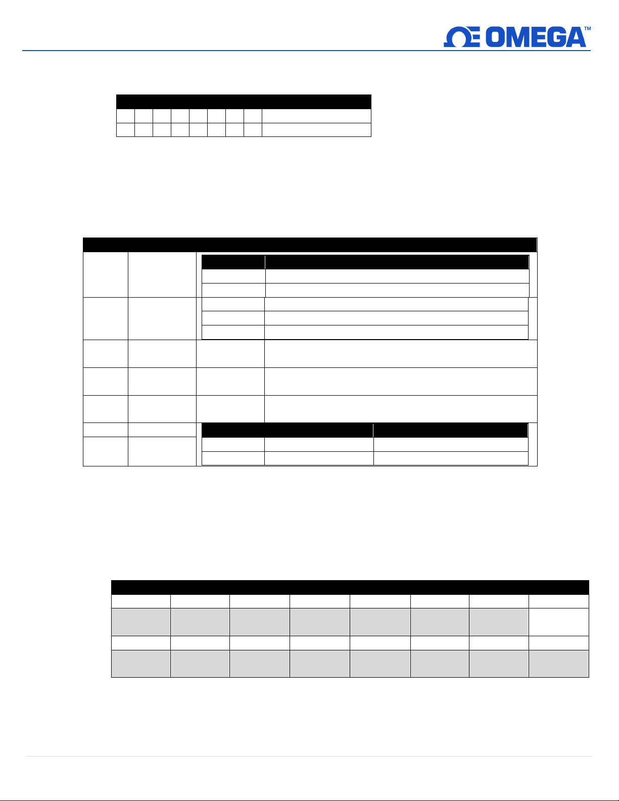
7.2.2 Process Device Byte
Analog Inputs
7 6 5 4 3 2 1 0 Description
1 X 0 0 0 0 0 0 Single Ended
Offset
Name
Value
Description
Value
Description
3317
Current (mA)
3316
Voltage (mV)
0-24 mA
1 - display as xx.x
0-1000 mV
-1 - display as xxx0.0
0-2000 mV
-1 - display as xxx0.0
Sensor
Trigger
Min
Measured
Max
Measured
0x08b8
Min Range
Range
Minimum
Maximum
0-24 mA0 24 mA
0 – 1 Vdc 0 1000 mV
Process Sensor Trigger Function
7 6 5 4 3 2 1
0
Reset
Min/Max
15
14
13
12
11
10 9 8
Calibration
Reset
Calibration
Status
Calibration
Mode
Capture
High
Capture
Low
Calibration
Start
The Sensor Device field determines the signal types for each of the channel bits.
7.2.3 Process Sensor Parameters
There are no Process Sensor Parameters.
7.2.4 Process IPSO Definition
The IPSO process definition provides signal range, measured min/max values, IPSO object type information.
0x08a8 Sensor Type
0x08aa Precision
0x08ac
0x08b0
0x08b4
?? Write any value to force a reset of min/max
?? Minimum reading since the last reset
?? Maximum reading since the last reset
0x08bc Max Range
7.2.4.1 Process Resolution
The measured mA value is rounded to provide +/- 0.1 mA resolution.
The measured mV value is rounded to provide +/- 10 mV resolution.
7.2.4.2 Process Sensor Trigger Function
The Sensor Trigger function is used to reset the IPSO min/max values as well as control the Calibration
process.
0 0 0 0 0 0 0
0 0
Setting the Reset Min/Max bit to 1 will reset the Min/Max values recorded by the IPSO process. No User
Calibration process is supported on the Process inputs and all configuration bits should be written as 0.
32 | M5751
Page 33
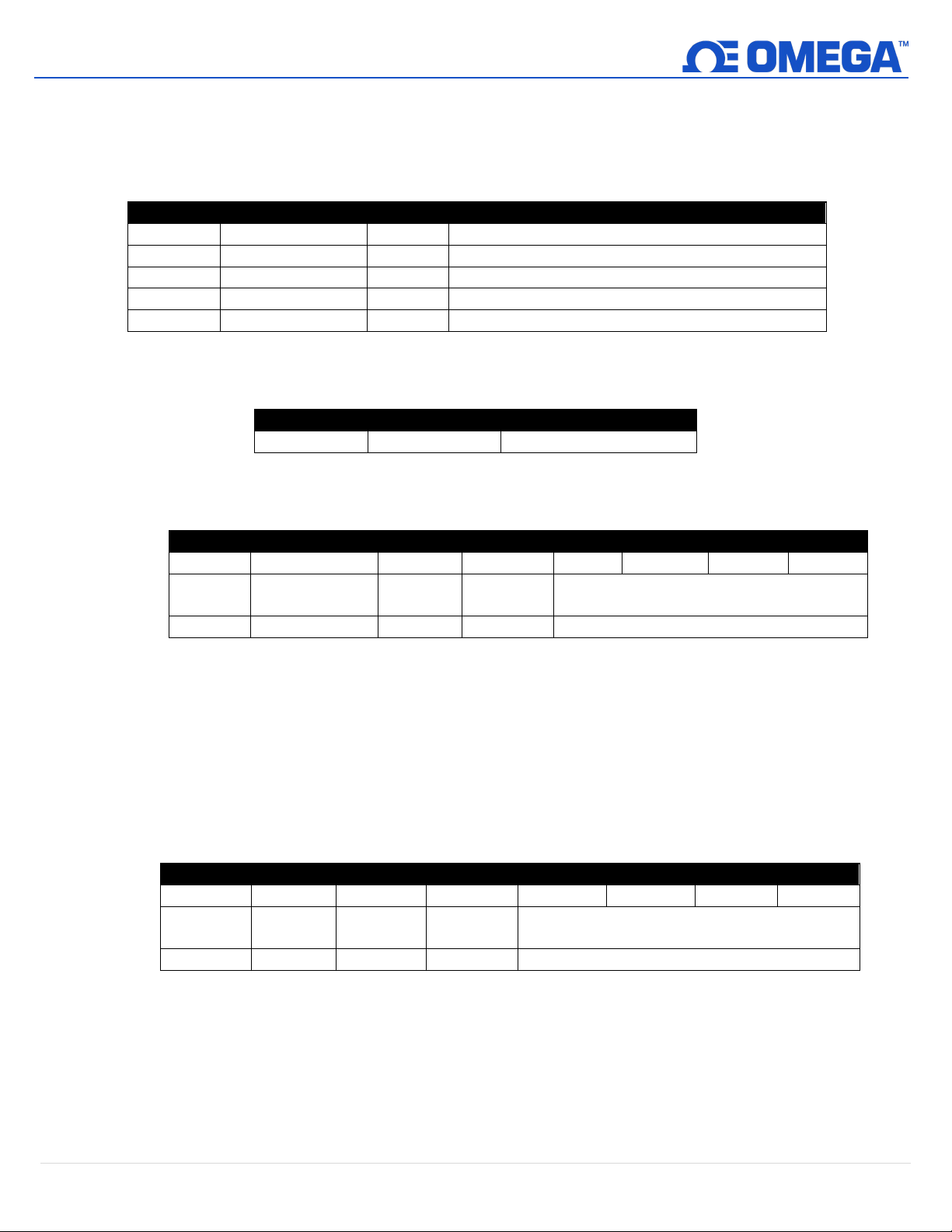
7.3 DIO Interface
Offset
Name
Value
Description
0x00
Sensor Type
0x18
Digital Type (Bit mapped)
0x01
Data Type/Format
0x46
Configurable, Float type
0x02
Configuration
0x23
Scaling applied, Bits 0 and 1 enabled
0x03
Sensor Device
0x0f
DIN bits enabled / inverted
0x04
UOMR
“DIN”
Units of measure
Sensor Type
SI Derived Units
Measurement
0x18
DIN
Bit mapped digital inputs
DIO Data Type/Format
7 6 5 4 3 2 1
0
Smart
Sensor
Sensor Value
Writeable
Factory
Calibrate
0 0 0
0
6 == Floating point
DIO Input Configuration
7 6 5 4 3 2 1
0
Assigned
Apply
Scaling
0 0 1
?
0x03 == bits 0 and 1
The DIO Interface provides 2 digital inputs which are hardwired to the Digital outputs. These may be used to detect
the state of external switches (output off) or to monitor the state of the outputs.
7.3.1 DIO Descriptor
7.3.1.1 DIO Sensor Type
The interface provides a bitmapped input of the 2 digital signal lines.
7.3.1.2 DIO Data Type/Format
7.3.1.2.1 Data Type
The 4-bit Data Type field determines the type of data of the specific sensor.
7.3.1.2.2 Factory Calibrate
The Factory Calibrate bit is not used for DIO types.
7.3.1.2.3 Sensor Value Writeable
This indicates that the sensor value may be overwritten. Not used on DIO inputs.
7.3.1.3 DIO Input Configuration
Available
7.3.1.3.1 Lock
If set, the user-specified units of measure string (4 character maximum) will be used in place of
the default DIN.
reserved Data Type
Lock Sub Channel Selection
7.3.1.3.2 Apply Scaling
If set, the user-defined Offset and Gain values will be used to adjust the sensor reading:
Result = (Raw Reading * Gain) + Offset
33 | M5751
Page 34
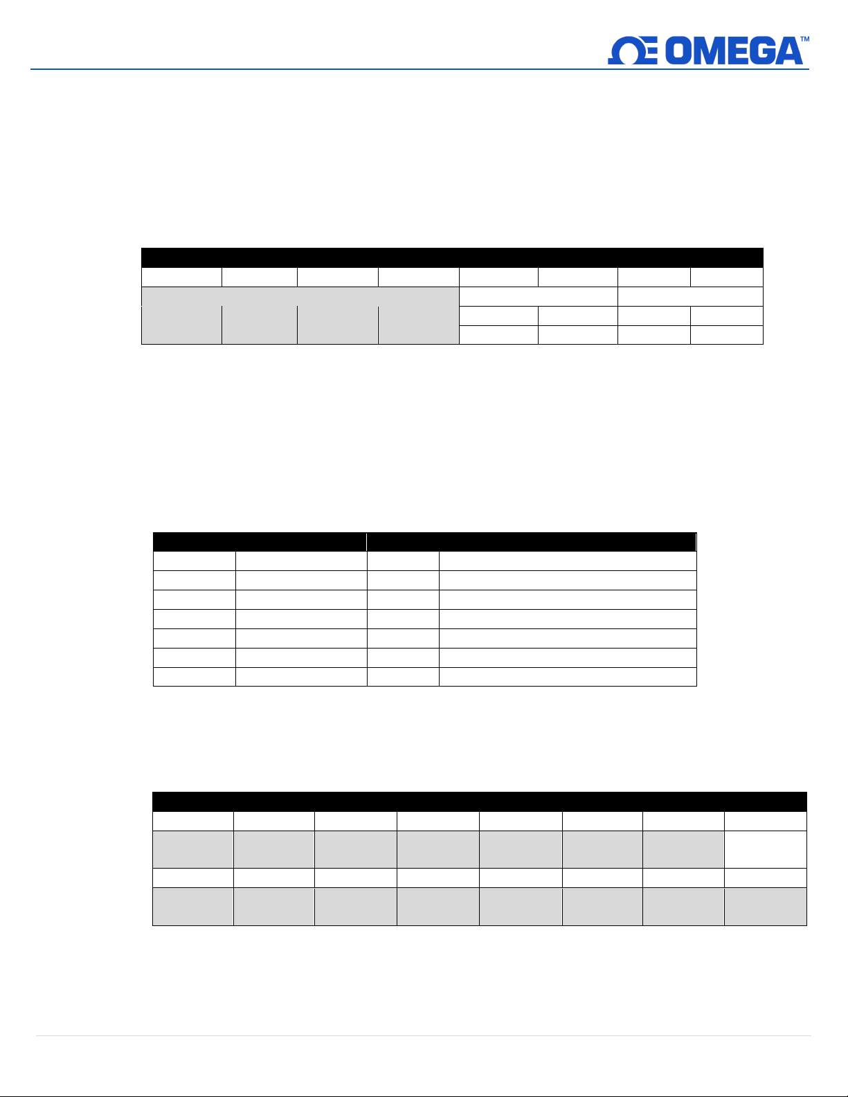
7.3.1.3.3 Assigned
DIO Device Configuration
7 6 5 4 3 2 1
0
Reserved
DIN 1
DIN 0
ENABLE
INVERT
ENABLE
INVERT
1 1 1
1
Offset
Name
Value
Description
0x08a8
Sensor Type
3349
Bit Mapped Digital
0x08aa
Precision
0
Provides reading of xxx
0x08ac
Reset Min/Max
??
Write 0x0001 force reset of min / max
0x08b0
Min Measured
??
Minimum reading since the last reset
0x08b4
Max Measured
??
Maximum reading since the last reset
0x08b8
Min Range
0
Minimum reading
0x08bc
Max Range
3
Maximum reading
Sensor Trigger Function
7 6 5 4 3 2 1
0
Reset
Min/Max
15
14
13
12
11
10 9 8
Calibration
Reset
Calibration
Status
Calibration
Mode
Capture
High
Capture
Low
Calibration
Start
The Assigned bit will always read as 0.
7.3.1.3.4 Available
The Available bit will always read as 0.
7.3.1.4 DIO Device Configuration
The DIO Device Configuration allows enabling each of the 2 input bits and selecting whether the input is
active HIGH (reads as 1 when input is not grounded) or active LOW (reads as 1 when input is grounded).
0 0 0 0
7.3.1.4.1 Invert
If the Invert bit is set the input is active LOW.
7.3.1.4.2 Enable
If the Enable bit is set the input is enabled.
7.3.1.5 DIO IPSO Definition
The DIO input IPSO definition provides signal range, measured min/max values, IPSO object type
information.
7.3.1.6 Sensor Trigger Function
The Sensor Trigger function is used to reset the IPSO min/max values as well as control the calibration
process.
0 0 0 0 0 0 0
0 0
Setting the Reset Min/Max bit to 1 will reset the Min/Max values recorded by the IPSO process. No User
Calibration process is supported on the DIO inputs and all bits should be written as 0.
34 | M5751
Page 35
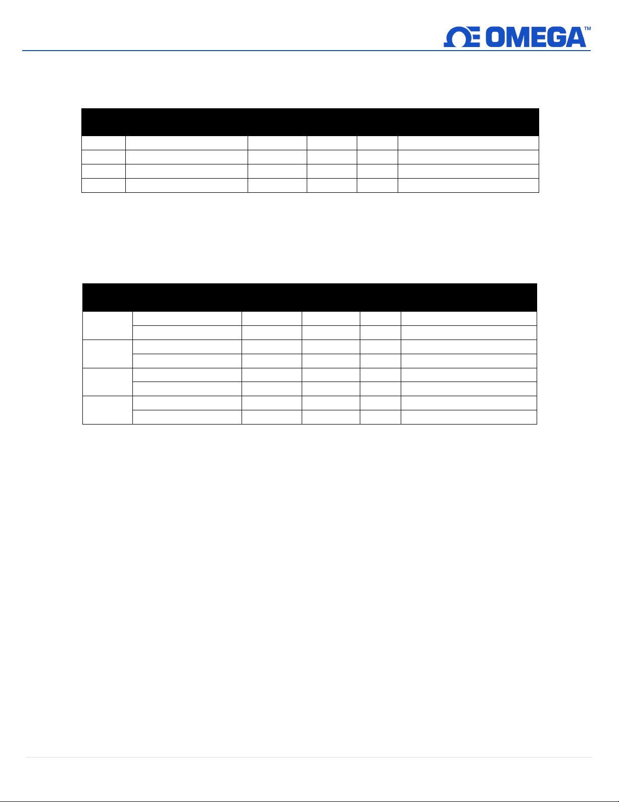
7.4 Output Interface
Modbus
Address
I2C
Address
0
Output 0 Descriptor
0xf09a
0x0134
uint16
PWM 0 (see below)
1
Output 1 Descriptor
0xf09b
0x0136
uint16
PWM 1 (see below)
2
Output 2 Descriptor
0xf09c
0x0138
uint16
Phantom (non-configurable)
3
Output 3 Descriptor
0xf09d
0x013a
uint16
Phantom (non-configurable)
Modbus
Address
I2C
Address
Output 0 Low Scale
0xf1f0
0x03e0
float
Sets lower input range
Output 0 High Scale
0xf1f2
0x03e4
float
Sets upper input range
Output 1 Low Scale
0xf1f4
0x03e8
float
Sets lower input range
Output 1 High Scale
0xf1f6
0x03ec
float
Sets upper input range
Output 2 Low Scale
0xf1f8
0x03f0
float
Sets lower input range
Output 2 High Scale
0xf1fa
0x03f4
float
Sets upper input range
Output 3 Low Scale
0xf1fc
0x03f8
float
Sets lower input range
Output 3 High Scale
0xf1f2e
0x03fc
float
Sets upper input range
Outputs share a common structure which consists of 3 fields mapped to a 16-bit unsigned integer, accessible in the
Smart Sensor register map.
Output Name
Refer to the specific output type for further information.
7.4.1 Scaling Minimum / Maximum Values
When Input Mapping is used the user may specify the input signal range through the Input Minimum and
Input Maximum parameters. There is one pair of registers for each of the 4 possible outputs.
Sensor Name
0
1
2
3
Size Typical Description
Size Description
When either the Low Scale or High Scale value changes, an internal calculation is performed to calculate the
linear transformation to be applied to the sensor reading.
35 | M5751
Page 36
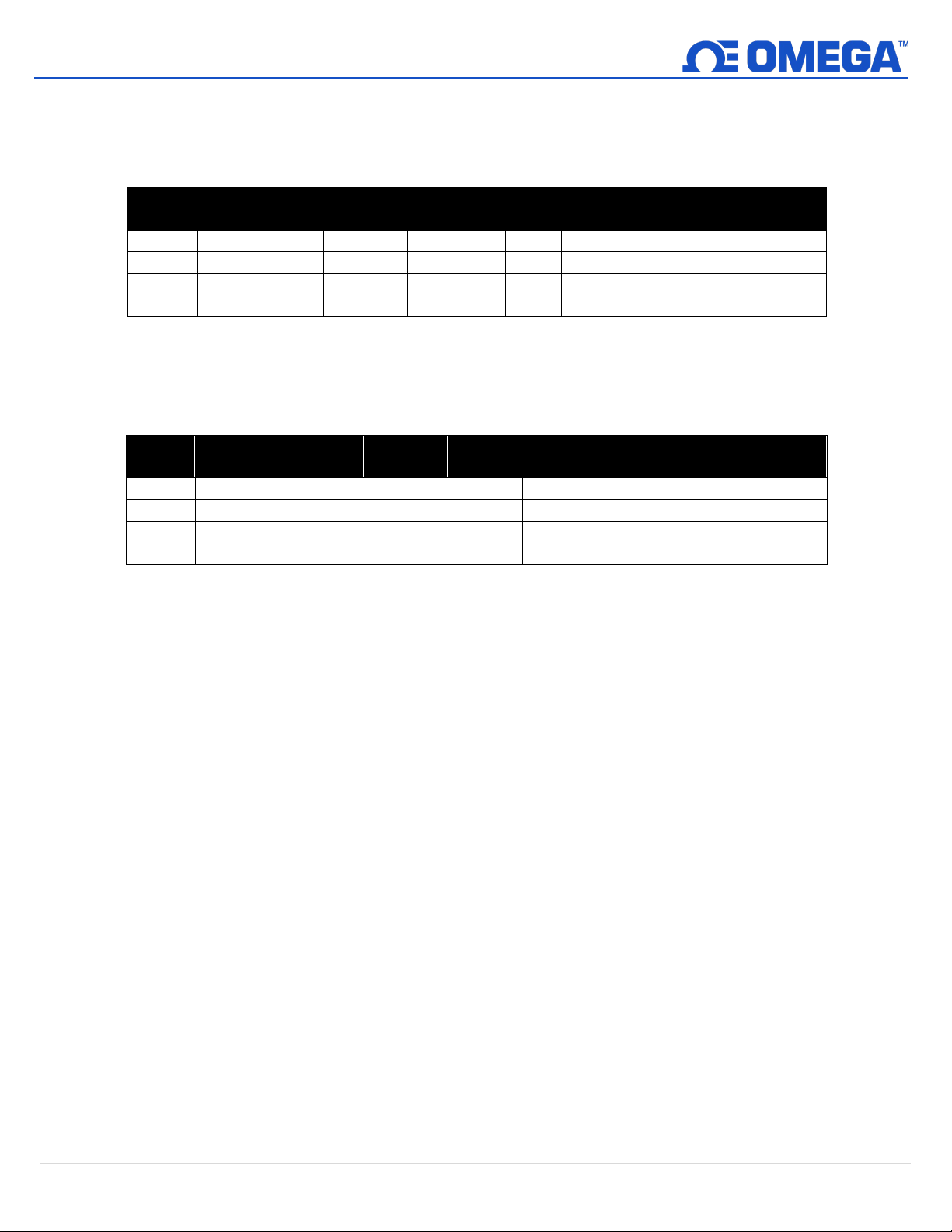
7.4.2 Output Values
Modbus
Address
I2C
Address
0
Output 0 Value
0xf078
0x00f0
float
Percent of full-scale value (0-100%)
1
Output 1 Value
0xf07a
0x00f4
float
Percent of full-scale value (0-100%)
2
Output 2 Value
0xf07c
0x00f8
float
Percent of full-scale value (0-100%)
3
Output 3 Value
0xf07e
0x00fc
float
Percent of full-scale value (0-100%)
Modbus
Address
I2C
Address
0
Output 0 Name
0xf720
0x0e40
char[16]
Defaults to Output_0
1
Output 1 Name
0xf728
0x0e50
char[16]
Defaults to Output_1
2
Output 2 Name
0xf730
0x0e60
char[16]
Defaults to Output_2
3
Output 3 Name
0xf738
0x0e70
char[16]
Defaults to Output_3
Outputs use float values which represent the percentage of full scale. If the output is not mapped, the value
written (0 – 100%) is identical to the value that is read back. If the output is mapped, the scaling values are
used to transform the minimum input value to 0% and the maximum input value to 100%.
Output Name
7.4.3 Output Names
Each output has a name. The default names for the outputs are Output_0 through Output_3. The default
names may be overwritten, such as ‘Stack_Lite’ or ‘Control_Valve’. Names are restricted to 16 characters.
Output Name
The Output names are retained until a factory reset occurs. It is strongly recommended that:
1) Spaces within the name should be replaced with the ‘_’ character.
Size Description
Size Description
2) All output names on a particular device are unique – if duplicate functions are supported append a ‘_x’
string, where x represents the instance. For example, Stack_Lite_1 and Stack_Lite_2 could be used if 2
stack lights are being connected.
36 | M5751
Page 37
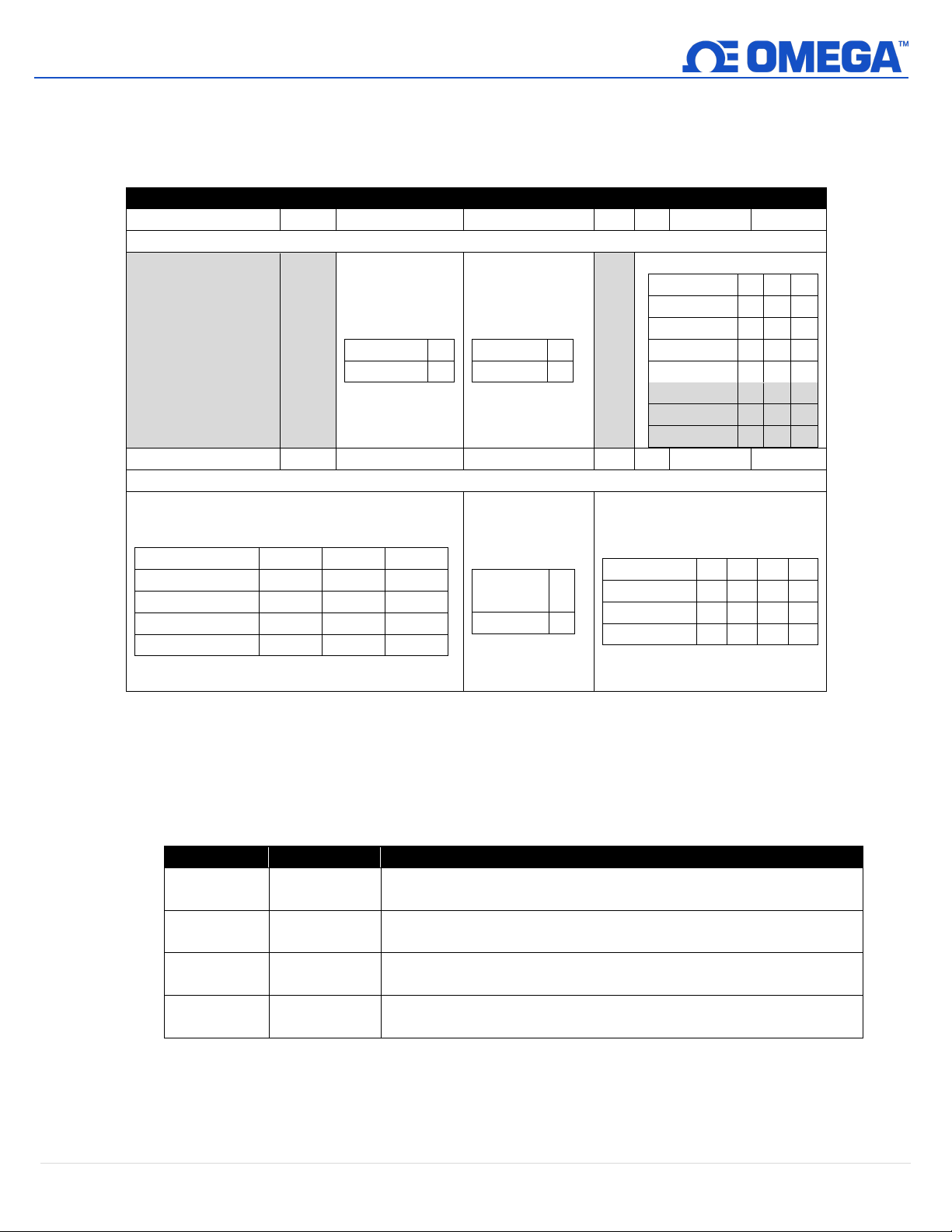
7.5 Digital Output Configuration
Digital Output Configuration
7 6 5
4
3 2 1
0
Output Configuration
1.0 – 2.0
0
0.5 – 2.5
1
LOW
0
HIGH
1
Rate
100 Hz
0 0 0
10 Hz
0 0 1
1 Hz
0 1 0
0.1 Hz
0 1 1
50 Hz
1 0 0
33 Hz
1 0 1
25 Hz
1 1 0
20 Hz
1 1 1
15
14
13
12
11
10 9 8
Output Type
No Mapping
0 - -
Sensor 0
1 0 0
Sensor 1
1 0 1
Sensor 2
1 1 0
Sensor 3
1 1 1
Not
Enabled
0
Enabled
1
Null
0 0 0
0
ON/OFF
0 0 0
1
PWM
0 0 1 0 Servo
0 0 1
1
PWM Rate
Name
Description
PWM signal has constant 100 Hertz frequency (10 msec repetition
rate) with 0 – 100 % duty cycle
PWM signal has constant 10 Hertz frequency (100 msec repetition
rate) with 0 – 100 % duty cycle
PWM signal has constant 1 Hertz frequency (1-second repetition
rate) with 0 – 100 % duty cycle
PWM signal has constant 0.1 Hertz frequency (10-second
repetition rate) with 0 – 100 % duty cycle
Two output signals are available which may be configured for ON/OFF, PWM, or SERVO outputs through the Output
Configuration registers (0x0124 and 0x0126). The remaining outputs are assigned as phantom devices which are
non-configurable. The highlighted entries show typical default configurations.
7.5.1 Rate
The Rate determines the repetition rate, or frequency, of the Digital Output. For On/Off outputs the rate
field is ignored.
Sensor Mapping
Servo Range
Active State
Mapping Enable
Output Type
7.5.1.1 PWM Rate
The SP-013 supports the following PWM frequencies:
0 100 Hz
1 10 Hz
2 1 Hz
3 0.1 Hz
37 | M5751
Page 38
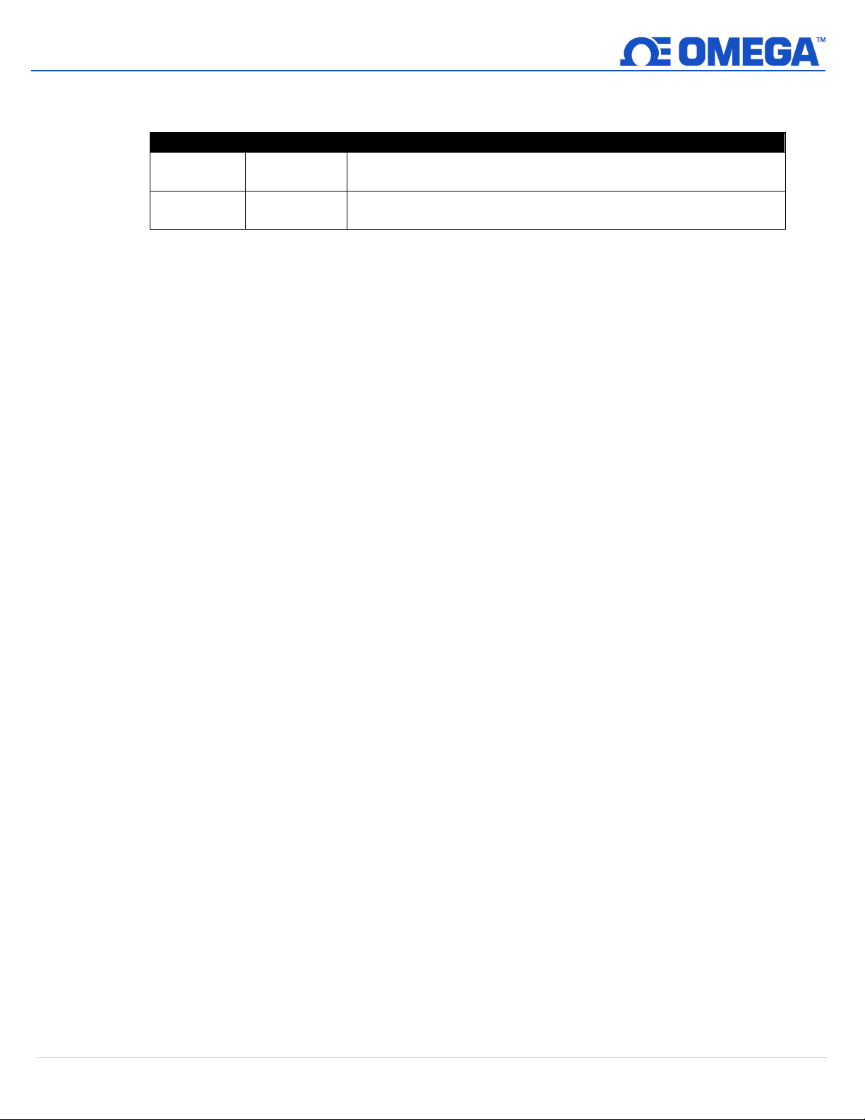
7.5.1.2 SERVO Rate
PWM Rate
Name
Description
PWM signal has a constant 100 Hertz frequency (10 msec
repetition rate)
PWM signal has a constant 50 Hertz frequency (20 msec repetition
rate)
Smart Sensor probes support the following SERVO frequencies:
0 100 Hz
4 50 Hz
7.5.2 Output Type
Smart Sensor probes support NULL (0), ON/OFF (1), PWM (2), and SERVO (3) outputs. When set to NULL the
output signal will be left in a high impedance state. When set to ON/OFF the Rate and Servo Range controls
have no effect. When the SERVO type is selected the Duty-Cycle is restricted so the output signal is either
0.5 – 2.5 msec or 1.0 to 2.0 msec based on the Servo Range bit.
7.5.3 Active State
Smart Sensor digital outputs may be configured as Active HIGH or Active LOW. When set to 1 (Active High),
the output will be high impedance when active. When set to 0 (Active Low), the output will be low
impedance (~ 0.0 volts) when active. The Factory reset value is 0 (Low).
7.5.4 Mapping Enabled
The read-only Mapping Enabled bit indicates that the output may be optionally directly mapped to a sensor
input based on the Sensor Mapping field. If the Mapping Enabled bit is clear no mapping is supported, and
the Sensor Mapping field is ignored.
7.5.5 Sensor Mapping
The Sensor Mapping value may select ‘no mapping’ or of any Sensor. If no mapping is selected the output
may be directly controlled by writing a value from 0 – 100 % to the internal Output Value. If a Sensor is
selected and the hardware supports the mapping the output will track the selected sensor value, scaled by
the Input Minimum and Input Maximum values.
If Sensor Mapping is enabled for PWM outputs the scaling values are used such that a signal input at or
below the Scaling Low-value results in a 0% output and a signal input at or above the Scaling High-value
results in a 100% PWM duty cycle.
If Sensor Mapping is enabled for SERVO outputs the scaling values are used such that a signal input at or
below the Scaling Low-value results in a minimum (0.5 or 1.0 msec) pulse width and a signal input at or
above the Scaling High-value results in a maximum (2.0 or 2.5 msec) pulse width.
38 | M5751
Page 39

WARRANTY/DISCLAIMER
OMEGA ENGINEERING, INC. warrants this unit to be free of defects in materials and workmanship for a
period of 13 months from date of purchase. OMEGA’s WARRANTY adds an additional one (1) month
grace period to the normal one (1) year product warranty to cover handling and shipping time. This
ensures that OMEGA’s customers receive maximum coverage on each product.
If the unit malfunctions, it must be returned to the factory for evaluation. OMEGA’s Customer Service
Department will issue an Authorized Return (AR) number immediately upon phone or written request.
Upon examination by OMEGA, if the unit is found to be defective, it will be repaired or replaced at no
charge. OMEGA’s WARRANTY does not apply to defects resulting from any action of the purchaser,
including but not limited to mishandling, improper interfacing, operation outside of design limits,
improper repair, or unauthorized modification. This WARRANTY is VOID if the unit shows evidence of
having been tampered with or shows evidence of having been damaged as a result of excessive corrosion;
or current, heat, moisture or vibration; improper specification; misapplication; misuse or other operating
conditions outside of OMEGA’s control. Components in which wear is not warranted, include but are not
limited to contact points, fuses, and triacs.
OMEGA is pleased to offer suggestions on the use of its various products. However,
OMEGA neither assumes responsibility for any omissions or errors nor assumes liability for
any damages that result from the use of its products in accordance with information provided
by OMEGA, either verbal or written. OMEGA warrants only that the parts manufactured by the
company will be as specified and free of defects. OMEGA MAKES NO OTHER WARRANTIES OR
REPRESENTATIONS OF ANY KIND WHATSOEVER, EXPRESSED OR IMPLIED, EXCEPT THAT OF
TITLE, AND ALL IMPLIED WARRANTIES INCLUDING ANY WARRANTY OF MERCHANTABILITY
AND FITNESS FOR A PARTICULAR PURPOSE ARE HEREBY DISCLAIMED. LIMITATION OF
LIABILITY: The remedies of purchaser set forth herein are exclusive, and the total liability of
OMEGA with respect to this order, whether based on contract, warranty, negligence,
indemnification, strict liability or otherwise, shall not exceed the purchase price of the
component upon which liability is based. In no event shall OMEGA be liable for
consequential, incidental or special damages.
CONDITIONS: Equipment sold by OMEGA is not intended to be used, nor shall it be used: (1) as a “Basic
Component” under 10 CFR 21 (NRC), used in or with any nuclear installation or activity; or (2) in medical
applications or used on humans. Should any Product(s) be used in or with any nuclear installation or
activity, medical application, used on humans, or misused in any way, OMEGA assumes no responsibility
as set forth in our basic WARRANTY/ DISCLAIMER language, and, additionally, purchaser will indemnify
OMEGA and hold OMEGA harmless from any liability or damage whatsoever arising out of the use of the
Product(s) in such a manner.
RETURN REQUESTS/INQUIRIES
Direct all warranty and repair requests/inquiries to the OMEGA Customer Service Department.
BEFORE RETURNING ANY PRODUCT(S) TO OMEGA, PURCHASER MUST OBTAIN AN AUTHORIZED
RETURN (AR) NUMBER FROM OMEGA’S CUSTOMER SERVICE DEPARTMENT (IN ORDER TO AVOID
PROCESSING DELAYS). The assigned AR number should then be marked on the outside of the return
package and on any correspondence.
The purchaser is responsible for shipping charges, freight, insurance and proper packaging to prevent
breakage in transit.
FOR WARRANTY RETURNS, please have the
following information available BEFORE contacting
OMEGA:
1. Purchase Order number under which the product
was PURCHASED,
2. Model and serial number of the product under
warranty, and
3. Repair instructions and/or specific problems
relative to the product.
OMEGA’s policy is to make running changes, not model changes, whenever an improvement is possible. This affords
our customers the latest in technology and engineering.
OMEGA is a trademark of OMEGA ENGINEERING, INC.
© Copyright 2019 OMEGA ENGINEERING, INC. All rights reserved. This document may not be copied, photocopied,
reproduced, translated, or reduced to any electronic medium or machine-readable form, in whole or in part, without the
prior written consent of OMEGA ENGINEERING, INC.
FOR NON-WARRANTY REPAIRS,
OMEGA for current repair charges. Have
the following information available BEFORE
contacting OMEGA:
1. Purchase Order number to cover the COST
of the repair,
2. Model and serial number of the product, and
3. Repair instructions and/or specific problems
relative to the product.
consult
Page 40

Where Do I Find Everything I Need for
Process Measurement and Control?
OMEGA…Of Course!
Shop online at omega.com
TEMPERATURE
MU
Thermocouple, RTD & Thermistor Probes, Connectors, Panels & Assemblies
MU
Wire: Thermocouple, RTD & Thermistor
MU
Calibrators & Ice Point References
MU
Recorders, Controllers & Process Monitors
MU
Infrared Pyrometers
PRESSURE, STRAIN AND FORCE
MU
Transducers & Strain Gages
MU
Load Cells & Pressure Gages
MU
Displacement Transducers
MU
Instrumentation & Accessories
FLOW/LEVEL
MU
Rotameters, Gas Mass Flowmeters & Flow Computers
MU
Air Velocity Indicators
MU
Turbine/Paddlewheel Systems
MU
Totalizers & Batch Controllers
pH/CONDUCTIVITY
MU
pH Electrodes, Testers & Accessories
MU
Benchtop/Laboratory Meters
MU
Controllers, Calibrators, Simulators & Pumps
MU
Industrial pH & Conductivity Equipment
DATA ACQUISITION
MU Communications-Based Acquisition Systems
MU Data Logging Systems
MU Wireless Sensors, Transmitters, & Receivers
MU Signal Conditioners
MU Data Acquisition Software
HEATERS
MU
Heating Cable
MU
Cartridge & Strip Heaters
MU
Immersion & Band Heaters
MU
Flexible Heaters
MU
Laboratory Heaters
ENVIRONMENTAL
MONITORING AND CONTROL
MU
Metering & Control Instrumentation
MU
Refractometers
MU
Pumps & Tubing
MU
Air, Soil & Water Monitors
MU
Industrial Water & Wastewater Treatment
MU
pH, Conductivity & Dissolved Oxygen Instruments
M5751/1022
 Loading...