

Page 1

Service Manual
For LCD TV
(2004.2)
Page 2

Table of Contents
…
.
…
1 Introduction……..…………..……………………………………… P3
1.0 Preface……………………………………………………………………………P3
1.1 Caution……………………………………...……………………………………P3
1.2 Warning…………………………………………………………………………. P3
2 System Block Diagram……………………………………………..
2.0 System Block Diagram (ME)…………………………………………………
2.1 System Block Diagram (EE)……………………………………………………
2.2 Connector Connection Diagram……………………………………………….
2.3 Spare Parts List…………………………………………………………………
2.3.1 EE parts list……………………………………………………………………...
2.3.2 ME parts list……………………………………………………………………..
2.4 Connector Pin Definition……………………………………………………….
3 Schematic……………………………………………………………
3.0 Tuner Board……………..………………………………………………………
3.1 Graph Port Tuner……………………………………………………………….
3.2 Interface Board…………..……………………………………………………
3.3 IR Board……..…………..………………………………………………………
3.4 Keypad Board…….……..………………………………………………………
3.5 System Board-1 Graph Interface………………………………………………
3.6 System Board-2 Power Management….………………………………………
P5
P5
P6
P7
P8
P8
P14
P24
P40
P40
P41
P42
P43
P44
P45
P46
3.7 System Board-3 PW181 Power Management….………………………………
3.8 System Board-4 DVI Receiver………………….………………………………
3.9 System Board-5 ADC………………………..….………………………………
3.10 System Board-6 A/V Switch…………………….………………………………
3.11 System Board-7 3D Comb Filter…………….….………………………………
3.12 System Board-8 Video Decoder (V Port)……….………………………………
3.13 System Board-9 Video Decoder (G Port)……….………………………………
3.14 System Board-10 Deinterlace…………………...………………………………
3.15 System Board-11 SDRAM……………………….………………………………
3.16 System Board-12 Image Processor………….….………………………………
3.17 System Board-13 Flash Memory…………….….………………………………
3.18 System Board-14 Miscellaneous………………...………………………………
3.19 System Board-15 LVDS………………………….………………………………
3.20 System Board-16 Audio DSP…………………….………………………………
3.21 System Board-17 Class D Audio PA…………….………………………………
1
P47
P48
P49
P50
P51
P52
P53
P54
P55
P56
P57
P58
P59
P60
P61
Page 3

4 TroubleShooting…………………………………………………….
P62
5 Firmware upgrade applications……………………………………
6 Standard Operation Procedure……………………………………
6.0 Module assembly process………………………………………………………
6.1 Module repair process………………………………………………………….
6.1.1 Tuner & Interface module……………………………………………………...
6.1.2 Stand module……………………………..……………………………………..
6.1.3 Back Cover & Speaker module……………………………..……...…………..
6.1.4 PCBA module………………………………………………..……...…………..
6.1.5 Power module………………………………………………..……...…………..
6.1.6 LCD module………………………...………………………..……...…………..
P68
P69
P69
P72
P72
P73
P74
P75
P76
P77
2
Page 4

1. Introduction
1.0 Preface
This service manual aims directly at the module of LCD TV. It offers the simple
repair which emphasizes on technique explanation and production troubles to
remove for the engineers and technicians who have electronic background.
1.1 Caution
Be sure to read those manual before servicing. To assure safety from fire, electric
shock, injury, harmful radiation and materials, various measures are provided in
this Prokia LCD TV. Be sure to read cautionary items described in the manual to
maintain safety before servicing.
1.2 Warning
1. Remember to unplug the AC cord from the AC outlet before cleaning the
product. And do not use liquid cleaners or aerosol cleaners to clean the
display.
2. Do not place the product on an unstable place. It can cause the product to fall,
resulting in serious personal injuries as well as damage to the product.
3. In case the product needs replacement parts, make sure that the service
person uses replacement parts specified by the manufacturer, or those with
the same characteristics and performance as the original parts. Use of
unauthorized parts can result in fire, electric shock and/or other danger.
4. Do not overload AC outlets or extension cords. It can cause fire or electric
shock.
5. The AC cords must be routed properly to prevent people from stepping on
them or objects from resting on them. Check the cords at the plugs and
product.
6. Do not hit the panel. Be careful to prevent from getting hurt by broken glass
pieces in case the panel breaks.
7. Keep the product away from heat sources such as radiators, heaters, stoves
and other heat-generating products.
8. Do not place the display near water. Like bathtub, washbasin, kitchen sink
and laundry tub, swimming pool and in a wet basement.
3
Page 5

Page 6
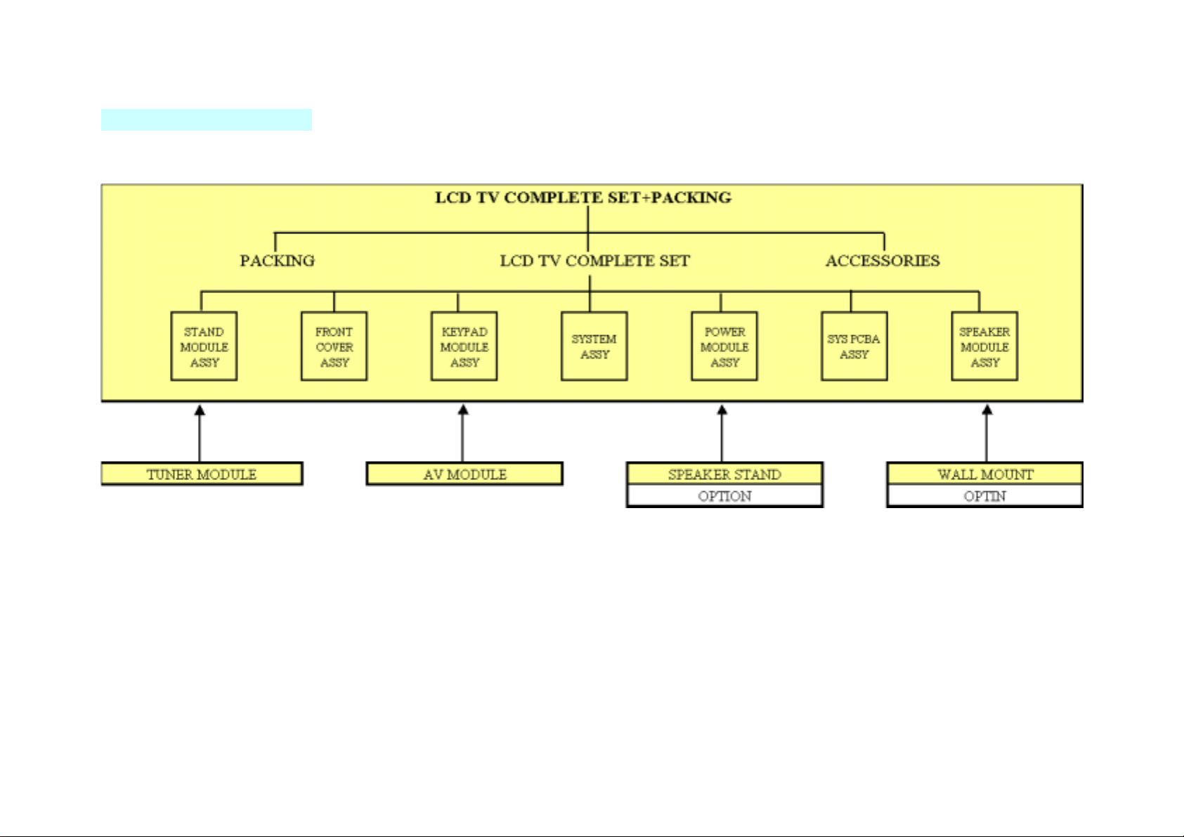
2. System Block Diagram
2.0 System Block Diagram (ME)
5
Page 7
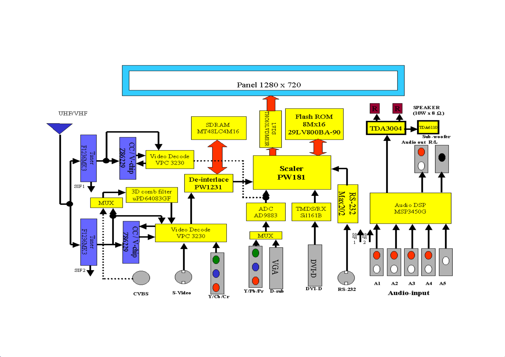
2.1 System Block Diagram (EE)
6
Page 8
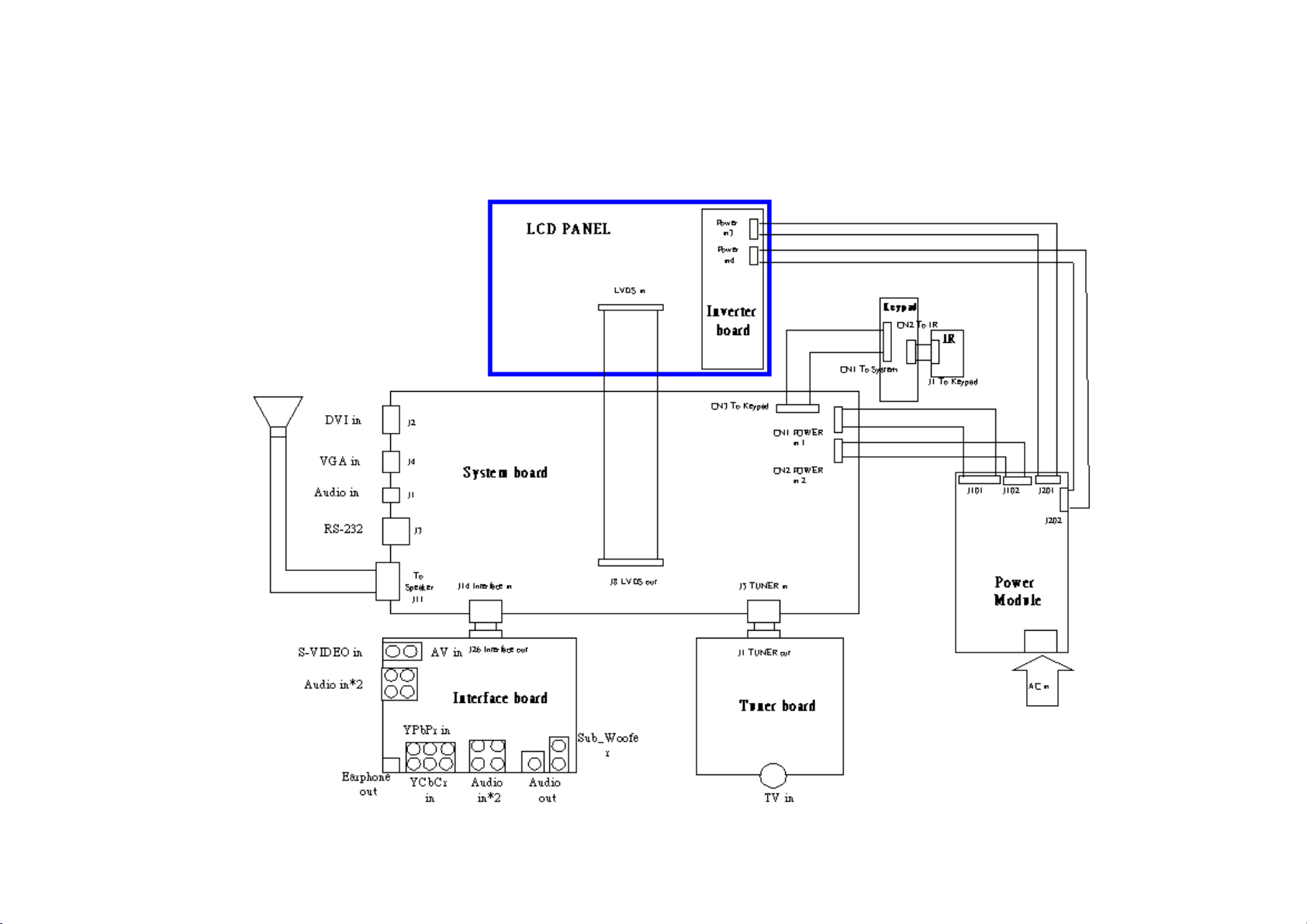
2.2 Connector Connection Diagram
7
Page 9
2.3 Spare Parts List
2.3.1 EE parts list
1. System Board for 27inch & 30inch
P/N: P061P3112011 for 27〞 P061P3112010 for 30〞
2. P311 Interface Module Assy
P/N: P70403820000
8
Page 10
3. P311 Tuner Module Assy
P/N: P70403830000
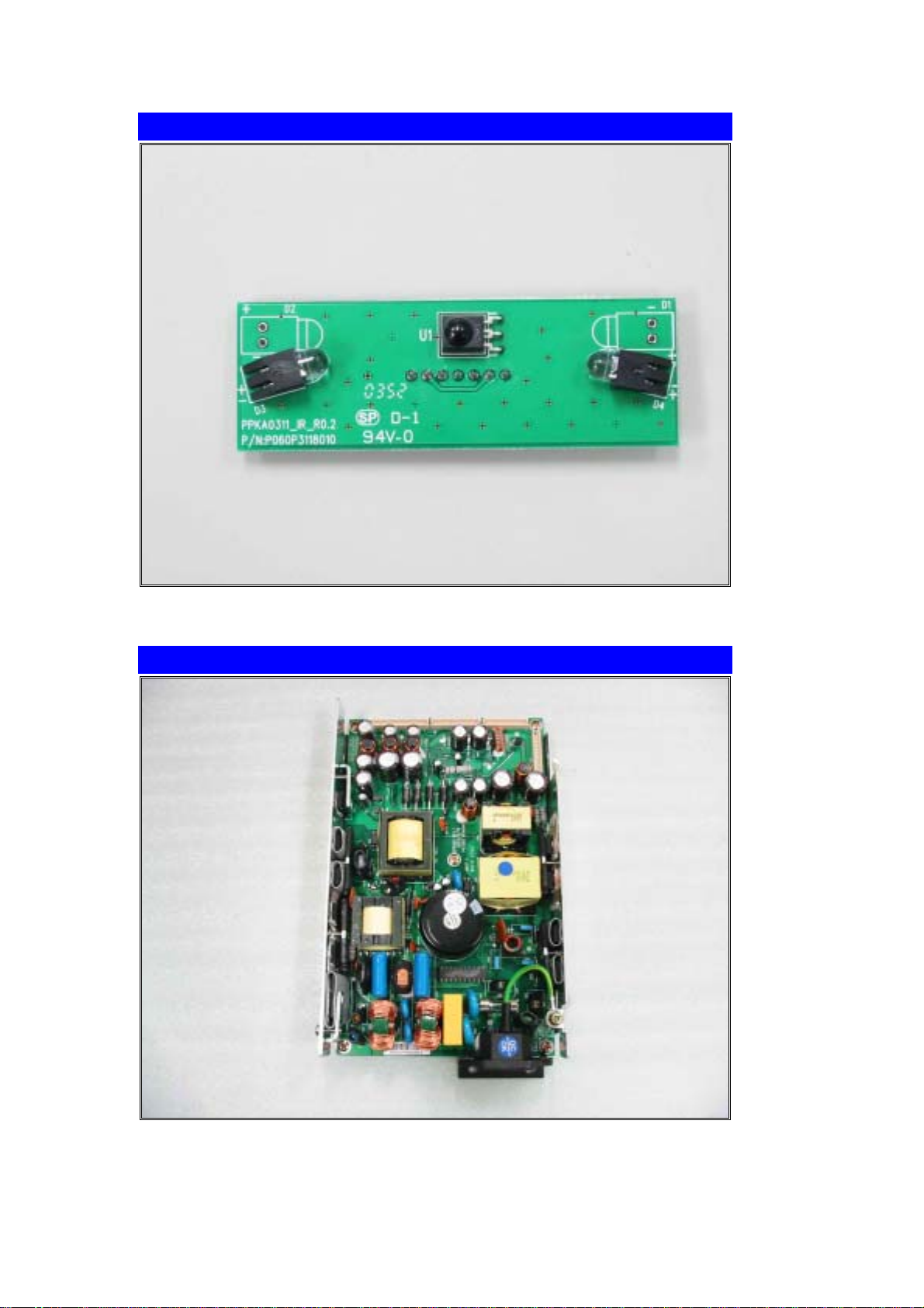
4. PCBA Keypad
P/N: P061P3117010
9
Page 11
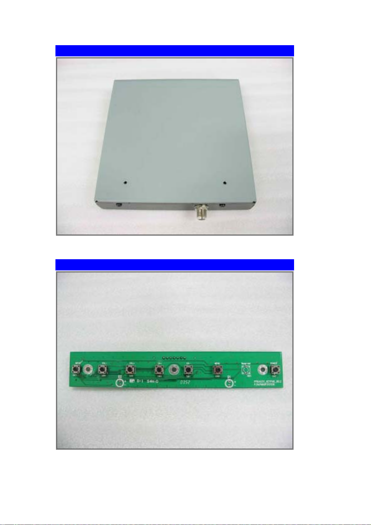
5. IR board
P/N: P061P3118010
6. Power Supply
P/N: P16000100000
10
Page 12
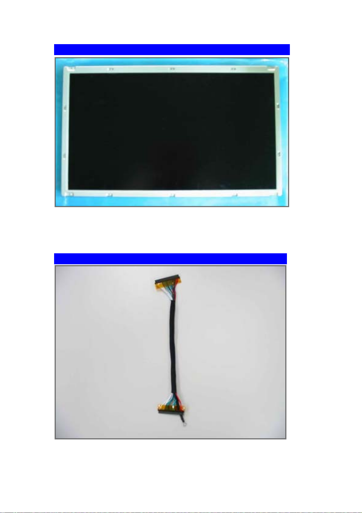
7. LCD Panel
P/N: P49000620000 for 27〞 P49000610000 for 30〞
8. System to Panel
P/N: P10W53000001
11
Page 13
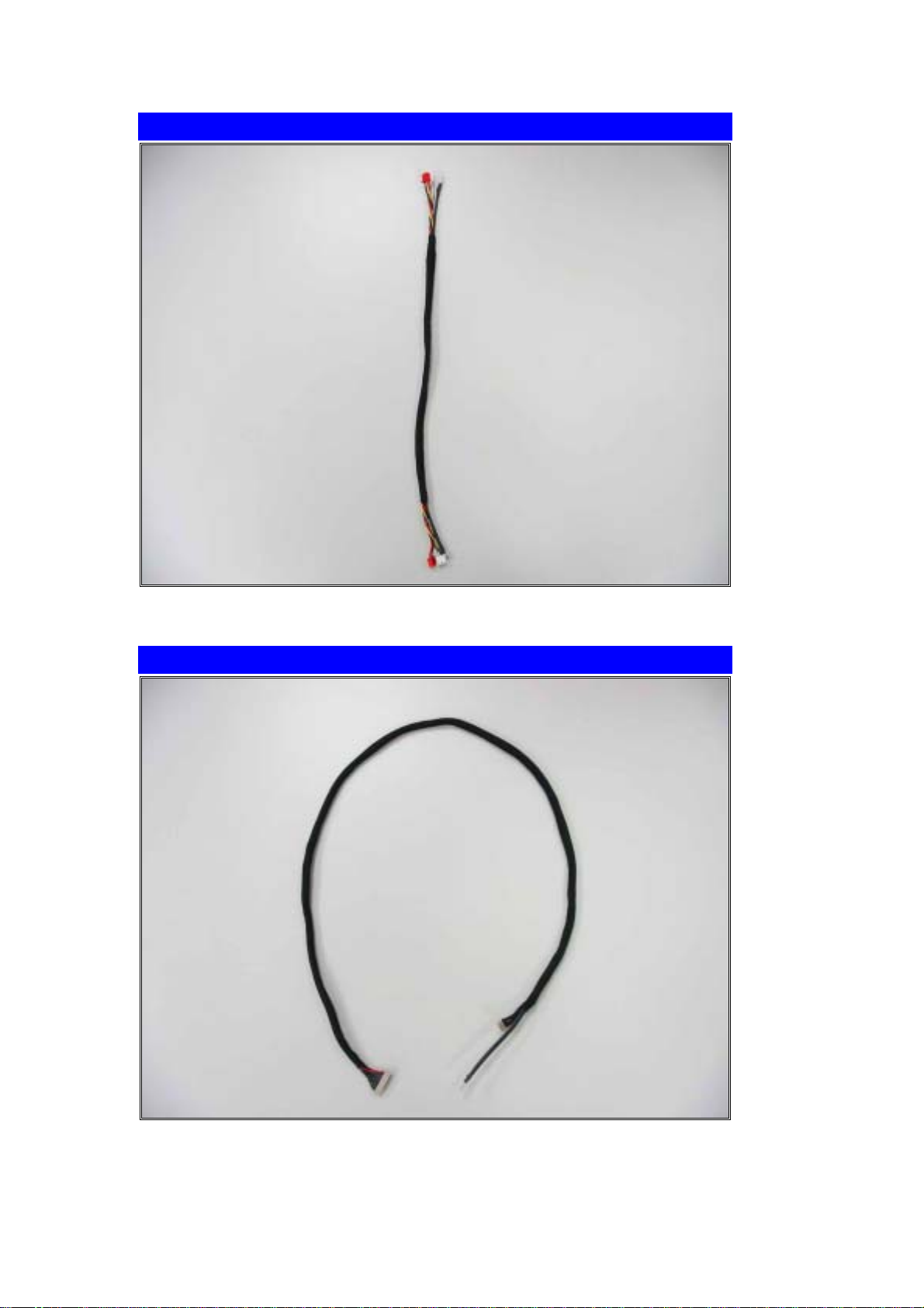
9. System to Speaker
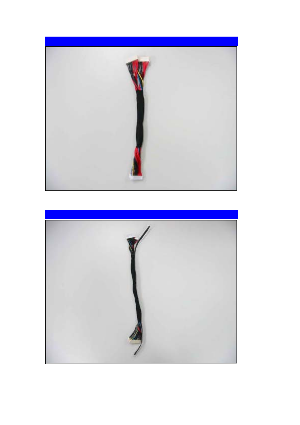
P/N: P10W50600001
10. System to Keypad
P/N: P10W51500002
12
Page 14
11. Power to Inverter
P/N: P10W62200001
12. System to Power
P/N: P10W62600001
13
Page 15
2.3.2 ME parts list
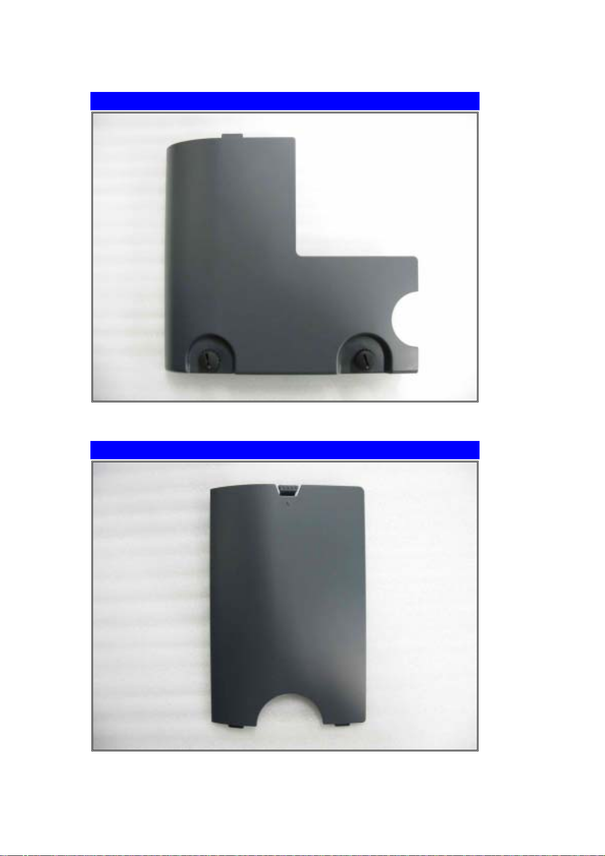
1. AV Cover Module Assy
P/N: P76000800000
2. Interface Cover
P/N: P60002040000
14
Page 16
3. Conn fix Cover Module Assy
P/N: P76000800000
4. Foot Base Bottom
P/N: P60001981000
15
Page 17
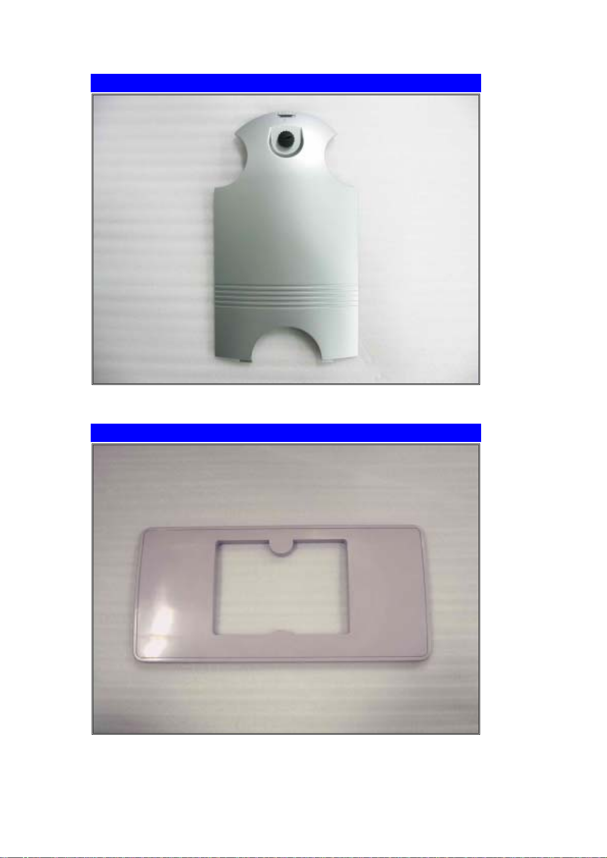
5. Foot Base Up
P/N: P60001980000
6. Al V ertical Support
P/N: P21001320000
16
Page 18
7. Foot Base Metal
P/N: P21001300000
8. Plastic Foot (GL-6)
P/N: P60001880000
17
Page 19
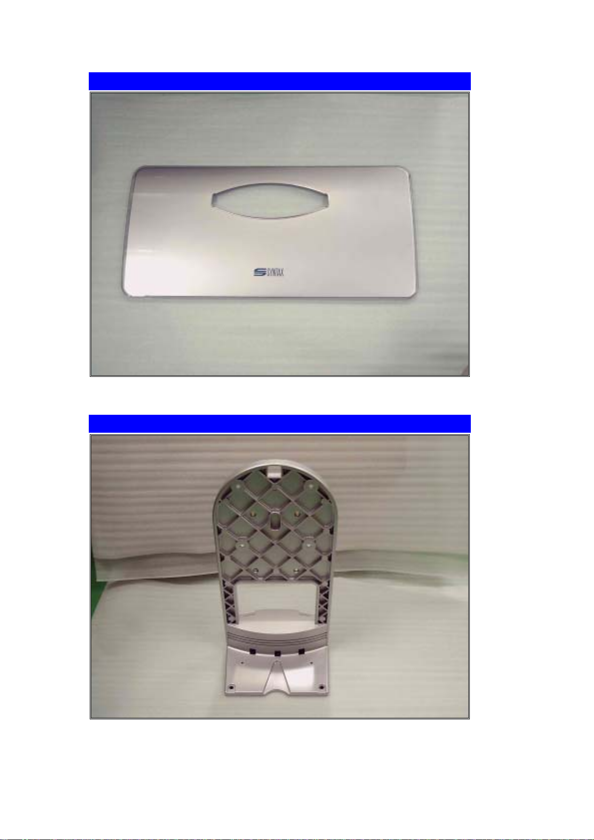
9. Keypad Assembly LCD TV
P/N: P76000790000
10. Speaker Module Assy
P/N: P76000750000
18
Page 20
11. Speaker Foot Module Assy
P/N: P76000760000
12. Power Shielding Up
P/N: P21001360000
19
Page 21
13. PCB-Support
P/N: P21001390000
14. PCB Support Metal
P/N: P21001380000 for 27〞 P21001390000 for 30〞
20
Page 22
15. System PCB Shielding
P/N: P21001370000
16. Back Cover
P/N: P60001890000
21
Page 23
17. P311 27-Front Cover Assy
P/N: P70403850000
18. P311 30-Front Cover Assy
P/N: P70403860000
22
Page 24
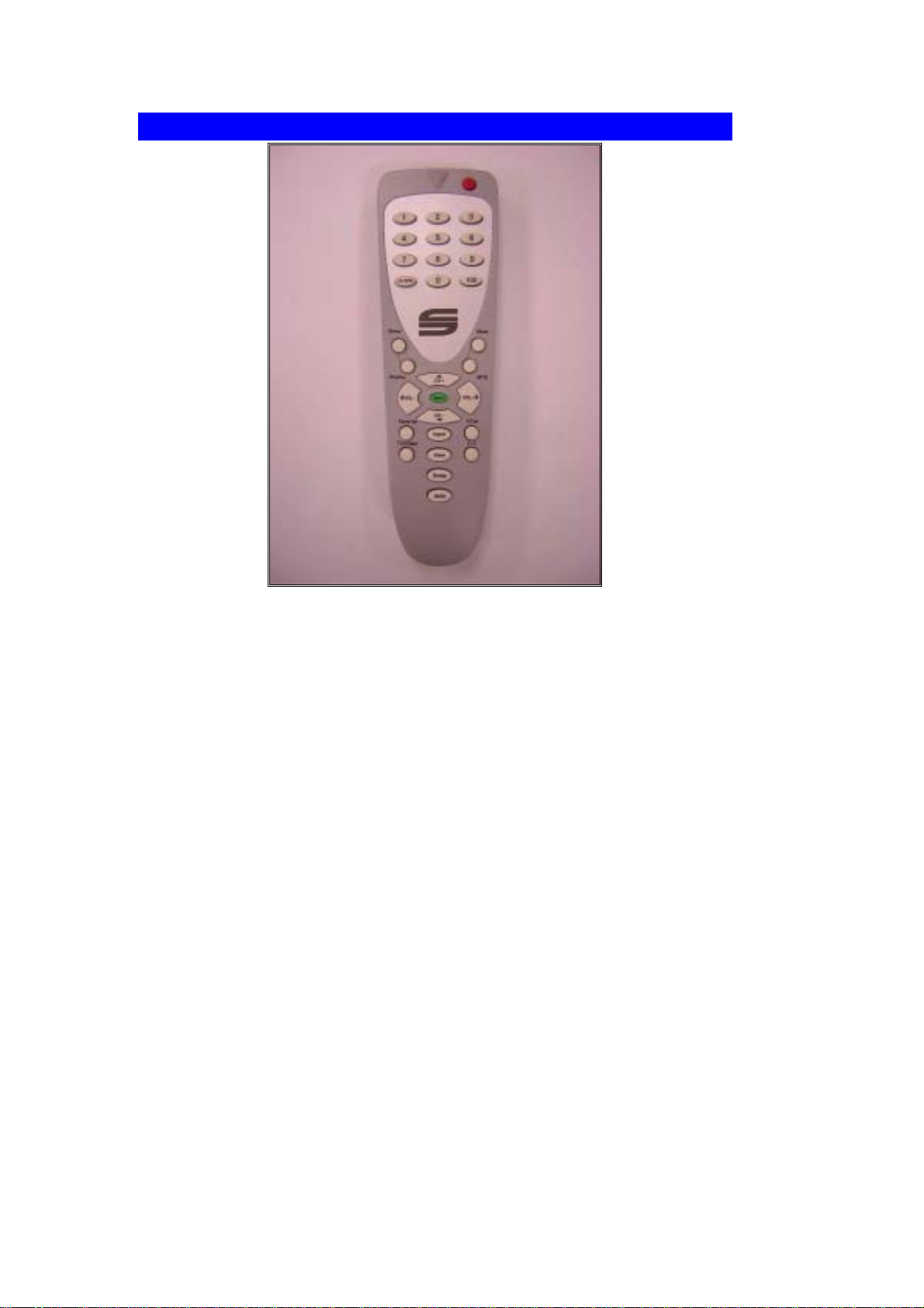
19. Remote Control
P/N: P16000410000
23
Page 25

2.4 Connector Pin Definition
SYSTEM BOARD
Function: VGA signal port
Connector type:
Specification: CNNT-HD D Sub-H-F-3Row-15pin-Dip-BLU
Pin Definition
Pin No. Pin Name I/O Description
1 VGAR I 75 ohm termination, 0.7Vp-p red signal
2 VGAG I 75 ohm termination, 0.7Vp-p green signal
3 VGAB I 75 ohm termination, 0.7Vp-p blue signal
4 GND - GND 5 NC - No connection
6 GND - GND
7 GND - GND
8 GND - GND
9 VGA5V I VCC 5V IN
10 GND - GND
11 GND - 12 VGASDA I/O I2C data bus for Reading DDC data
13 VGA_HS I Horizontal Frequency
14 VGA_VS I Vertical Frequency
15 VGASCL I I2C clock bus for Reading DDC data
Function: DVI signal port
Connector type:
Specification: CNNT-DVI-H-29PIN-1.9mm-1.5A-WHITE-dip
Pin Definition
Pin No. Pin Name I/O Description
1 RX2m I TMDS LVDS input signal
2 RX2p I TMDS LVDS input signal
3 GND - GND
4 NC - No connection
5 NC - No connection
6 DDC_CLK I I2C clock bus for Reading DDC data
7 DDC_DATA I/O I2C data bus for Reading DDC data
24
Page 26

8 NC - No connection
9 RX1m I TMDS LVDS input signal
10 RX1p I TMDS LVDS input signal
11 GND - GND
12 NC - No connection
13 NC - No connection
14 GDC5V VCC 5V
15 GND GND
16 HOTPLG VCC 5V
17 RX0m TMDS LVDS input signal
18 RX0p TMDS LVDS input signal
19 GND GND
20 NC - No connection
21 NC - No connection
22 GND GND
23 RXCp TMDS LVDS input clock
24 RXCm TMDS LVDS input clock
25 NC - No connection
26 NC - No connection
27 NC - No connection
28 NC - No connection
29 AGND - GND
30 AGND - GND
Function: PC Audio In
Connector type:
Specification: CNNT-EAR Phone Jack-H-F-5pin-3.6ψ-Dip
Pin Definition
Pin No. Pin Name I/O Description
1 AUD_R I Audio In_R
2 GND - GND
3 GND - GND
4 AUD_L I Audio In_L
5 GND - GND
Function: RS-232 port
25
Page 27

Connector type:
Specification: CNNT-Mini Din-H-F-8pin-12ψ-Dip
Pin Definition
Pin No. Pin Name I/O Description
1 NC - No connection
2 NC - No connection
3 GND - GND
4 NC - No connection
5 NC - No connection
6 NC - No connection
7 PC_TXD I/O RS-232 protocl
8 PC_RXD I/O RS-232 protocl
9 GND - GND
10 GND - GND
11 GND - GND
Function: Audio Out
Connector type: Push Terminal
Specification: CNNT-PUSH TERMINAL-F DIP RIGHT ANGLE-4 PIN-5mm
Pin Definition
Pin No. Pin Name I/O Description
1 Speaker/PR O Audio Out_R
2 Speaker/PL O Audio Out_L
3 GND - GND
4 GND - GND
Function: Interface In
Connector type:
Specification: CNNT-CENTRONIC DIP RIGHT ANGLE-M-50 pin-2.16 mm
Pin Definition
Pin No. Pin Name I/O Description
1 IF_EN I Connection test
2 AV9_MUX
26
Page 28

3 V5_IF VCC 5V
4 GND - GND
5 GND - GND
6 OCVBS_SC1 O AV Out1
7 RIN_SC1 I SCART RGB_R IN
8 GIN_SC1 I SCART RGB_G IN
9 BIN_SC1 I SCART RGB_B IN
10 GND - GND
11 HD_Y I HDTV_Y IN
12 HD_PB I HDTV_PB IN
13 HD_PR I HDTV_PR IN
14 GND - GND
15 GND - GND
16 ALO_SC2 O Audio Out_L SCART2
17 ARO_SC2 O Audio Out_R SCART2
18 ALO_SC1 O Audio Out_L SCART1
19 ARO_SC1 O Audio Out_R SCART1
20 GND - GND
21 YCBCR_L I Audio In_L YCBCR
22 YCBCR_R I Audio In_R YCBCR
23 HDTV_L I Audio In_L HDTV
24 HDTV_R I Audio In_R HDTV
25 GND GND
26 GND GND
27 CVBS_SC1 I AV IN
28 IF_YCVBS I S-VIDEO_Y IN
29 IF_C I S-VIDEO_C IN
30 GND - GND
31 OCVBS_SC2 O AV Out2
32 IF_VCR I YCBCR_CR IN
33 IF_VCB I YCBCR_CB IN
34 IF_VY I YCBCR_Y IN
35 GND - GND
36 SCL_5V I I2C clock bus for selecting scart connectors
37 SDA_5V I/O I2C data bus for selecting scart connectors
38 TPA_MODE O EARPHONE TEST
39 GND - GND
40 EPOUT_L O EARPHONE Out_L
27
Page 29

41 EPOUT_R O EARPHONE Out_R
42 AMP_WF O Sub_Woofer Out
43 LINE_L O LINE Out_L
44 LINE_R O LINE Out_R
45 GND - GND
46 SAL_SC2 I AUDIO IN_L (S-VIDEO)
47 SAR_SC2 I AUDIO IN_R (S-VIDEO)
48 CVBSAL_SC1 I AUDIO IN_L (AV)
49 CVBSAR_SC1 I AUDIO IN_L (AV)
50 GND - GND
Function: Tuner In
Connector type: FX2-40P-1.27DS
Specification: CNNT-Dip Right Angle-M-40PIN-1.27mm-0.5A
Pin Definition
Pin No. Pin Name I/O Description
1 GND - GND
2 T1_RED I CC ,V-Chip RED In
3 T1_GRE I CC ,V-Chip GREEN In
4 T1_BLU I CC ,V-Chip BLUE In
5 GND - GND
6 VPC1_T1HS O CC ,V-Chip H Sync Out
7 VPC1_T1VS O CC ,V-Chip V Sync Out
8 GND - GND
9 T1_SIF I Tuner1 Audio In
10 T2_SIF I Tuner2 Audio In
11 GND - GND
12 T2_RED I CC ,V-Chip RED In
13 T2_GRE I CC ,V-Chip GREEN In
14 T2_BLU I CC ,V-Chip BLUE In
15 GND - GND
16 VPC2_T2HS O CC ,V-Chip H Sync Out
17 VPC2_T2VS O CC ,V-Chip V Sync Out
18 VPC2_T2CV O AV2 Feedback signal
19 VCC O DC Power 5V
20 TUNER_EN I Tuner Test Signal
28
Page 30

21 GND - GND
22 T1_CVBS I AV1 In
23 T1_FB I CC,V-Chip OSD Timing Signal In
24 GND - GND
25 VPC1_T1CV O AV1 Feedback signal
26 GND - GND
27 VVINT I CC,V-Chip Interrupt In
28 RESETn O TT1 Reset Signal
29 GVINT I CC,V-Chip Interrupt In
30 GND - GND
31 VSCL O I2C Clock bus for V-Port
32 VSDA I/O I2C Data bus for V-Port
33 SCL O I2C Clock bus for G-Port
34 SDA I/O I2C Data bus for V-Port
35 GND - GND
36 T2_FB I CC,V-Chip OSD Timing Signal In
37 T2_CVBS I AV2 In
38 GND - GND
39 VCC O DC Power 5V
40 GND - GND
Function: LVDS output port
Connector type: LVDS-30pin
Specification: CNNT-LVDS-F SMD STRAIGHT-V-30 PIN-1.25mm
Pin Definition
Pin No. Pin Name I/O Description
1
2 NC - No connection
3 NC - No connection
4 NC - No connection
NC - No connection
5 NC - No connection
6 NC - No connection
7 NC - No connection
8 GND - GND
9 TXE3p O Positive LVDS differential data output. Ch 3
10 TXE3m O Negative LVDS differential data output. Ch 3
29
Page 31

11 TXECKp O Positive LVDS differential clock output.
12 TXECKm O Negative LVDS differential clock output
13 GND - GND
14 GND - GND
15 TXE2p O Positive LVDS differential data output. Ch 2
16 TXE2m O Negative LVDS differential data output. Ch 2
17 TXE1p O Positive LVDS differential data output. Ch 1
18 TXE1m O Negative LVDS differential data output. Ch 1
19 TXE0p O Positive LVDS differential data output. Ch 0
20 TXE0m O Negative LVDS differential data output. Ch 0
21 GND - GND
22 GND - GND
23 GND - GND
24 GND - GND
25 GND - GND
26 VCC - +5.0V power supply
27 VCC - +5.0V power supply
28 VCC - +5.0V power supply
29 VCC - +5.0V power supply
30 VCC - +5.0V power supply
Function: Power Input 1
Connector type:
Specification: M15-I25002CNNT M 15PIN pitch 2.5mm DIP straight
Pin Definition
Pin No. Pin Name I/O Description
1 V7_SYS I DC Power 7V IN
2 V5_SYS I DC Power 5V IN
3 V5_SYS I DC Power 5V IN
4 V5_SYS I DC Power 5V IN
5 V5_SYS I DC Power 5V IN
6 GND - GND
7 GND - GND
8 GND - GND
9 GND - GND
10 V7_SYS I DC Power 7V IN
30
Page 32

11 GND - GND
12 LCD_INVON O Inverter On/Off
13 GND - GND
14 BRI O Backlight Brightness Control
15 GND - GND
Function: Power Input 2
Connector type:
Specification: M11-I25002CNNT M 11PIN pitch 2.5mm DIP straight
Pin Definition
Pin No. Pin Name I/O Description
1 V14_SYS I DC Power 14V IN
2 V14_SYS I DC Power 14V IN
3 V14_SYS I DC Power 14V IN
4 GND - GND
5 GND - GND
6 GND - GND
7 V12_SYS I DC Power 12V IN
8 GND - GND
9 V12_SYS I DC Power 12V IN
10 GND - GND
11 GND - GND
Function: Keypad In
Connector type:
Specification: CNNT F 15PIN DN-V 1.25mm SIM15
Pin Definition
Pin No. Pin Name I/O Description
1 5V_KEY1 I- DC +5V power input
2 GND GND
3 KEY_X1 O Signal sent from System to Keypad 1
4 KEY_X2 O Signal sent from System to Keypad 2
5 KEY_X3 O Signal sent from System to Keypad 3
6 KEY_Y1 I Signal sent from Keypad to System 1
31
Page 33

7 KEY_Y2 I Signal sent from Keypad to System 2
8 KEY_Y3 I Signal sent from Keypad to System 3
9 GND - GND
10 IRDATA1 I Signal sent from IR to Keypad
11 GND - GND
12 LED11 O Signal for LED 1
13 LED22 O Signal for LED 2
14 LED33 O Signal for LED 3
15 LED44 O Signal for LED 4
INTERFACE BOARD
Function: Interface Out Port
Connector type:
Specification: NNT-CENTRONIC DIP RIGHT ANGLE-M-50 pin-2.16 mm
Pin Definition
Pin No. Pin Name I/O Description
1 GND GND
2 NC - No connection
3 NC - No connection
4 GND - GND
5 GND - GND
6 NC - No connection
7 NC - No connection
8 NC - No connection
9 NC - No connection
10 GND - GND
11 YPbPr_ Pr O YPbPr_ Pr out
12 YPbPr _Pb O YPbPr _Pb out
13 YPbPr _ Y O YPbPr _ Y out
14 GND - GND
15 GND - GND
16 NC - No connection
17 NC - No connection
18 NC - No connection
19 NC - No connection
20 GND - GND
32
Page 34

21 AL2_YCbCr O Audio out_L YCBCR
22 AR2_YCbCr O Audio out_R YCBCR
23 AL1_ YPbPr O Audio out _L YPbPr
24 AR1_ YPbPr O Audio out _R YPbPr
25 GND GND
26 GND GND
27 CVBS_SC1 O AV out
28 YCVBS_SC2 O S-VIDEO_Y out
29 CIN_SC2 O S-VIDEO_C out
30 GND - GND
31 NC - No connection
32 YCBCR_CR O YCBCR_CR out
33 YCBCR_CB O YCBCR_CB out
34 YCBCR_Y O YCBCR_Y out
35 GND - GND
36 NC - No connection
37 NC - No connection
38 TPA_MODE I EARPHONE TEST
39 GND - GND
40 EAR_LOUT I EARPHONE Out_L
41 EAR_ROUT I EARPHONE Out_R
42 AMP_WFOUT I Sub_Woofer Out
43 LINE_LOUT I LINE Out_L
44 LINE_ROUT I LINE Out_R
45 GND - GND
46 SL_SC2 O AUDIO out_L (S-VIDEO)
47 SR_SC2 O AUDIO out _R (S-VIDEO)
48 CVBSAL_SC1 O AUDIO out _L (AV)
49 CVBSAR_SC1 O AUDIO out _R (AV)
50 GND - GND
Function: YPbPr & YcbCr Input Port
Connector type: RCA
Specification: CNNT-RCA*6Green Blue Red /Green Blue Red-F DIP RIGHT ANGLE 8.3ψ-9PIN-
Pin Definition
33
Page 35

Pin No. Pin Name I/O Description
1 YPbPr_Y I YPbPr _ Y out
2 YPbPr _Pb I YPbPr_ Pb out
3 YPbPr _Pr I YPbPr _Pr out
4 YCBCR_ Y I YCBCR_Y out
5 YCBCR_CB I YCBCR_CB out
6 YCBCR_CR I YCBCR_CR out
7 GND - GND
8 GND - GND
9 GND - GND
Function: Audio Input Port 1(for YPbPr & YcbCr)
Connector type: RCA
Specification: CNNT-RCA*4 Red White/Red White-F DIP RIGHT ANGLE 8.3ψ-6PIN
Pin Definition
Pin No. Pin Name I/O Description
1 AR1_ YPbPr I Audio IN _R YPbPr
2 AL1_ YPbPr I Audio IN _L YPbPr
3 AR2_YCbCr I Audio IN _R YCBCR
4 AL2_YCbCr I Audio IN _L YCBCR
5 GND - GND
6 GND - GND
Function: CVBS & S-VIDEO Input Port
Connector type:
Specification: CNNT-RCA*1 Yellow+S-VIDEO*1 Black-F DIP RIGHT ANGLE 8.3ψ-9PIN
Pin Definition
Pin No. Pin Name I/O Description
1 CIN_SC2 I S-VIDEO_C IN
2 YCVBS_SC2 I S-VIDEO_Y IN
3 GND O GND
4 GND O GND
5 CVBS_SC1 I AV IN
6 GND - GND
34
Page 36

7 GND - GND
8 GND - GND
9 GND - GND
Function: Audio Input Port 2(for CVBS & S-VIDEO)
Connector type: RCA
Specification: CNNT-RCA*4 Red White/Red White-F DIP RIGHT ANGLE 8.3ψ-6PIN
Pin Definition
Pin No. Pin Name I/O Description
1 CVBSAR_SC1 I AUDIO IN _R (AV)
2 CVBSAL_SC1 I AUDIO IN _L (AV)
3 SR_SC2 I AUDIO IN_R (S-VIDEO)
4 SL_SC2 I AUDIO IN_L (S-VIDEO)
5 GND - GND
6 GND - GND
Function: Audio Output Port (Sub-Woofer & Line Out_R)
Connector type: RCA
Specification: CNNT-RCA*2 Up-Black Down-Red-F DIP RIGHT ANGLE 8.3ψ-3PIN
Pin Definition
Pin No. Pin Name I/O Description
1 AMP_WFOUT O Sub_Woofer Out
2 LINE_ROUT O LINE Out_R
3 GND - GND
Function: EARPHONE Output
Connector type:
Specification: CNNT-EAR Phone Jack-H-F-5pin-3.6ψ-Dip
Pin Definition
Pin No. Pin Name I/O Description
1 EAR_ROUT O EARPHONE Output_R
2 GND - GND
35
Page 37

3 TPA_MODE - EARPHONE TEST
4 EAR_LOUT O EARPHONE Output_L
5 GND - GND
Function: Audio Output Port (Line Out_L)
Connector type: RCA
Specification: CNNT-RCA*1 F DIP RIGHT ANGLE WHITE-3 PIN -8.3ψ
Pin Definition
Pin No. Pin Name I/O Description
1 LINE_LOUT O LINE Out_L
TUNER BOARD
Function: Tuner Out
Connector type: FX2-40S-1.27DS
Specification: CNNT-Dip Right Angle-F -40PIN-1.27mm-0.5A
Pin Definition
Pin No. Pin Name I/O Description
1 GND - GND
2 T1_RED O CC ,V-Chip RED Out
3 T1_GRE O CC ,V-Chip GREEN Out
4 T1_BLU O CC ,V-Chip BLUE Out
5 GND - GND
6 VPC1_T1HS I CC ,V-Chip H Sync In
7 VPC1_T1VS I CC ,V-Chip V Sync In
8 GND - GND
9 T1_SIF O Tuner1 Audio Out
10 T2_SIF O Tuner2 Audio Out
11 GND - GND
12 T2_RED O CC ,V-Chip RED Out
13 T2_GRE O CC ,V-Chip GREEN Out
14 T2_BLU O CC ,V-Chip BLUE Out
15 GND - GND
16 VPC2_T2HS I CC ,V-Chip H Sync In
17 VPC2_T2VS I CC ,V-Chip V Sync In
36
Page 38

18 VPC2_T2CV I AV2 Feedback signal
19 VCC I DC Power 5V
20 GND - GND
21 GND - GND
22 T1_CVBS O AV1 Out
23 T1_FB O CC,V-Chip OSD Timing Signal Out
24 GND - GND
25 VPC1_T1CV I AV1 Feedback signal
26 GND - GND
27 VVINT O CC,V-Chip Interrupt Out
28 RESETn I TT1 Reset Signal
29 GVINT O CC,V-Chip Interrupt Out
30 GND - GND
31 VSCL I I2C Clock bus for V-Port
32 VSDA I/O I2C Data bus for V-Port
33 SCL I I2C Clock bus for G-Port
34 SDA I/O I2C Data bus for G-Port
35 GND - GND
36 T2_FB O CC,V-Chip OSD Timing Signal Out
37 T2_CVBS O AV2 Out
38 GND - GND
39 VCC I DC Power 5V
40 GND - GND
KEYPAD BOARD
Function: Keypad Out
Connector type:
Specification: CNNT F 15PIN DN-V 1.25mm SIM15
Pin Definition
Pin No. Pin Name I/O Description
1 5V_KEY1 I- DC +5V power input
2 GND GND
3 KEY_X1 I Signal sent from System to Keypad 1
4 KEY_X2 I Signal sent from System to Keypad 2
5 KEY_X3 I Signal sent from System to Keypad 3
6 KEY_Y1 O Signal sent from Keypad to System 1
37
Page 39

7 KEY_Y2 O Signal sent from Keypad to System 2
8 KEY_Y3 O Signal sent from Keypad to System 3
9 GND - GND
10 IRDATA1 I Signal sent from IR to Keypad
11 GND - GND
12 LED11 O Signal for LED 1
13 LED22 O Signal for LED 2
14 LED33 I Signal for LED 3
15 LED44 I Signal for LED 4
Function: IR IN
Connector type: Pin Header
Specification: CNNT-PIN HEADER-M DIP STRAIGHT-7pin-2.54mm
Pin No. Pin Name I/O
1 V5_KEY1 I- DC +5V power input
2 GND - GND
3 IRDAT I Signal sent from IR to Keypad
4 LED1 O Signal for LED 1
5 LED2 O Signal for LED 2
6 GND GND
7 GND GND
Pin Definition
Description
IR BOARD
Function: IR OUT
Connector type: Female Header
Specification: CNNT-PIN HEADER-M DIP STRAIGHT-7pin-2.54mm
Pin Definition
Pin No. Pin Name I/O Description
1 V5_KEY1 I- DC +5V power input
2 GND - GND
3 IRDAT O Signal sent from IR to Keypad
4 LED1 O Signal for LED 1
5 LED2 O Signal for LED 2
38
Page 40

6 GND GND
7 GND GND
39
Page 41

3. Schematic
3.0 Tuner Board
40
Page 42

3.1 Graph Port Tuner
41
Page 43

3.2 Interface Board
42
Page 44

3.3 IR Board
43
Page 45

3.4 Keypad Board
44
Page 46

3.5 System Board-1 Graph Interface
45
Page 47

3.6 System Board-2 Power Management
46
Page 48

3.7 System Board-3 PW181 Power Management
47
Page 49

3.8 System Board-4 DVI Receiver
48
Page 50

3.9 System Board-5 ADC
49
Page 51

3.10 System Board-6 A/V Switch
50
Page 52

3.11 System Board-7 3D Comb Filter
51
Page 53

3.12 System Board-8 Video Decoder (V Port)
52
Page 54

3.13 System Board-9 Video Decoder (G Port)
53
Page 55

3.14 System Board-10 Deinterlace
54
Page 56

3.15 System Board-11 SDRAM
55
Page 57

3.16 System Board-12 Image Processor
56
Page 58

3.17 System Board-13 Flash Memory
57
Page 59

3.18 System Board-14 Miscellaneous
58
Page 60

3.19 System Board-15 LVDS
59
Page 61

3.20 System Board-16 Audio DSP
60
Page 62

3.21 System Board-17 Class D Audio PA
61
Page 63

4. Troubleshooting
No Power
No Power
Check power plug is securely inserted into the power socket?
No
Power plug is securely
inserted into the power
socket.
Yes
1.Check Power to system Cable
2.Check System to Keypad Cable
3.Check Keypad and IR Board
confix?
Yes
If power on still failed, please
replace power module.
Please replace the cable
No
what cause the power on
failed.
62
Page 64

No Sound
No Sound
Check the speaker wire connector to system board?
Yes
Check the input source and audio
cable into the correct connector?
Yes
1.Keep OSD is not in mute mode.
2.Confirm the volume value is not 0.
3.Power off, and re-plug power socket again.
4.If items 1,2,3 have no problem, replace interface board or
system board.
No
No
Please connection the
speaker wire to system
board.
Confirm input source and
audio cable select to the
correct channel.
63
Page 65

No Source Input
RGB or video source can’t be found
Check OSD select correct?
Yes
Confirm input source and the
No
output of OSD select is
correct.
Check image signal input at system board or interface board.
Yes
Replace system board or interface board.
No
Check input source cable
connection into the
connector.
64
Page 66

Keypad Failed
Keypad no response
Yes
1.Check the cable of keypad to system board.
2.Check keypad founction.
3..If item 1,2 have no problem, please replace keypad board or
system board.
65
Page 67

IR Failed
IR no response
Check IR board connection in to keypad board?
Yes
Check remote control have energy?
Yes
No
No
Please connection the IR
board into keypad board.
Change remote
control battery.
Replace IR board
66
Page 68

LED Failed
LED are not bright
Check the cable of system board to keypad?
Yes
Check keypad and IR board confix?
Yes
No
No
Please connection the cable
of system board to keypad.
Please connection the IR
board into keypad board.
Replace IR board.
67
Page 69

5. Firmware upgrade applications
Installation file: Flashupgrader.exe
COM port setting: COM1 as default
A specific directory for update:
There are some files should be in this directory. (bootcode.hex, configdata.hex, flasher.hex, gui.hex,
romcode.hex, and FlashAll.inf)
In a new version firmware, FlashAll.inf is the same. The files of Hex depend on the different firmware
version.
Cable switch: on System(S)side
Power cord: Plug out before update
a. Insert RS232 cable in Mouse socket or RS232 socket and make sure the power cord is out of AC
inlet.
b. Execute Flashupgrader.exe then click the button of Choose on the top of display.
c. Open FlashAll.inf in the specific directory and then click the button of Flash. This indicator of this
button will swap to Cancel instead of Flash. A message of Waiting for target reset is also showed.
d. Insert the power cord, and the update will be executed automatically.
e. After the whole process of update, the indicator of Close will appear again. Plug out the power cord
as a reset to the TV, and the new firmware is ready.
Remark: Serial
connection, 115200 Baud Rate, COM1, and Flash mode are the default in this execution.
68
Page 70

6. Standard Operation Procedure
6.0 Module assembly process
Step 1. Stand module loose
69
Page 71

Step 2. Tuner module and Interface module assembly
70
Page 72

Step3. Label stick
71
Page 73

6.1 Module repair process
6.1.1 Tuner & Interface module
72
Page 74

6.1.2 Stand module
73
Page 75

6.1.3 Back Cover & Speaker module
74
Page 76

6.1.4 PCBA module
75
Page 77

6.1.5 Power module
76
Page 78

6.1.6 LCD module
77
 Loading...