

Page 1

EGOFOOLLER
MT1389EE-L1 (DVDM ASSY : IC201)
For Education by EgoFooller
• DVD IC
Pin Arrangement
IREF
AVDD3
RFGC
OSP
OSN
CRTPLP31RFRPDC32RFRPAC
CEQN
CEQP
RFGN D
HRFZC
ADCVSS
ADCVDD3
RFVDD3
S_VREFN
LPFIN
LPFOP
LPFIP
LPFON
S_VCM
S_VREFP
XTALI
XTALO
JITFN
JITFO
PLLVSS
IDACEXLP
PLLVDD3
ASDATA4
RFVDD18
RFGND18
DVSS
SPDIF
MC_DATA
DVSS
ABCK
ASDATA2
ASDATA1
ALRCK
ASDATA0
ACLK
ASDATA3
DVDD18
SPLRCK
SPDATA
SPBCK
DVDD3
YUV6/ R
HSYN / V_ADIN2
VSYN / V_ADIN1
SPMCLK
YUV5/B
YUV7
DVDD3
YUV2 /C
DACVDDA
YUV3/CVBS
YUV1 /Y
DACVSSB
DACVDDB
DACVSSC
DACVSSA
YUV4 /G
AGND
DVDA
DVDB
DVDC
DVDD
DVDRFIP
DVDRFIN
CDFON
CDFOP
MDI1
MDI2
LDO2
LDO1
SVDD3
CSO / RFOP
RFLVL / RFON
SGND
V2REFO
V20
VREFO
FEO
TEO
TEZISLV
OP_OUT
OP_INN
OP_INP
DMO
FMO
TROPENPWM
PWMOUT1 / V_ADIN9
TRO
FOO
USB_VSS
USBP
USBM
USB_VDD3
FG / V_ADIN8
TDI / V_ADIN4
TMS / V_ADIN5
TCK / V_ADIN6
TDO / V_ADIN7
DVDD18
IOA2
IOA3
IOA4
IOA5
IOA6
IOA7
HIGHA0
IOA18
IOA19
DVSS
APLLCAP
APLLVSS
251
256
255
254
253
252
1
2
3
4
5
6
7
MA
8
MB
9
MC
10
MD
11
SA
12
SB
13
SC
14
SD
15
16
17
TNI
18
TPI
19
20
21
22
23
24
25
26
27
28
29
30
33
34
35
36
37
38
39
40
41
42
43
44
45
46
47
48
49
50
51
52
53
54
55
56
57
58
59
60
61
62
63
64
6566676869
250
70
71
244
243
241
236
235
233
249
248
247
246
245
242
240
239
238
237
73
74
72
75767778798081828384858687888990919293949596979899
231
234
232
230
229
228
227
226
225
219
224
223
222
221
220
218
100
101
102
103
212
211
209
204
203
201
199
196
195
194
217
216
215
214
213
210
208
207
206
205
202
200
104
105
106
107
108
109
110
111
112
113
114
115
116
117
118
121
122
119
120
193
198
197
192
YUV0/CIN
191
FS
VREF
190
189
DACVDDC
188
RD16
187
RD17
186
RD18
185
RD19
184
RD20
183
RD21
182
DVDD3
181
RD22
180
RD23
179
DQM2
178
DQM3
177
RD24
176
RD25
175
DVSS
174
RD26
173
DVDD18
172
RD27
171
RD28
170
RD29
169
RD30
168
RD31
167
DVDD3
166
RA4
165
RA5
164
RA6
163
DVSS
162
RA7
161
DVSS
160
RA8
159
RA9
158
RA11
157
CKE
156
RCLK
155
DVDD3
154
RCLKB
153
RVREF / V_ADIN 3
152
DVDD18
151
RA3
150
RA2
149
RA1
148
DVSS
147
RA0
146
RA10
145
BA1
144
DVSS
143
BA0
142
RCS#
141
DVDD3
140
RAS#
139
CAS#
138
RWE#
137
DQM1
136
DQS1
135
RD8
134
DVSS
133
RD9
132
RD10
131
RD11
130
RD12
129
RD13
123
124
125
126
127
128
A16
IOWR#
APLLVD D3
HIGHA3
HIGHA5
HIGHA4
HIGHA6
HIGHA7
DVDD3
IOA1
IOA20
IOCS#
IOO E#
DVDD3
HIGHA1
HIGHA2
AD4
AD1
AD0
AD3
AD2
DVSS
AD5
AD6
A17
ALE
AD7
IOA0
URD#
DVSS
UWR#
UP1_2
UP1_3
DVDD18
IOA21 / V_ADIN0
UP3_ 1
UP1_7
UP3_0
UP1_4
UP1_5
UP1_6
IR
ICE
INT0 #
DVDD3
DQM0
PRST#
UP3_ 5
UP3_ 4
RD4
RD6
RD3
RD1
RD7
RD5
DVSS
DQS0
DVSS
RD0
RD2
RD14
RD15
DVDD3
DVDD18
Page 2
EGOFOOLLER
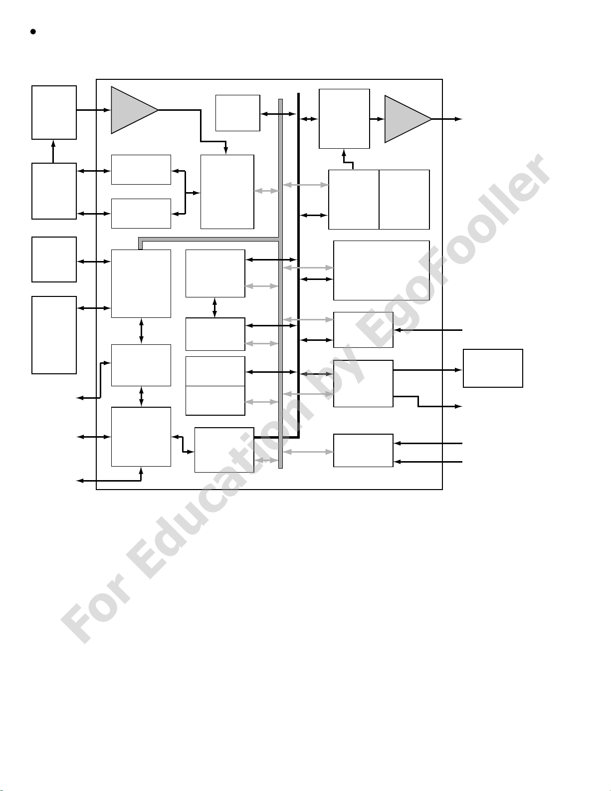
Block Diagram
For Education by EgoFooller
DVD
PUH
Module
Motor
Drive
Flash ROM
DRAM
USB
RF
Amplifier
Servo I/O
Spindle
Control
Memory
Controller
USB
Controller
Debug
Por t
Servo
Processor
Audio
DSP
SACD
Processor
System
Parser
CPPM/CPRM
DRM
108 MHz
TV Encoder
Video
Processor
Video Decoder
Video
Input
Audio
Output
Video
Deinterlacer
MPEG-1/2
MPEG-4
JPEG
DAC
PCM / DSD
CVBS, Y/C
Component Video
CCIR601/65
Audio
DAC
SPDIF
GPIO
IR/VFD
System
CPU
30-bit
RISC
Audio
Input
I2S
MIC
Page 3
EGOFOOLLER
Pin Function
For Education by EgoFooller
RF Interface (28)
No. Name Alt. I/O Function
226 RFGND18 Ground Analog ground
227 RFVDD18 Power Analog power 1.8V
250 CEQP Analog output EQ offset loop capacitance
251 CEQN Analog output EQ offset loop capacitance
252 OSP Analog output RF Offset cancellation capacitor connecting
253 OSN Analog output RF Offset cancellation capacitor connecting
254 RFGC Analog output RF AGC loop capacitor connecting for DVD-ROM
255 IREF Analog Input
256 AVDD3 Power Analog power 3.3V
1 AGND Ground Analog ground
2 DVDA Analog Input AC coupled input path A
3 DVDB Analog Input AC coupled input path B
4 DVDC Analog Input AC coupled input path C
5 DVDD Analog Input AC coupled input path D
6 DVDRFIP Analog Input AC coupled DVD RF signal input RFIP
7 DVDRFIN Analog Input AC coupled DVD RF signal input RFIN
8MA Analog Input DC coupled main-beam RF signal input A
9MB Analog Input DC coupled main-beam RF signal input B
10 MC Analog Input DC coupled main-beam RF signal input C
11 MD Analog Input DC coupled main-beam RF signal input D
12 SA Analog Input DC coupled sub-beam RF signal input A
13 SB Analog Input DC coupled sub-beam RF signal input B
14 SC Analog Input DC coupled sub-beam RF signal input C
15 SD Analog Input DC coupled sub-beam RF signal input D
16 CDFON Analog Input CD focusing error negative input
17 CDFOP Analog Input CD focusing error positive input
18 TNI Analog Input 3 beam satellite PD signal negative input
19 TPI Analog Input 3 beam satellite PD signal positive input
Current reference input. It generates reference current for RF path.
Connect an external 15K resistor to this pin and AVSS.
ALPC (4)
No. Name Alt. I/O Function
20 MDI1 Analog Input Laser power monitor input
21 MDI2 Analog Input Laser power monitor input
22 LDO2 Analog Output Laser driver output
23 LDO1 Analog Output Laser driver output
ADC for SACD (5)
No. Name Alt. I/O Function
239 ADCVDD3 Power Analog 3.3V Power for ADC
240 S_VCM Analog Inout SACD- Common mode reference
241 ADCVSS Ground Analog ground for ADC
242 S_VREFP Analog Inout SACD- TOP Reference
243 S_VREFN Analog Inout SACD- Bottom Reference
Reference Voltage (3)
No. Name Alt. I/O Function
28 V2REFO Analog output Reference voltage 2.8V
29 V20 Analog output Reference voltage 2.0V
30 VREFO Analog output Reference voltage 1.4V
Page 4
EGOFOOLLER
Analog Monitor Output (7)
For Education by EgoFooller
No. Name Alt. I/O Function
24 SVDD3 Power Analog power 3.3V
25 CSO RFOP Analog output Central servo Positive main beam summing output
26 RFLVL RFON Analog output RFRP low pass, or Negative main beam summing output
27 SGND Ground Analog ground
31 FEO Analog output Focus error monitor output
32 TEO Analog output Tracking error monitor output
33 TEZISLV Analog output TE Slicing Level
Analog Servo Interface (6)
No. Name Alt. I/O Function
244 RFVDD3 Power Analog Power
245 RFRPDC Analog output RF ripple detect output
246 RFRPAC Analog Input RF ripple detect input(through AC-coupling)
247 HRFZC Analog Input High frequency RF ripple zero crossing
248 CRTPLP Analog output Defect level filter capacitor connecting
249 RFGND Ground Analog Ground
RF Data PLL Interface (9)
No. Name Alt. I/O Function
230 JITFO Analog output The output terminal of RF jitter meter.
231 JITFN Analog Input The input terminal of RF jitter meter.
232 PLLVSS Ground Ground pin for data PLL and related analog circuitry.
233 IDACEXLP Analog output Data PLL DAC Low-pass filter
234 PLLVDD3 Power Power pin for data PLL and related analog circuitry.
235 LPFON Analog Output The negative output of loop filter amplifier
236 LPFIP Analog Input The positive input terminal of loop filter amplifier.
237 LPFIN Analog Input The negative input terminal of loop filter amplifier.
238 LPFOP Analog Output The positive output of loop filter amplifier
Motor and Actuator Driver Interface (10)
No. Name Alt. I/O Function
34 OP_OUT Analog output Op amp output.
35 OP_INN Analog input Op amp negative input
36 OP_INP Analog input Op amp positive input
37 DMO Analog Output Disk motor control output. PWM output.
38 FMO Analog Output Feed motor control. PWM output.
39 TROPENPWM Analog Output Tray PWM output / Tray open output.
40 PWMOUT1 V_ADIN9 Analog Output 1st General PWM output, or Version AD input 9
41 TRO Analog Output Tracking servo output. PDM output of tracking servo compensator.
42 FOO Analog Output Focus servo output. PDM output of focus servo compensator
LVTTL 3.3V Input,
47 FG (Digital pin) V_ADIN8
Schmitt Input,
pull-up , with
analog input path
for V_ADIN8
Motor Hall sensor input, or Version AD input 8
Page 5
EGOFOOLLER
General Power / Ground (32)
For Education by EgoFooller
No. Name Alt. I/O Function
52, 97, 122,
152, 173, 221
85, 116, 144,
163, 216
73, 80, 108,
127, 141, 155,
167, 182, 212
62, 94, 119,
134, 148, 161,
175, 223
204 DVDD3 Power 3.3V power pin Video DAC digital circuitry only
63 APLLCAP Analog Inout APLL External Capacitance connection
64 APLLVSS Ground Ground pin for audio clock circuitry
65 APLLVDD3 Power 3.3V Power pin for audio clock circuitry
Micro Controller and Flash Interface (48)
No. Name Alt. I/O Function
59 HIGHA0 Inout, 2-16MA, SR, PU Microcontroller address 8
75 HIGHA1 Inout, 2-16MA, SR, PU Microcontroller address 9
74 HIGHA2 Inout, 2-16MA, SR, PU Microcontroller address 10
72 HIGHA3 Inout, 2-16MA, SR, PU Microcontroller address 11
71 HIGHA4 Inout, 2-16MA, SR, PU Microcontroller address 12
70 HIGHA5 Inout, 2-16MA, SR, PU Microcontroller address 13
69 HIGHA6 Inout, 2-16MA, SR, PU Microcontroller address 14
68 HIGHA7 Inout, 2-16MA, SR, PU Microcontroller address 15
91 AD7 Inout, 2-16MA, SR Microcontroller address/data 7
88 AD6 Inout, 2-16MA, SR Microcontroller address/data 6
87 AD5 Inout, 2-16MA, SR Microcontroller address/data 5
86 AD4 Inout, 2-16MA, SR Microcontroller address/data 4
84 AD3 Inout, 2-16MA, SR Microcontroller address/data 3
83 AD2 Inout, 2-16MA, SR Microcontroller address/data 2
82 AD1 Inout, 2-16MA, SR Microcontroller address/data 1
81 AD0 Inout, 2-16MA, SR Microcontroller address/data 0
93 IOA0 Inout, 2-16MA, SR, PU Microcontroller address 0 / IO
78 IOA1 Inout, 2-16MA, SR, PU Microcontroller address 1 / IO
53 IOA2 Inout, 2-16MA, SR, PU Microcontroller address 2 / IO
54 IOA3 Inout, 2-16MA, SR, PU Microcontroller address 3 / IO
55 IOA4 Inout, 2-16MA, SR, PU Microcontroller address 4 / IO
56 IOA5 Inout, 2-16MA, SR, PU Microcontroller address 5 / IO
57 IOA6 Inout, 2-16MA, SR, PU Microcontroller address 6 / IO
58 IOA7 Inout, 2-16MA, SR, PU Microcontroller address 7 / IO
67 A16 Output, 2-16MA, SR Flash address 16
92 A17 Output, 2-16MA, SR Flash address 17
60 IOA18 Inout, 2-16MA, SR, SMT Flash address 18 / IO
61 IOA19 Inout, 2-16MA, SR, SMT Flash address 19 / IO
76 IOA20 Inout, 2-16MA, SR, SMT Flash address 20 / IO
89 IOA21 V_ADIN0
DVDD18 Power 1.8V power pin for internal digital circuitry
DVSS Ground 1.8V Ground pin for internal digital circuitry
DVDD3 Power 3.3V power pin for internal digital circuitry
DVSS Ground 3.3V Ground pin for internal digital circuitry
Flash address 21 / IO
Inout, 2-16MA,
SR, SMT
While External FLASH size <= 2MB:
Version AD input port 0, or
GPIO
Page 6

EGOFOOLLER
No. Name Alt. I/O Function
For Education by EgoFooller
90 ALE
79 IOOE# Inout, 2-16MA, SR, SMT Flash output enable, active low / IO
66 IOWR# Inout, 2-16MA, SR, SMT Flash write enable, active low / IO
77 IOCS#
95 UWR#
96 URD#
98 UP1_2 Inout, 4MA, SR, PU, SMT Microcontroller port 1-2
99 UP1_3 Inout, 4MA, SR, PU, SMT Microcontroller port 1-3
100 UP1_4 Inout, 4MA, SR, PU, SMT Microcontroller port 1-4
101 UP1_5 Inout, 4MA, SR, PU, SMT Microcontroller port 1-5
102 UP1_6 SCL Inout, 4MA, SR, PU, SMT
103 UP1_7 SDA Inout, 4MA, SR, PU, SMT
104 UP3_0 RXD Inout, 4MA, SR, PU, SMT
105 UP3_1 TXD Inout, 4MA, SR, PU, SMT
Inout, 2-16MA,
SR, PU, SMT
Inout, 2-16MA,
SR, PU, SMT
Inout, 2-16MA,
SR, PU, SMT
Inout, 2-16MA,
SR, PU, SMT
Microcontroller address latch enable
Flash chip select, active low / IO
Microcontroller write strobe, active low
Microcontroller read strobe, active low
Microcontroller port 1-6
2
I
C clock pin
Microcontroller port 1-7
2
I
C data pin
Microcontroller port 3-0
8032 RS232 RXD
Microcontroller port 3-1
8032 RS232 TXD
106 UP3_4 RXD SCL Inout, 4MA, SR, PU, SMT
107 UP3_5 TXD SDA Inout, 4MA, SR, PU, SMT
111 IR Input, SMT IR control signal input
112 INT0#
Inout, 2-16MA,
SR, PU, SMT
Microcontroller port 3-4
Hardwired RD232 RXD
2
I
C clock pin
Microcontroller port 3-5
Hardwired RD232 TXD
2
I
C data pin
Microcontroller external interrupt 0, active low
Page 7

EGOFOOLLER
Audio Interface (14)
For Education by EgoFooller
No. Name Alt. I/O Function
Audio DAC master clock of SPDIF input
208 SPMCLK SCLK0 Inout
209 SPDATA SDIN0 Inout
210 SPLRCK SDO0 Inout
211 SPBCK
213 ALRCK
214 ABCK Fs64
215 ACLK Inout, 4MA Audio DAC master clock
217 ASDATA0
218 ASDATA1
219 ASDATA2
220 ASDATA3
222 ASDATA4 INT1#
224 MC_DATA INT2# Inout
225 SPDIF
SDCS0
ASDATA5
Inout
Inout
4MA, PD, SMT
Output
4MA
Inout, 4MA,
PD SMT
Inout, 4MA,
PD SMT
Inout, 4MA,
PD SMT
Inout, 4MA,
PD SMT
Inout, 4MA,
PD SMT
Output, 2-16MA,
SR : ON/OFF
While SPDIF input is not used:
Serial interface port 0 clock pin
GPIO
Audio data of SPDIF input
While SPDIF input is not used:
Serial interface port 0 data-in
GPIO
Audio left/right channel clock of SPDIF input
While SPDIF input is not used:
Serial interface port 0 data-out
GPIO
Audio bit clock of SPDIF input
While SPDIF input is not used:
Serial interface port 0 chip select
Audio serial data 5 part I : DSD data sub-woofer
channel or Microphone output
GPIO
Audio left/right channel clock
Trap value in power-on reset:
1 : use external 373
0: use internal 373
Audio bit clock
Phase de-modulation
Audio serial data 0 (Front-Left/Front-Right)
DSD data left channel
Trap value in power-on reset :
1 : manufactory test mode
0 : normal operation
Audio serial data 1 (Left-Surround/Right-Surround)
DSD data right channel
Trap value in power-on reset :
1 : manufactory test mode
0 : normal operation
While only 2 channels output:
GPIO
Audio serial data 2 (Center/LFE)
DSD data left surround channel
Trap value in power-on reset :
1 : manufactory test mode
0 : normal operation
While only 2 channels output:
GPIO
Audio serial data 3 (Center-back/ Center-left-back/Center-right-back, in 6.1 or
7.1 mode)
DSD data right surround channel
Trap value in power-on reset :
1 : manufactory test mode
0 : normal operation
While only 2 channels output:
GPIO
Audio serial data 4 (Down-mixed Left/Right)
DSD data center channel
Trap value in power-on reset :
1 : manufactory test mode
0 : normal operation
While only 2 channels output:
Microcontroller external interrupt 1
GPIO
Microphone serial input
While not support Microphone:
Microcontroller external interrupt 2
GPIO
SPDIF output
Page 8

EGOFOOLLER
Video Interface (18)
For Education by EgoFooller
No. Name Alt. I/O Function
189 DACVDDC Power 3.3V power pin for VIDEO DAC circuitry
190 VREF Analog Bandgap reference voltage
191 FS Analog Full scale adjustment
192 YUV0 CIN
193 DACVSSC Ground Ground pin for VIDEO DAC circuitry
194 YUV1 Y
195 DACVDDB Power 3.3V power pin for VIDEO DAC circuitry
196 YUV2 C
197 DACVSSB Ground Ground pin for VIDEO DAC circuitry
198 YUV3 CVBS
199 DACVDDA Power 3.3V power pin for VIDEO DAC circuitry
200 YUV4 Y/G
201 DACVSSA Ground Ground pin for VIDEO DAC circuitry
202 YUV5 B/Cb/Pb
203 YUV6 R/Cr/Pr
205 VSYN V_ADIN1
206 YUV7
207 HSYN
INT3#
ASDATA5
INT4#
V_ADIN2
Output
4MA, SR
Output
4MA, SR
Output
4MA, SR
Output
4MA, SR
Output
4MA, SR
Output
4MA, SR
Output
4MA, SR
Inout
4MA, SR
SMT
Inout
4MA, SR
SMT
Inout
4MA, SR
SMT
Video data output bit 0
Compensation capacitor
Video data output bit 1
Analog Y output
Video data output bit 2
Analog chroma output
Video data output bit 3
Analog composite output
Video data output bit 4
Green or Y
Video data output bit 5
Blue or CB
Video data output bit 6
Red or CR
Vertical sync input/output
While no External TV-encoder:
Vertical sync for video-input
Version AD input port 1
GPIO
Video data output bit 7
While no External TV-encoder:
Microcontroller external interrupt 3
Audio serial data 5 part II : DSD data sub-woofer channel or Microphone
output
GPIO
Horizontal sync input/output
While no External TV-encoder:
Horizontal sync for video-input
Microcontroller external interrupt 4
Version AD input port 2
GPIO
MISC (8)
No. Name Alt. I/O Function
43 USB_VSS USB Ground USB ground pin
44 USBP Analog Inout USB port DPLUS analog pin
45 USBM Analog Inout USB port DMINUS analog pin
46 USB_VDD3 USB Power USB Power pin 3.3V
110 PRST# Input PU, SMT Power on reset input, active low
109 ICE Input PD, SMT Microcontroller ICE mode enable
228 XTALO Output 27M crystal out
229 XTALI Input 27M crystal in
Page 9

EGOFOOLLER
DRAM Interface (63)(sorted by position)
For Education by EgoFooller
No. Name Alt. I/O Function
DRAM data 16
188 RD16
187 RD17
186 RD18
185 RD19
184 RD20
183 RD21
181 RD22
180 RD23
179 DQM2 YUVIN7
178 DQM3
177 RD24
176 RD25
LLC_CLK
SMPTE_C[0]
YUVIN0
SMPTE_C[1]
YUVIN1
SMPTE_C[2]
YUVIN2
SMPTE_C[3]
YUVIN3
SMPTE_C[4]
YUVIN4
SMPTE_C[5]
YUVIN5
SMPTE_C[6]
YUVIN6
SMPTE_C[7]
INT6#
SMPTE_CLK
USB_CLK
SDIN1
MS_BS
SMPTE_Y[0]
SDO1
MS_SDIO
SMPTE_Y[1]
Inout
Pull-Down
Inout
Pull-Down
Inout
Pull-Down
Inout
Pull-Down
Inout
Pull-Down
Inout
Pull-Down
Inout
Pull-Down
Inout
Pull-Down
Inout
Pull-Up
Inout
Pull-Up
Inout
Non-pull
Inout
Non-pull
While using 16-bits wide DRAM:
Line Locked Clock input/output
Digital Video output C bit 0
GPIO
DRAM data 17
While using 16-bits wide DRAM:
Video input data 0
Digital Video output C bit 1
GPIO
DRAM data 18
While using 16-bits wide DRAM:
Video input data 1
Digital Video output C bit 2
GPIO
DRAM data 19
While using 16-bits wide DRAM:
Video input data 2
Digital Video output C bit 3
GPIO
DRAM data 20
While using 16-bits wide DRAM:
Video input data 3
Digital Video output C bit 4
GPIO
DRAM data 21
While using 16-bits wide DRAM:
Video input data 4
Digital Video output C bit 5
GPIO
DRAM data 22
While using 16-bits wide DRAM:
Video input data 5
Digital Video output C bit 6
GPIO
DRAM data 23
While using 16-bits wide DRAM:
Video input data 6
Digital Video output C bit 7
GPIO
Data Mask 2
While using 16-bits wide DRAM:
Video input data 7
GPIO
Data Mask 3
While using 16-bits wide DRAM:
Microcontroller external interrupt 6
Digital Video output Clock
USB port CLK input (48MHz) part II
GPIO
DRAM data 24
While using 16-bits wide DRAM:
Serial interface port 1 data-in
MS Card BS pin part II
Digital Video output Y bit 0
GPIO
DRAM data 25
While using 16-bits wide DRAM:
Serial interface port 1 data-out
MS Card SDIO pin part II
Digital Video output Y bit 1
GPIO
Page 10
EGOFOOLLER
No. Name Alt. I/O Function
For Education by EgoFooller
DRAM data 26
174 RD26
172 RD27
171 RD28
170 RD29
169 RD30
168 RD31
166 RA4 Inout DRAM address 4
165 RA5 Inout DRAM address 5
164 RA6 Inout DRAM address 6
162 RA7 Inout DRAM address 7
160 RA8 Inout DRAM address 8
159 RA9 Inout DRAM address 9
158 RA11 GPIO
157 CKE output DRAM clock enable
156 RCLK Inout DRAM clock
154 RCLKB USB_CLK Inout
153 RVREF V_ADIN3 Analog Inout
151 RA3 Inout DRAM address 3
150 RA2 Inout DRAM address 2
149 RA1 Inout DRAM address 1
147 RA0 Inout DRAM address 0
146 RA10 Inout DRAM address 10
145 BA1 Inout DRAM bank address 1
143 BA0 Inout DRAM bank address 0
SDCS1
MSCLK
SMPTE_Y[2]
SCLK2
SDCLK
SMPTE_Y[3]
SDIN2
SD_CMD
SMPTE_Y[4]
SDO2
SD_DAT
SMPTE_Y[5]
SDCS2
SMPTE_Y[6]
INT5#
ASDATA5
SMPTE_Y[7]
Inout
Non-pull
Inout
Non-pull
Inout
Non-pull
Inout
Non-pull
Inout
Pull-Up
Inout
Pull-Up
Inout
Pull-Down
While using 16-bits wide DRAM:
Serial interface port 1 chip select
Memory Stick Clock part II
Digital Video output Y bit 2
GPIO
DRAM data 27
While using 16-bits wide DRAM:
Serial interface port 2 clock pin
Security Disk Clock part II
Digital Video output Y bit 3
GPIO
DRAM data 28
While using 16-bits wide DRAM:
Serial interface port 2 data-in
SD Card CMD pin part II
Digital Video output Y bit 4
GPIO
DRAM data 29
While using 16-bits wide DRAM:
Serial interface port 2 data-out
SD Card Data pin part II
Digital Video output Y bit 5
GPIO
DRAM data 30
While using 16-bits wide DRAM:
Serial interface port 2 chip select
Digital Video output Y bit 6
GPIO
DRAM data 31
While using 16-bits wide DRAM:
Microcontroller external interrupt 5
Audio serial data 5 part III : DSD data sub-woofer channel or Microphone
output
Digital Video output Y bit 7
GPIO
DRAM address bit 11
While using DRAM size <=4MB:
GPIO
DRAM clock invert
While not using DDR:
I) USB port CLK input (48MHz) part I
Reference voltage for DDR DRAM
While not using DDR :
Version AD input port 3
Page 11

EGOFOOLLER
No. Name Alt. I/O Function
For Education by EgoFooller
142 RCS# output DRAM chip select, active low
140 RAS# output DRAM row address strobe, active low
139 CAS# output DRAM column address strobe, active low
138 RWE# output DRAM Write enable, active low
137 DQM1 Inout Data mask 1
Data strobe 1 for DDR DRAM
136 DQS1
135 RD8 Inout DRAM data 8
133 RD9 Inout DRAM data 9
132 RD10 Inout DRAM data 10
131 RD11 Inout DRAM data 11
130 RD12 Inout DRAM data 12
129 RD13 Inout DRAM data 13
128 RD14 Inout DRAM data 14
126 RD15 Inout DRAM data 15
125 RD0 Inout DRAM data 0
124 RD1 Inout DRAM data 1
123 RD2 Inout DRAM data 2
121 RD3 Inout DRAM data 3
120 RD4 Inout DRAM data 4
118 RD5 Inout DRAM data 5
117 RD6 Inout DRAM data 6
115 RD7 Inout DRAM data 7
114 DQS0
113 DQM0 Inout Data mask 0
INT7#
MS_BS
SCLK1
MS_SDIO
Inout
Inout
While not using DDR:
Microcontroller external interrupt 7
MS Card BS pin part I
GPIO
Data strobe 0 for DDR DRAM
While not using DDR:
Serial interface port 1 clock pin
MS Card SDIO pin part I
GPIO
JTAG Interface (4)
No. Name Alt. I/O Function
JTAG data in
While not using Boundary Scan:
Serial interface port 3 data-out
Version AD input port 4
SD Card Data pin part I
GPIO
While not using Boundary Scan:
Serial interface port 3 data-in
Version AD input port 5
SD Card CMD pin part I
GPIO
JTAG clock
While not using Boundary Scan:
Serial interface port 3 clock pin
Version AD input port 6
Security Disk Clock part I
GPIO
JTAG data out
While not using Boundary Scan:
Serial interface port 3 chip-select
Version AD input port 7
Memory Stick Clock part I
GPIO
48 TDI
49 TMS
50 TCK
51 TDO
SDO3
V_ADIN4
SD_DAT
SDIN3
V_ADIN5
SD_CMD
SCLK3
V_ADIN6
SDCLK
SDCS3
V_ADIN7
MSCLK
Inout
Inout
Inout
Inout
 Loading...