

Page 1

E2O0021-27-X3
¡ Semiconductor MSM82C59A-2RS/GS/JS
¡ Semiconductor
This version: Jan. 1998
Previous version: Aug. 1996
MSM82C59A-2RS/GS/JS
PROGRAMMABLE INTERRUPT CONTROLLER
GENERAL DESCRIPTION
The MSM82C59A-2 is a programmable interrupt for use in MSM80C85AH and MSM80C86A10/88A-10 microcomputer systems.
Based on CMOS silicon gate technology, this device features an extremely low standby current
of 100mA (max.) in chip non-selective status. During interrupt control status, the power
consumption is very low with only 5 mA (max.) being required.
Internally, the MSM82C59A-2 can control priority interrupts up to 8 levels, and can be
expanded up to 64 levels by cascade connection of a number of devices.
FEATURES
• Silicon gate CMOS technology for high speed and low power consumption
• 3 V to 6 V single power supply
• MSM80C85AH system compatibility (MAX5 MHz)
• MSM80C86A-10/88A-10 system compatibility (MAX8 MHz)
• 8-level priority interrupt control
• Interrupt levels expandable up to 64 levels
• Programmable interrupt mode
• Maskable interrupt
• Automatically generated CALL code (85 mode)
• TTL compatible
• 28-pin Plastic DIP (DIP28-P-600-2.54): (Product name: MSM82C59A-2RS)
• 28-pin Plastic QFJ (QFJ28-P-S450-1.27): (Product name: MSM82C59A-2JS)
• 32-pin Plastic SSOP (SSOP32-P-430-1.00-K): (Product name: MSM82C59A-2GS-K)
1/28
Page 2
¡ Semiconductor MSM82C59A-2RS/GS/JS
g
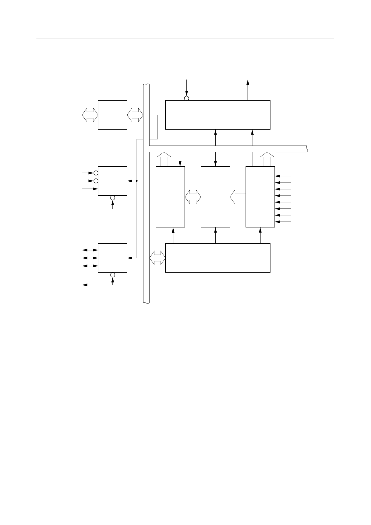
BLOCK DIAGRAM
INTA INT
Data
D
- D
7
0
Bus
Buffer
Control Logic
RD
WR
A
CS
CAS
CAS
CAS
SP/EN
Read/
Write
0
Logic
In-
Service
Register
Priority
Resolver
(ISR)
0
1
2
Cascade
Buffer/
Comparator
Interrupt Mask Register (IMR)
Interrupt
Request
Register
(IRR)
IR
IR
IR
IR
IR
IR
IR
IR
0
1
2
3
4
5
6
7
Internal Bus (8 bits)
MSM82C59A-2 Internal Block Dia
ram
2/28
Page 3
¡ Semiconductor MSM82C59A-2RS/GS/JS
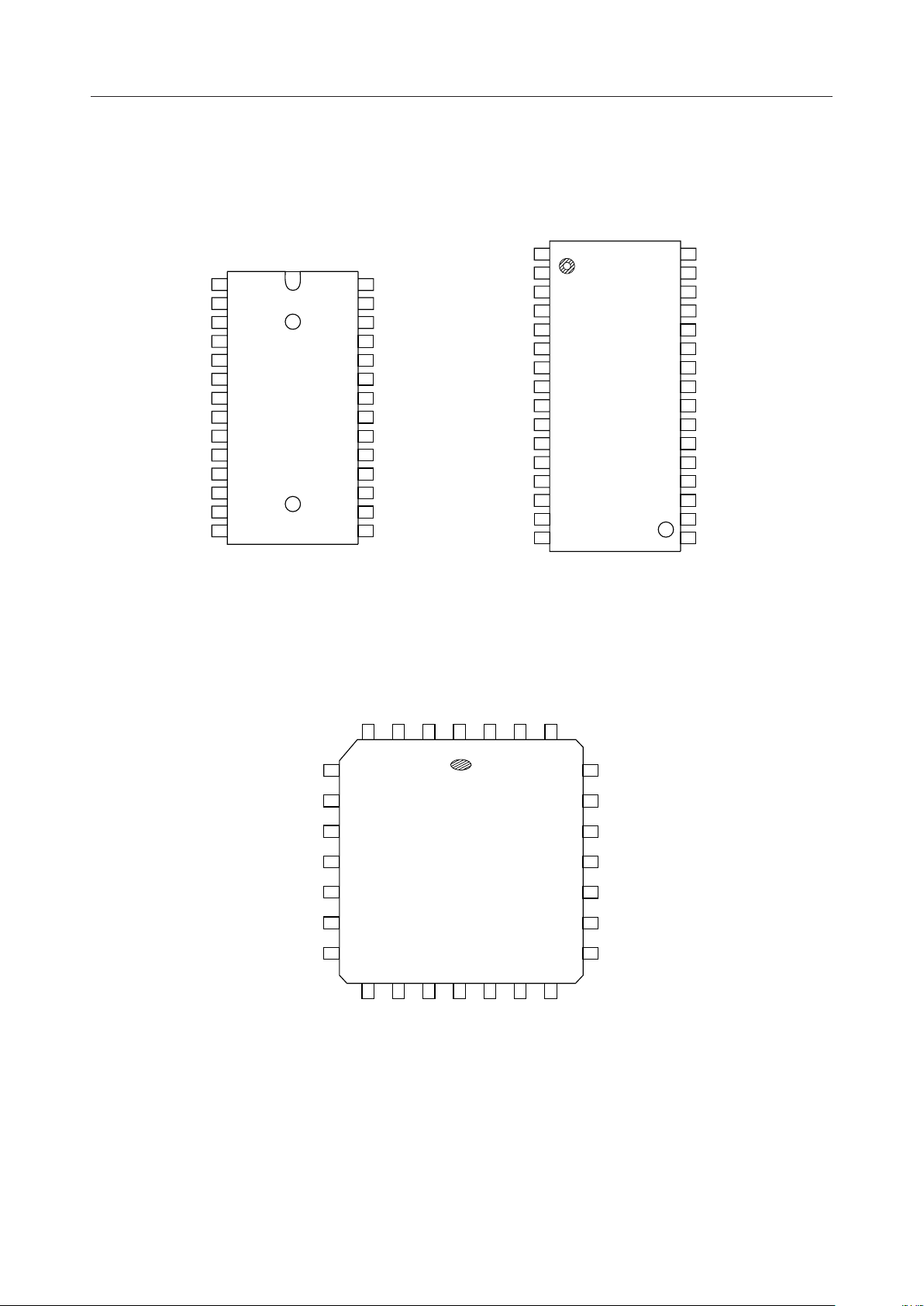
PIN CONFIGURATION (TOP VIEW)
32 pin Plastic SSOP
WR
CAS
CAS
GND
28 pin Plastic DIP
1
CS
2
3
RD
4
D
7
5
D
6
6
D
5
7
D
4
8
D
3
9
D
2
10
D
1
11
D
0
12
0
13
1
14
28
V
CC
27
AO
26
INTA
25
IR
7
24
IR
6
23
IR
5
22
IR
4
21
IR
3
20
IR
2
19
IR
1
18
IR
0
17
INT
16
SP/EN
15
CAS
2
28 pin Plastic QFJ
WR
CAS
CAS
GND
CS
RD
NC
D
D
D
D
D
D
D
D
NC
1
2
3
4
5
7
6
6
7
5
8
4
9
3
10
2
11
1
12
0
13
14
0
15
1
16
32
31
30
29
28
27
26
25
24
23
22
21
20
19
18
17
V
CC
AO
INTA
NC
IR
7
IR
6
IR
5
IR
4
IR
3
IR
2
IR
1
IR
0
NC
INT
SP/EN
CAS
2
7
D
RD3WR2CS1V
4
5
D
6
6
D
5
7
D
4
8
D
3
9
D
2
10
D
1
11
D
0
13
1
CAS
14
GND
12
0
CAS
15
2
CAS
CC
28
16
SP/EN
A027INTA
26
17
18
0
IR
INT
25
24
23
22
21
20
19
IR
7
IR
6
IR
5
IR
4
IR
3
IR
2
IR
1
3/28
Page 4
¡ Semiconductor MSM82C59A-2RS/GS/JS
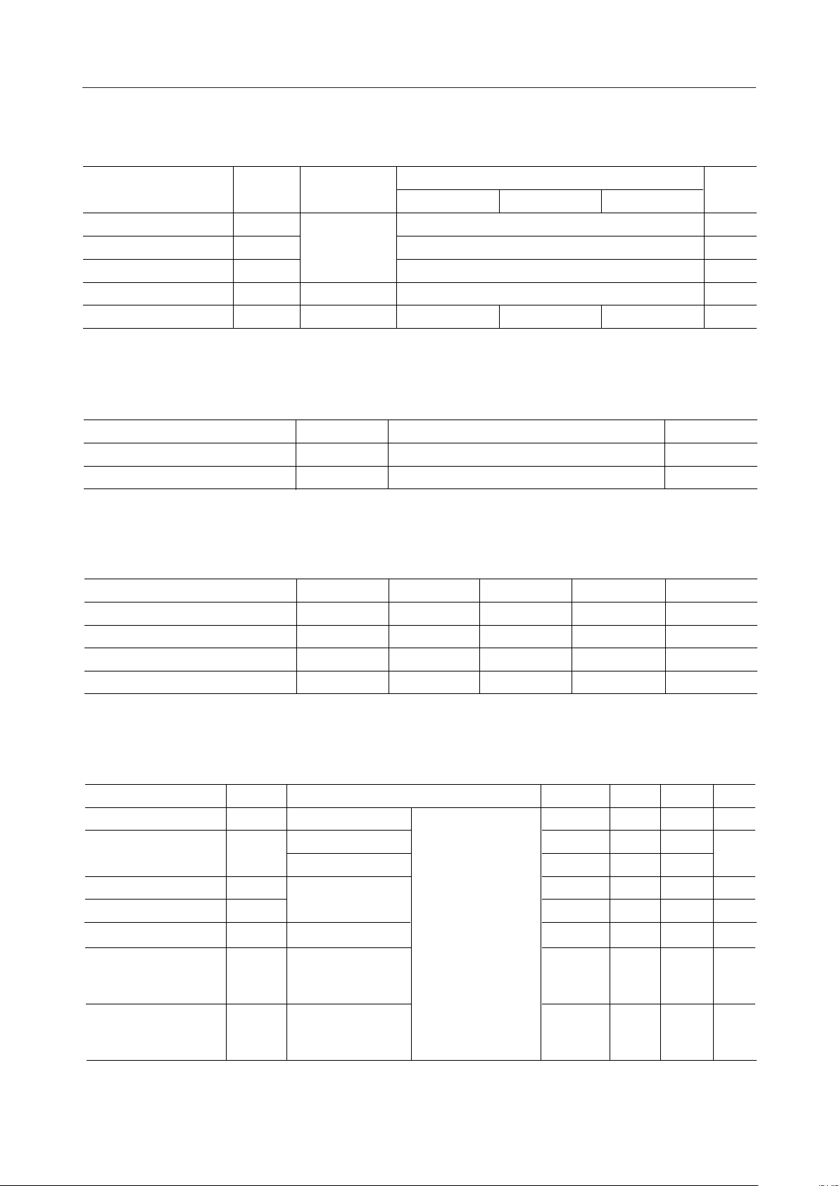
ABSOLUTE MAXIMUM RATINGS
Parameter Unit
Power Supply Voltage
Input Voltage
Output Voltage
Storage Temperature
Power Dissipation
Symbol
V
CC
V
IN
V
OUT
T
STG
P
D
Conditions
Respect
to GND
—
Ta = 25°C
MSM82C59A-2RS
MSM82C59A-2GS MSM82C59A-2JS
–0.5 - +7
–0.5 - V
–0.5 - V
CC
CC
+0.5
+0.5
–55 - +150
0.7
0.90.9
OPERATING RANGES
Rating
Parameter UnitSymbol
Power Supply voltage
Operating Temperature
V
CC
T
OP
Range
3 - 6
–40 - +85
RECOMMENDED OPERATING CONDITIONS
V
V
V
°C
W
V
°C
Parameter UnitSymbol
Power Supply Voltage
Operating Temperature
"L" Lebel Input Voltage V
"H" Lebel Input Voltage
Min.
V
CC
T
OP
IL
V
IH
4.5
-40
-0.5
2.2
Typ.
5V
+25
—
—
Max.
+85
+0.8
V
CC
5.5
+0.5
DC CHARACTERISTICS
Parameter Unit
"L" Level Output Voltage
"H" Level Output Voltage
Input Leak Current
IR Input Leak Current
Output Leak Current
Standby Power Supply
Current
Symbol
V
OL
V
OH
I
LI
I
LIR
I
LO
I
CCS
I
= 2.5 mA
OL
I
= –2.5 mA
OH
I
= –100 mA
OH
0 £ V
0 £ V
CS = V
V
= 0 V, V
IL
IN
OUT
CC,
£ V
£ V
IR = V
IH
Conditions
CC
V
CC
CC
Ta
= –40°C - +85°C
CC
= VCC
= 4.5 V - 5.5 V
Typ. Max.
— 0.4 V
——
——
—1mA
V
Min.
—
3.0
–0.4
CC
–1
–300 — 10
–10
—
—10mA
0.1 100 mA
°C
V
V
V
mA
Average Operation
Power Supply Current
V
= 0 V/VCC
I
CC
IN
C
L
= 0 pF
—
5mA
4/28
Page 5
¡ Semiconductor MSM82C59A-2RS/GS/JS
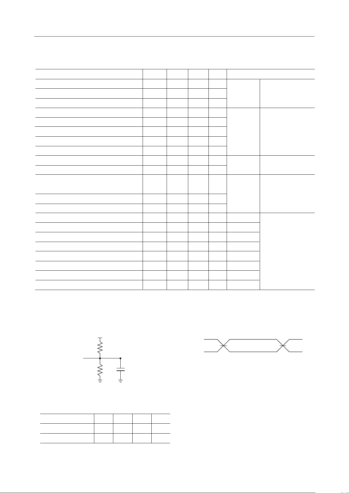
AC CHARACTERISTICS
Parameter
Address Setup Time (to RD)
Address Hold Time (after RD)
RD/INTA Pulse Width
Address Setup Time (to WR)
Address Hold Time (after WR)
WR Pulse Width
Data Setup Time (to WR)
Data Hold Time (after WR)
IR Input Width(Low)
CAS Input Setup Time (to INTA) (Slave)
End of RD to Next RD
End of INTA to Next INTA
End of WR to Next WR
End of Command to Next Command
Data Valid Following RD/ INTA
Data Floating Following RD/ INTA
INT Output Delay Time
CAS Valid Following 1 st. INTA (master)
EN Active Following RD/INTA
EN Inactive Following RD/ INTA
Data Valid after Address
Data Valid after CAS
t
AHRL
t
RHAX
t
RLRH
t
AHWL
t
WHAX
t
WLWH
t
DVWH
t
WHDX
t
JLJH
t
CVIAL
t
RHRL
t
WHWL
t
CHCL
t
RLDV
t
RHDZ
t
JHIH
t
IALCV
t
RLEL
t
RHEH
t
AHDV
t
CVDV
Min. Max.
10
5
160
0
—ns
—ns
—ns
—ns
0—
190
160
0
100
40
160
190
400
—
10
—
—
—
—
—
—
—ns
—ns
—ns
—ns
—ns
—ns
—ns
—ns
120 ns
85 ns
300 ns
360 ns
100 ns
150 ns
200 ns
200 ns
Ta = –40°C - +85°C, V
UnitSymbol
TEST Conditions
—
—
—
—
—
1
2
1
1
1
1
1
1
Read INTA timing
Write timing
INTA sequence
Other timing
Delay times
= 5 V ± 10%
CC
AC Test Circuits
Output from
Device under Test
* Includes Stray and Jig Capacitance
Test Condition Definition Table
Test Condition R2V1
1
2
V1
R1
R2
1.7 V
4.5 V
Test Point
R1
523 W
1.8k W
C1*
1.8k W
Open
A.C. Testing Input, Output Waveform
Input
VIH+0.4 V
1.5V 1.5 V
V
–0.4 V
IL
A. C. Testing: All input signals must switch between
V
–0.4 V and VIH+0.4 V.
IL
T
and TF must be less than of equal to 15 ns.
R
C1
100 pF
30 pF
Output
V
OH
V
OL
5/28
Page 6
¡ Semiconductor MSM82C59A-2RS/GS/JS
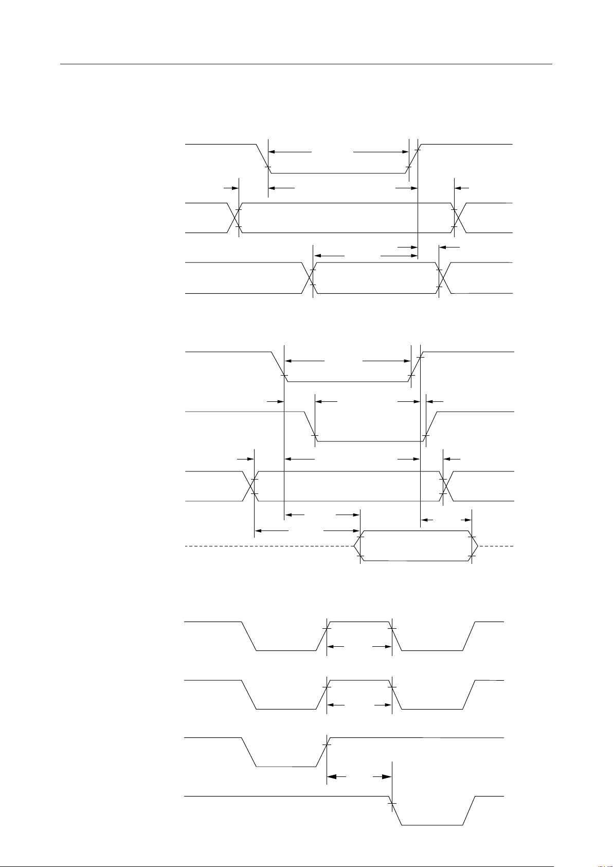
TIMING CHART
Write Timing
WR
t
WLWH
Address Bus
Data Bus
Read/INTA Timing
RD/INTA
Address Bus
Data Bus
CS
A
EN
CS
A
t
AHWL
0
t
DVWH
t
RLRH
t
RLEL
t
AHRL
0
t
RLDV
t
AHDV
t
WHAX
t
RHEH
t
WHDX
t
RHAX
t
RHDZ
Other Timing
RD/INTA/WR
RD/INTA/WR
RD/INTA
WR
t
RHRL
t
WHWL
t
CHCL
6/28
Page 7
¡ Semiconductor MSM82C59A-2RS/GS/JS
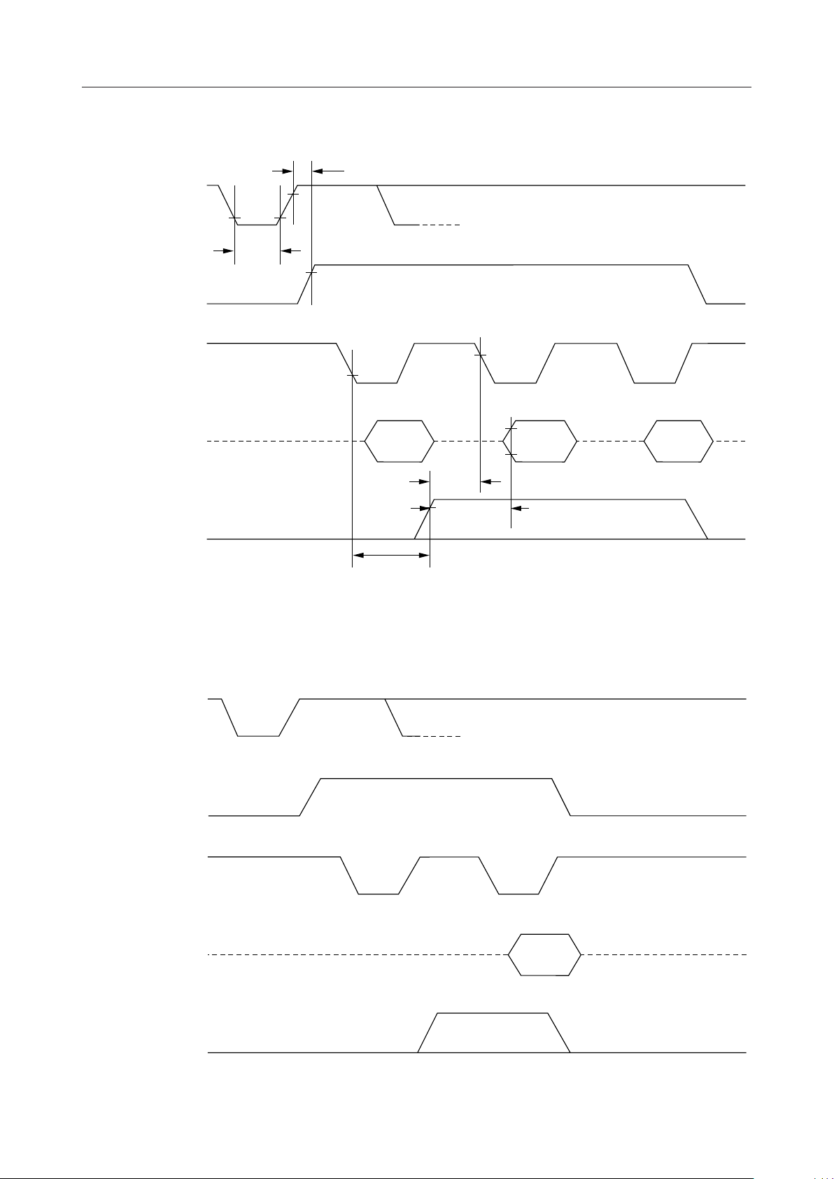
INTA Sequence (85 mode)
t
IR
t
JLJH
INT
INTA
Data Bus
JHIH
t
CVIAL
CAS Address Bus
INTA Sequence (86 mode)
IR
INT
INTA
t
CVDV
t
IALCV
Data Bus
CAS Address Bus
7/28
Page 8

¡ Semiconductor MSM82C59A-2RS/GS/JS
PIN FUNCTION DESCRIPTION
Pin Symbol
D7 - D
0
CS
RD
WR
A
0
Name
Bidirectional
Input/Output
Input/Output
Data Bus
Chip Select
Input
Input
Read Input
Input
Write Input Input
Address
Input
Input
Function
This 3-state 8-bit bidirectional data bus is used in reading status
registers and writing command words through the RD/WR signal
from the CPU, and also in reading the CALL instruction code by the
INTA signal from the CPU.
Data transfer with the CPU is enabled by RD/WR when this pin is at
low level. The data bus (D
thru D7) is switched to high impedance
0
when the pin is at high level. Note that CS does not effect INTA.
Data is transferred from the MSM82C59A-2 to the CPU when this pin
is at low level. IRR (Interrupt Request Register), ISR (In-Service
Register), IMR (Interrupt Mask Register), or a Poll word is selected
by OCW3 and A
.
0
Commands are transferred from the CPU to the MSM82C59A-2 when
this pin is at low level.
This pin is used together with the CS, WR, and RD signals to write
commands in the command registers, and to select and read status
registers. This is normally connected to the least significant bit of the
address bus. (A
for MSM80C85AH, A1 for MSM80C86A-10/88A-10).
0
CAS
SP/EN
INT
INTA
IR
0
-
-
0
2
Cascade
Address
Input/Output
These pins are outputs when the MSM82C59A-2 is used as the
master, and inputs when used as a slave (in cascade mode). These
pins are outputs when in single mode.
Slave Program
Input/Enable
Buffer Output
Interrupt
Output
Interrupt
Acknowledge
Input
Input/Output
Output
Input
This dual function pin is used as an output to enable the data bus
buffer in Buffered mode, and as an input for deciding whether the
MSM82C59A-2 is to be master (SP/EN = 1) or slave (SP/EN =0)
during Non-buffered mode.
When an interrupt request is made to the MSM82C59A-2, the INT
output is switched to high level, and INT interrupt is sent to the CPU.
When this pin is at low level, the CALL instruction code or the
interrupt vector data is enabled onto the data bus. When the CPU
acknowledges the INT interrupt, INTA is sent to the MSM82C59A-2.
(Interrupt acknowledge sequence).
These interrupt request input pins for the MSM82C59A-2 can be set
to edge trigger mode or level trigger mode ( by ICW1). In edge trigger
mode, interrupt request is executed by the rising edge of the IR input
7
Request
Input
Input
and holds it until that input is acknowledged by the CPU. In level
trigger mode, interrupt requests are executed by high level IR inputs
and holds them until that input is acknowledged by the CPU. These
pins have a pull up resistor.
8/28
Page 9
¡ Semiconductor MSM82C59A-2RS/GS/JS
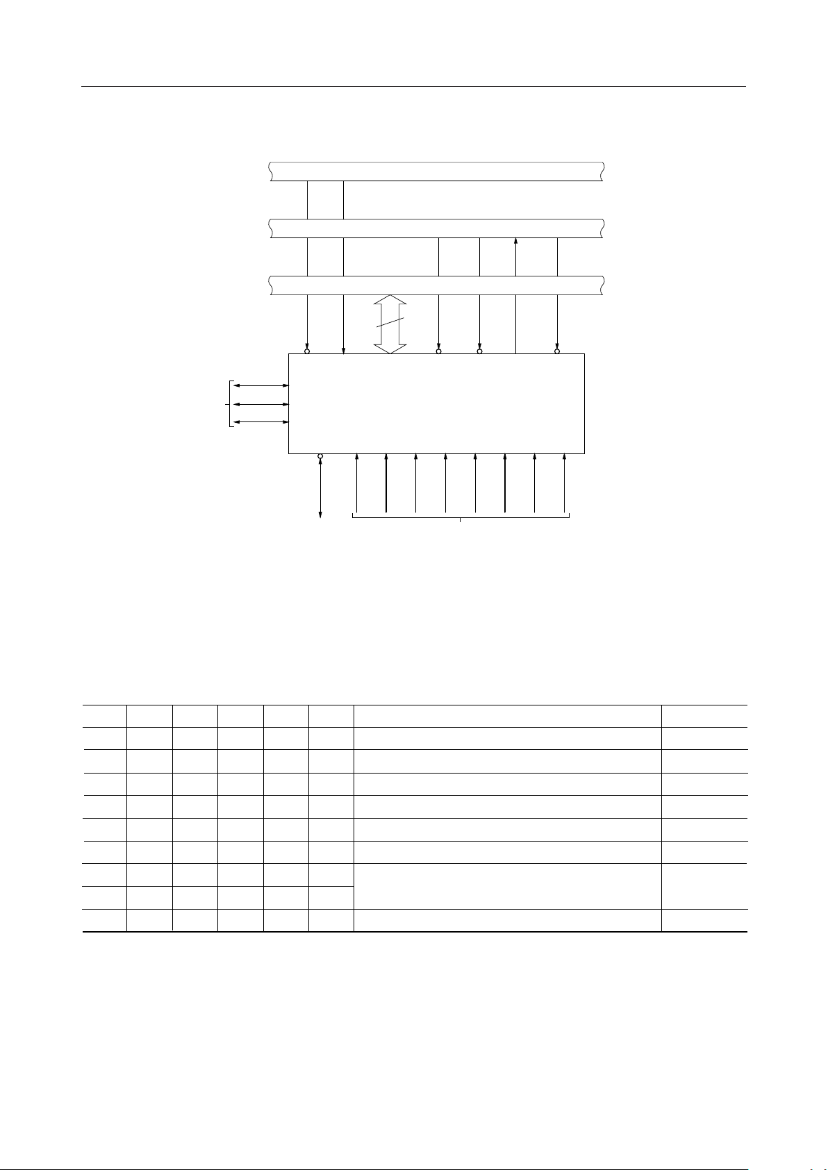
SYSTEM INTERFACE
Address Bus
Control Bus
Data Bus
8 bits
Cascade
Address Bus
A
CS RD INT
CAS
0
CAS
1
CAS
2
D
- D
0
7
0
MSM82C59A-2
SP/EN IR0IR1IR2IR3IR4IR5IR6IR
Slave
Program/Enable
Buffer
Interrupt Requests
WR INTA
7
BASIC OPERATION DESCRIPTION
Data transfers between the 82C59A-2 internal registers and the data bus are listed below.
A
D
0
0
1
¥
¥
0
0
0
1
¥
¥
¥
¥
¥
¥
¥
D
4
0
0
1
RD
3
¥
¥
0
1
¥
¥
¥
¥
¥
WR
0
0
1
1
1
1
1
¥
0
CS
1
1
0
0
0
0
1
¥
0
0
IRR, ISR, or Poll Word Æ Data Bus
0
IMR Æ Data bus
Data Bus Æ OCW2
0
0
Data Bus Æ OCW3
0
Data Bus Æ 1CW1
0
Data Bus Æ OCW1, ICW2, ICW3, ICW4
0
Data Bus Set to High Impedance (when INTA = 1)
1
¥
Combinations Prohibited
Function
Opearation
Read
Read
Write
Write
Write
Write
—
—
9/28
Page 10

¡ Semiconductor MSM82C59A-2RS/GS/JS
OPERATION DESCRIPTION
The MSM82C59A-2 has been designed for real time interrupt driven microcomputer systems.
The MSM82C59A-2 is capable of handling up to 8 levels of interrupt requests, and can be
expanded to cover a maximum of 64 levels when connected to other MSM82C59A-2 devices.
Programming involves the use of system software in the same way as other microcomputer
peripheral I/O devices. Selection of priority mode involves program execution, and enables the
method of requesting interrupts to be processed by the MSM82C59A-2 to be suitably configured
for system requirements. That is, the priority mode can be dynamically updated or reconfigured
during the main program at any time. A complete interrupt structure can be defined as
required, based on the entire system environment.
(1) Functional Description of Each Block
Block Name
IRR, ISR
Priority Resolver
Read/Write Logic
Cascade Buffer Comparator This functional block is involved in the output and comparison of all
IR input line interrupts are processed by a cascaded interrupt request register
(IRR) and the in-service register (ISR). The IRR stores all request levels where
interrupt service is requested, and the ISR stores all interrupt levels being
serviced.
This logic block determines the priority level of the bits set in the IRR. The
highest priority level is selected, and the corresponding ISR bit is set during
INTA pulses.
This block is capable of receiving commands from the CPU. These command
words (ICW) and the operation command words (OCW) store the various
control formats for MSM82C59A-2 operations. This block is also used to
transfer the status of the MSM82C59A-2 to the Data Bus.
MSM82C59A-2 IDs used in the system. These three I/O pins (CAS
are outputs when the MSM82C59A-2 operates as a master, and inputs when it
operates as a slave. When operating as a master, the MSM82C59A-2 sends a
slave ID output to the slave where an interrupt has been applied.
Furthermore, the selected slave sends the preprogrammed subroutine address
onto the data bus during next one or two INTA pulses from the CPU.
Description of Function
0
thru CAS2)
(2) Interrupt Sequence
The major features of the MSM82C59A-2 used in microcomputer systems are the
programmability and the addressing capability of interrupt routines. This latter feature
enables direct or indirect jumping to specific interrupt routines without polling the
interrupt devices. The operational sequence during an interrupt varies for different CPUs.
The procedure for the 85 system (MSM80C85AH) is outlined below.
(i) One or more interrupt requests (IR0 thru IR7) becomes high, and the corresponding IRR
bit is set.
(ii) The MSM82C59A-2 evaluates these requests, and sends an INT signal to the CPU if the
request is judged to be suitable.
(iii) The CPU issues an INTA output pulse upon reception of the INT signal.
(iv) Upon reception of the INTA signal from the CPU, the MSM82C59A-2 releases the
CALL instruction code (11001101) to the 8-bit data bus.
10/28
Page 11

¡ Semiconductor MSM82C59A-2RS/GS/JS
(v) A further two INTA pulses are then sent to the MSM82C59A-2 from the CPU by this
CALL instruction.
(vi) These two INTA pulses result in a preprogrammed subroutine address being sent from
the MSM82C59A-2 to the data bus. The lower 8-bit address is released by the first INTA
pulse, and the higher 8-bit address is released by the second pulse.
The Falling Edge of the second INTA signal sets the ISR bit with the highest priority,
and the Rising Edge of it resets the IRR bit.
(vii) 3-byte CALL instructions are thus released by the MSM82C59A-2. In Automatic End
Of Interrupt (AEOI) mode, the IRS bit is reset at the end of the third INTA pulse. In other
cases, the ISR bit remains set until reception of a suitable EOI command at the end of
the interrupt routine.
The procedure for the 86 system (MSM80C86A-10/88A-10) is identical to the first three
steps of the 85 system. The subsequent steps are described below.
(iv) Upon reception of the INTA signal from the CPU, the ISR bit with the highest priority
is set, and the corresponding IRR bit is reset. In this cycle, the MSM82C59A-2 sets the
data bus to high impedance without driving the Data Bus.
(v) The CPU generates a second INTA output pulse, resulting in an 8-bit pointer to the data
bus by the MSM82C59A-2.
The Falling Edge of the INTA signal sets the ISR bit with the highest priority, and the
Rising Edge of it resets the IRR bit.
(vi) This completes the interrupt cycle. In AEOI mode, the ISR bit is reset at the end of the
second INTA pulse. In other cases, the ISR bit remains set until reception of 3 suitable
EOI command at the end of the interrupt routine.
If the interrupt request is canceled prior to step (iv), that is, before the first INTA pulse has
been received, the MSM82C59A-2 operates as if a level 7 interrupt has been received, and
the vector byte and CAS line operate as if a level 7 interrupt has been requested.
(3) Interrupt Sequence Output
85 Mode (MSM80C85AH)
The sequence in this case consists of three INTA pulses. A CALL operation code is released
to the data bus by the first INTA pulse.
Contents of the First Interrupt Vector Byte
CALL Code
D7 D6 D5 D4 D3 D2 D1 D
1 1 0 0 1 1 0 1
0
The lower address of the interrupt service routine is released to the data bus by the second
INTApulse. If A5-A7 are programmed with an address interval of 4, A0-A4 are automatically
inserted. And if A6 and A7 are programmed at an address interval of 8, A0-A5 are
automatically inserted.
Contents of the second interrupt vector byte
11/28
Page 12

¡ Semiconductor MSM82C59A-2RS/GS/JS
Contents of the Second Interrupt vector byte
IR Interval = 4
D
7
7A
6
5
4
3
2
1
7
A
7
A
7
A
7
A
7
A
7
A
7
A
7
IR Interval = 8
D
7
7A
6
5
4
3
2
1
7
A
7
A
7
A
7
A
7
A
7
A
7
A
7
D
6
A
6
A
6
A
6
A
6
A
6
A
6
A
6
A
6
D
6
A
6
A
6
A
6
A
6
A
6
A
6
A
6
A
6
D
5
A
5
A
5
A
5
A
5
A
5
A
5
A
5
A
5
D
5
D
4
D
3
D
2
D
1
D
0
1110 0
1100 0
1010 0
1000 0
0110 0
0100 0
0010 0
0000 00
D
4
D
3
D
2
D
1
D
0
111000
110000
101000
100000
011000
010000
001000
0000000
The higher address of the interrupt service routine programmed by the second bytes (A8 A15) of the initialization sequence is released to the data bus.
Contents of the Third Interrupt Vector Byte
D7 D6 D5 D4 D3 D2 D1 D
A
15
A
A
14
13
A
A
12
11
A
10
A
9
0
A
8
86 Mode (MSM80C86A-10/88A-10)
Apart from the two interrupt acknowledge cycles and the absence of a CALL operation
code, the 86 mode is the same as the 85 mode. The first INTA cycle freezes interrupt status
to resolve the priority internally in the same way as in 85 mode. When the device is used
as a master, an interrupt code is issued to the cascade line at the end of the INTA pulse.
During this first cycle, the data bus buffer is kept at high impedance without any data to
the CPU. During the second INTA cycle, the MSM82C59A-2 sends a byte of interrupt code
to the CPU. Note that in 86 mode, the Address Interval (ADI) control status is ignored and
A5-A10 is not used.
12/28
Page 13

¡ Semiconductor MSM82C59A-2RS/GS/JS
Contents of Interrupt Vector Byte in 86 System Mode
IR
IR
IR
IR
IR
IR
IR
D
7
7
6
5
4
3
2
1
0
T
7
T
7
T
7
T
7
T
7
T
7
T
7
T
7
D
6
T
6
T
6
T
6
T
6
T
6
T
6
T
6
T
6
D
5
T
5
T
5
T
5
T
5
T
5
T
5
T
5
T
5
D
4
T
4
T
4
T
4
T
4
T
4
T
4
T
4
T
4
D
3
T
3
T
3
T
3
T
3
T
3
T
3
T
3
T
3
D
2
D
111
110
101
100
011
010
001
000IR
(4) Programming the MSM82C59A-2
The MSM82C59A-2 receives two types of command words generated by the CPU.
(i) Initialization Command Words (ICW1 thru ICW4)
Before commencing normal operations, each MSM82C59A-2 in the system must be
initialized by two to four WR pulse sequence.
ICW1
1
D
0
No (SNGL = 1)
No (IC4 = 0)
ICW2
In
Cascade
Mode?
Yes (SNGL = 0)
ICW3
Is
ICW4
needed?
Yes (IC4 = 1)
ICW4
Interrupt request
reception preparations
completed
Initialization Sequence
13/28
Page 14

¡ Semiconductor MSM82C59A-2RS/GS/JS
(ii) Operation Command Words (OCW1 thru OCW3)
These commands are used in operating the MSM82C59A-2 in the following modes.
a. Fully Nested Mode
b. Rotating Priority Mode
c. Special Mask Mode
d. Polled Mode
The OCW can be written into the MSM82C59A-2 any time after initialization has been
completed.
(5) Initialization Command Words (ICW1 thru ICW4)
When a command is issued with D4 = 1 and A0 = 0, it is always regarded as an Initialization
Command Word 1 (ICW1). Starting of the initialization sequence by ICW1 results in
automatic execution of the following steps.
a. The edge sense circuit is reset, and a low to high transition is necessary to generate an
interrupt.
b. The interrupt mask register is cleared.
c. The IR7 input is assigned priority 7 (lowest priority)
d. Slave mode address is set to 7.
e. The Special Mask Mode is cleared, and the Status Read is set to IRR.
f. All ICW4 functions are cleared if IC4 = 0, resulting in a change to Non-Buffered mode, no-
Auto EOI, and 85 mode.
Note: Master/slave in ICW4 can only be used in buffered mode.
(i) Initialization Command Words 1 and 2 (ICW1 and ICW2)
A4 thru A15: (Starting address of interrupt service routines)
In 85 mode, 8 request levels CALL 8 locations at equivalent intervals in
the memory. The memory location interval can be set at this stage to 4 or
8 by program. (ÆADI)Hence, either 32 or 64 bytes/page respectively are
used in the 8 routines.
The address format is 2 bytes long (A0 thru A15). When the routine
interval is 4, A0 thru A4 are inserted automatically by the MSM82C59A2, and A5 thru A15 are programmed externally. When the interval is 8,
on the other hand, A0 thru A5 are inserted automatically by the
MSM82C59A-2, and A6 thru A15 are programmed externally. In 86
mode, T3 thru T7 are inserted in the 5 most significant bits of the vector
type. And the MSM82C59A-2 sets the 3 least significant bits according to
the interrupt level. A0 thru A10 are ignored, and the ADI (address
interval) has no effect.
LTIM: The MSM82C59A-2 is operated in level triggered mode when LTIM = 1,
and the interrupt input edge circuit becomes disabled.
ADI: Designation of the CALL address interval. Interval = 4 when ADI = 1,
and interval = 8 when ADI = 0.
SNGL: SNGL = 1 indicates the existence of only one MSM82C59A-2 in the
system. ICW3 is not required when SNGL = 1.
IC4: ICW4 is required when this bit is set, but not required when IC4 = 0.
14/28
Page 15

¡ Semiconductor MSM82C59A-2RS/GS/JS
(ii) Initialization Command Word 3 (ICW3)
This command word is written when there is more than one MSM82C59A-2 used in
cascade connections in the system, and is loaded into an 8-bit slave register. The
functions of this slave register are listed below.
a. In a master mode system (BUF = 1 and M/ S = 1 in ICW4 or SP/EN = 1). “1” is set
in each bit where a slave has been connected.
In 85 mode, the master MSM82C59A-2 releases byte 1 of the CALL sequence to
enable the corresponding slave to release byte 2 or 3 (only byte 2 in 86 mode) through
the cascade line.
b. In slave mode (BUF = 1 and M/S = 0 in ICW4 or SP/EN = 0). Bits 0 thru 2 identify
the slave. The slave compares these bits with the cascade input, and releases bytes
2 and 3 of the CALL sequence (only byte 2 in 86 mode) if a matching result is obtained.
(iii) Initialization Command Word 4 (ICW4)
SFNM: Special Fully Nested Mode is programmed when SFNM = 1.
BUF: Buffered mode is programmed when BUF = 1. In Buffered mode, SP/EN is an
output, and Master/slave is selected by the M/S bit.
M/S: If buffered mode is selected, the MSM82C59A-2 is programmed as the master
when M/S = 1, and as a slave when M/S = 0. M/S is ignored, however, when
BUF = 0.
AEOI: Automatic End Of Interrupt mode is programmed by AEOI = 1.
mPM: (Microprocessor mode)
The MSM82C59A-2 is set to 85 system operation when mPM = 0, and to 86
system operation when mPM = 1.
15/28
Page 16

¡ Semiconductor MSM82C59A-2RS/GS/JS
)
ICW1
ICW2
ICW3
(Master)
A
0 A
A
D
0
D
0
D
7
A
7
D
7
D
6
A
6
D
6
D
5
5
5
4
1 LTIM ADI SNGL IC4
D
4
1 A15/T7A14/T6A13/T5A12/T4A11/T
A
1 S
D
0
D
7
S
7
D
6
S
6
D
5
5
4
S
4
D
D
3
D
2
D
1
0
1: ICW4 required
0: ICW4 not required
1: Single
0: Cascade
CALL address interval
1: Interval = 4
0: Interval = 8
1: Level triggered mode
0: Edge triggered mode
Interrupt vector address
thru A
A
5
(Valid only in 85 mode)
D
D
3
A
3
D
2
A
10
D
1
9
0
A
8
7
Interrupt vector address
thru A15 (85 mode)
A
8
Interrupt vector address
thru T7 (86 mode)
T
3
D
S
D
3
S
3
D
2
S
2
D
1
1
0
S
0
ICW3
(Slave)
ICW4
A
1 0 0 0 0 0 ID
D
0
D
7
D
6
D
5
D
4
D
3
D
2
ID
2
D
1
ID
1
NOTE: Slave ID indicates the IR input
A
D
0
D
7
D
6
D
5
D
4
D
3
D
2
D
1
1 0 0 0 SFNM BUF M/S AEOI mPM
0 ¥
1 0
1 1
Non-buffered mode
Buffered mode (slave)
Buffered mode (master)
1: IR input holds slave
0: IR input does not hold slave
0
0
Slave ID
0
1
2
3
0
1
0
1
0
0
1
1
0
0
0
0
of the corresponding master.
0
1: 86 mode
0: 85 mode
1: Automatic EOI mode
0: Normal EOI mode
NOTE:
4
5
0
1
0
0
1
1
¥ den 0 tes
not specified
6
7
0
1
1
1
1
1
1: Special fully nested mode
0: Not special fully nested mode
Initialization Command Words (ICW1 thru ICW4
16/28
Page 17

¡ Semiconductor MSM82C59A-2RS/GS/JS
(6) Operation Command Words (OCW1 thru OCW3)
When Initialization Command Words (ICWs) are programmed in the MSM82C59A-2, the
interrupt input line is ready to receive interrupt requests. The Operation Command Words
(OCWs) enable the MSM82C59A-2 to be operated in various modes while the device is in
operation.
(i) Operation Command Word 1 (OCW1)
OCW1 sets and resets the mask bits of the Interrupt Mask Register (IMR). M0 thru M7
represent 8 mask bits. The channel is masked when M = 1, but is enabled when M = 0.
(ii) Operation Command Word 2 (OCW2)
R, SL, EOI: The Priority Rotation and End of Interrupt mode plus combinations of the
two are controlled by combinations of these 3 bits. These combinations are
listed in the operation command word format table.
L2, L1, L0: These bits indicate the specified interrupt level when SL = 1.
(iii) Operation Command Word 3 (OCW3)
ESMM: This enables the Special Mask Mode. The special mask mode can be set and
reset by the SMM bit when ESMM = 1. The SMM bit is ignored when ESMM
= 0.
SMM: (Special Mask Mode)
The MSM82C59A-2 is set to Special Mask Mode when ESMM = 1 and SMM =
1, and is returned to normal mask mode when ESMM = 1 and SMM = 0. SMM
is ignored when ESMM = 0.
17/28
Page 18

¡ Semiconductor MSM82C59A-2RS/GS/JS
OCW1
OCW2
A
D
0
D
7
D
6
D
5
D
4
D
3
D
2
1
1 M7 M6 M5 M4 M3 M2 M1 M0
A
D
0
D
7
D
6
D
5
D
4
D
3
D
2
1
0 R SL EOI 0 0 L2 L1 L0
0 0 1
0 1 1
1 0 1
1 0 0
0 0 0
1 1 1
1 1 0
0 1 0
Non-specific EOI command
Specific EOI command (NOTE)
Rotate on non-specific EOI command
Rotate in automatic EOI mode (SET)
Rotate in automatic EOI mode (Clear)
Rotate on specific EOI command (NOTE)
Set priority comand (NOTE)
No operation
D
0
Intterupt Mask
1: Mask set
0: Mask reset
D
0
Active IR Level
0
1
2
3
4
5
6
7
0
1
0
1
0
1
0
1
0
0
1
1
0
0
1
1
0
0
0
0
1
1
1
1
End of interrupt
Automatic rotation
Specific rotation
OCW3
NOTE: L0 thru L2 used
A
D
0
D
7
D
6
D
5
D
4
D
3
D
2
1
0 0 ESMM SMM 0 1 P RR RIS
Operation Command Words (OCW1 thru OCW3)
D
0
Read Register Command
0 1 0
0 0 1
No operation
Polling
1: Poll command
0: No-poll command
Special Mask Mode
0 1 0
0 0 1
No operation
Read
IRR by
next RD
Reset
special
mask
mode
1
1
Read
ISR by
next RD
1
1
Set
special
mask
mode
18/28
Page 19

¡ Semiconductor MSM82C59A-2RS/GS/JS
(7) Fully Nested Mode
As long as the MSM82C59A-2 has not been programmed to another mode, this Fully
Nested mode is set automatically after initialization. The interrupt requests are ordered
in priority sequentially from 0 to 7 (where 0 represents highest priority). If an interrupt is
then requested and is acknowledged highest priority, a corresponding vector address is
released, and the corresponding bit in the in-service register (ISR) is set. The IS bit remains
set until an End of Interrupt (EOI) command is issued from the microprocessor before
returning from the interrupt service routine, or until the rising edge of the last INTA pulse
arrives when the AEOI bit has been set.
When the IS bit is set, interrupts of the same or lower priority are inhibited - only interrupts
of higher priority can be generated. In this case, interrupts can be acknowledged only
when the internal interrupt enable F/F in the microprocessor has been enabled again
through software. Following the initialization sequence, IR0 has the highest priority, and
IR7 has the lowest. This priority can be changed by rotating priority mode in OCW2.
(8) End of Interrupt (EOI)
When the AEOI bit in ICW4 is set, the in-service (IS) bit is automatically reset by the rising
edge of the last INTA pulse, or else is reset only when an EOI command is issued to the
MSM82C59A-2 prior to returning from the interrupt service routine.
And in cascade mode, the EOI command must be issued twice - once for the master, and
once for the corresponding slave.
EOI commands are classified into specific EOI commands and Non-Specific EOI commands.
When the MSM82C59A-2 is operated in Fully Nested mode, the IS bit to be reset can be
determined on EOI. If the Non-Specific EOI command is issued, the highest IS bit of those
that are set is reset automatically, because the highest IS level is always the last servicing
level in the Fully Nested mode, the MSM82C59A-2 will no longer be able to determine the
last acknowledged level. In this case, it will be necessary to issue a Specific EOI which
includes the IS level to be reset as part of the command. When the MSM82C59A-2 is in
Special Mask mode, care must be taken to ensure that IS bits masked by the IMR bit can
not reset by the Non-Specific EOI.
(9) Automatic End of Interrupt (AEOI) Mode
When AEOI = 1 in ICW4, the MSM82C59A-2 continues to operate in AEOI mode until
programmed again by ICW4. In this mode, the MSM82C59A-2 automatically performs
Non-Specific EOI operation at the rising edge of the last INTA pulse (the third pulse in 85
systems, and the second pulse in 86 systems). In terms of systems, this mode is best used
in nested multiple level interrupt configurations. It is not necessary when there is only one
MSM82C59A-2. AEOI mode is only used in a master MSM82C59A-2 device, not in a slave.
(10) Automatic Rotation (Devices with Equal Priority)
In some applications, there is often a number of devices with equal priority. In this mode,
the device where an interrupt service has just been completed is set to the lowest priority.
At worst, therefore, a particular interrupt request device may have to wait for seven other
devices to be serviced at least once each. There are two methods for Automatic Rotation
using OCW2 - Rotation on Non-Specific EOI command, and Rotation in Automatic EOI
mode.
19/28
Page 20

¡ Semiconductor MSM82C59A-2RS/GS/JS
Before Rotation
(IR4 the highest priority requesting service)
IS7 IS6 IS5 IS4 IS3 IS2 IS1 IS0
IS Status
0 1 0 1 0 0 0 0
Priority Status
After Rotation
(IR4 was serviced, all other priorities rotated correspondingly)
IS Status
Priority Status
7 6 5 4 3 2 1 0
Lowest Highest
IS7 IS6 IS5 IS4 IS3 IS2 IS1 IS0
0 1 0 0 0 0 0 0
2 1 0 7 6 5 4 3
Highest
Lowest
(11) Specific Rotation (Specific Priority)
All priority levels can be changed by programming the lowest priority level (Set Priority
Command in OCW2). For example, if IR5 is programmed as the device of lowest priority,
IR6 will have the highest priority. In this mode, the internal status can be updated during
OCW2 by software control. This is unrelated, however, to the EOI command in the same
OCW2.
Priority level can also be changed by using the OCW2 Rotate On Specific EOI command.
(12) Interrupt Mask
Interrupt inputs can be masked individually by Interrupt Mask Registers (IMR)
programmed through the OCW1. Each interrupt channel is masked (disabled) when the
respective IMR bit is set to “1”. IR0 is masked by bit 0, and IR1 is masked by bit 1. Masking
of any particular channel has no effect on other channels.
20/28
Page 21

¡ Semiconductor MSM82C59A-2RS/GS/JS
(13) Special Mask Mode
In some applications, there is a need for dynamic updating of the system’s priority level
structure by software control during execution of an interrupt service routine. For
example, it may be necessary to inhibit the lower priority requests for part of the execution
of a certain routine while enabling for another part. In this case, it is difficult to enable all
lower priority requests if the IS bit has not yet been reset by the EOI command after an
interrupt request has been acknowledge (during execution of a service routine). All of
these requests would normally be disabled.
Hence the use of the Special Mask mode. When a mask bit is set by OCW1 in this mode,
the corresponding interrupt level requests are disabled. And all other unmasked level
requests (at both higher and lower priority levels) are enabled. Interrupts can thus be
enabled selectively by loading the mask register.
In this mode, the specific EOI Command should be used.
This Special Mask mode is set by OCW3 ESMM = 1 and SMM = 1, and reset by ESMM =
1 and SMM = 0.
(14) POLL Command
In this mode, the INT output is not used, the internal interrupt enable F/F of the
microprocessor is reset, and interrupt inputs are disabled. Servicing the I/O device is
executed by software using the Poll command.
The Poll command is issued by setting P in OCW3 to “1”. The MSM82C59A-2 regards the
next RD pulse as reception of an interrupt, and if there is a request, the corresponding IS
bit is set and the priority level is read out. Interrupts are frozen between WR and RD.
D7D6D5D4D3D2D1D
1 0 0 0 0 W2 W1 W0Poll Word
W0 thru W2:1:Binary coded highest priority level of service
being requested.
Set to "1" when there is an interrupt.
0
This mode is useful when there is a command routine for a number of levels, and the INTA
sequence is not required. ROM space can thus be saved.
21/28
Page 22

¡ Semiconductor MSM82C59A-2RS/GS/JS
(15) Reading MSM82C59A-2 Status
The status of a number of internal registers can be read out for updating user information
on the system. The following registers can be read by means of OCW3 (IRR and ISR) and
OCW1 (IMR).
a. IRR: (Interrupt Request Register) 8-bit register for storing interrupt requesting levels.
b. ISR: (In-Service Register) 8-bit register for storing priority levels being serviced.
c. IMR: (Interrupt Mask Register) 8-bit register for storing interrupt request lines to be
masked.
The IRR can be read when a Read Register Command is issued with OCW3 (RR = 1 and
RIS = 0) prior to the RD pulse, and the ISR can be read when a Read Register command is
issued with OCW3 (RR = 1 and RIS = 1) prior to the RD pulse. And as long as the read status
does not change, OCW3 is not required each time before the status is read. This is because
the MSM82C59A-2 remembers whether IRR or ISR was selected by the previous OCW3.
But this is not true when poll is used.
The MSM82C59A-2 is set to IRR after initialization. OCW3 is not required to read IMR.
IMR is issued to the data bus if RD = 0 and A0 = 1 (OCW1).
Reading status is disabled by polling when P = 1 and RR = 1 in OCW3.
(16) Edge and Level Trigger Mode
This mode is programmed by using bit 3 (LTIM) in ICW1. When LTIM = 0, the interrupt
request is recognized by the IR input transition from Low to High. As long as the IR input
is kept at High, no other interrupt is generated. Since interrupt requests are recognized
by the IR input “H” level when LTIM = 1, edge detection is not required.
The interrupt request must be cancelled before output of the EOI command, and before the
interrupt is enabled in order to prevent the generation of a second interrupt by the CPU.
The IR input must be held at High level until the falling edge of the first INTA pulse,
irrespective of whether edge sense or level sense is employed. If the IR input is switched
to Low level before the first INTA pulse, the default IR7 is generated when the interrupt
is acknowledged by the CPU. This can be an effective safeguard to be adopted to detect
interrupts generated by the noise glitches on the IR inputs. To take advantage of this
feature, the IR7 routine is used as a “clean up” routine where the routine is simply
executing a return instruction and the interrupt is subsequently ignored. When the IR7 is
required for other purposes, the default IR7 can be detected by reading the ISR. Although
correct IR7 interrupts involve setting of the corresponding ISR bit, the default IR7 is not
set.
IR7 routine
No
(IR noise
detection)
IS7=1?
Yes
IR7 service
processing
EOI
RETURN
22/28
Page 23

¡ Semiconductor MSM82C59A-2RS/GS/JS
(17) Special Fully Nested Mode
This mode is used in large systems where the cascade mode is used and the respective
Interrupt Requests within each slave have to be given priority levels. In this case, the
Special Fully Nested mode is programmed to the master by using ICW4. This mode is
practically identical to the normal Fully Nested mode, but differs in the following two
respects.
a. When an interrupt request is received from a particular slave during servicing, a new
interrupt request from an IR with a higher priority level than the interrupt level of the
slave being serviced is recognized by the master and the interrupt is applied to the
processor without the master priority logic being inhibited by the slave. In normal
Fully Nested mode, if the request is in service, a slave is masked and no other requests
can be recognized from the same slave.
b. When exiting from an interrupt service routine, it is first necessary to check whether
or not the interrupt which has just been serviced by soft ware was the only interrupt
from that slave. This is done by sending a Non-Specific EOI command to that slave,
followed by reading of the In-Service Register (ISR) to see whether that register has
become all ‘0’. A Non-Specific EOI is sent to the master too if the ISR is empty, and if
not no EOI should be sent.
(18) Buffered Mode
Control for buffer enabling is required when the MSM82C59A-2 is used in a large system
where a data bus drive buffer is needed and cascade mode is used. When buffered mode
is selected, the MSM82C59A-2 sends an enable signal on the SP/EN pin to enable the
buffer. In this mode, the SP/EN output always becomes active while the MSM82C59A2’s data bus output is enabled. Therefore, the MSM82C59A-2 requires programming to
enable it to distinguish master from slave. Buffered mode is programmed by bit 3 in ICW4,
and the ability to distinguish master from slave is programmed by bit 2 in ICW4.
(19) Cascade Mode
To enable the MSM82C59A-2 to handle up to 64 priority levels, a maximum of 8 slaves can
be easily connected to one master device.
The master controls the slaves through three cascade lines, the cascade bus executes like
a slave chip select during the INTA sequence.
In cascade configuration, slave interrupt outputs (INT) are connected to master interrupt
request inputs (IR). When a slave IR becomes active and is acknowledged, the master
enables the corresponding slave to release the routine address for that device during bytes
2 and 3 (only byte 2 in 86 mode) of the INTA sequence.
The cascade bus line is normally kept at low level, and holds the slave address during the
period from the rising edge of the first INTA pulse up to the rising edge of the thirdINTA
pulse (or the second INTA pulse in 86 mode).
Each MSM82C59A-2 device in the system can operate in different modes in accordance
with their initialization sequences. EOI commands must be issued twice, once for the
master once for the corresponding slave. Each MSM82C59A-2 requires an address
decoder to activate the respective chip select (CS) inputs.
Since the cascade line is normally kept at low level, note that slaves must be connected to
the master IR0 only after all slaves have been connected to the other IRs.
23/28
Page 24

¡ Semiconductor MSM82C59A-2RS/GS/JS
Address Bus
Control Bus
Data Bus
Cascade Bus
A
CS
0D0
MSM82C59A-2
SP/EN
GND
(Slave)
76543210
76543210
- 7INTA
CAS
A
-
0
INT
CS
2
SP/EN
GND
- 7INTA
0D0
MSM82C59A-2
(Slave)
76543210
76543210 7 54 210
Interrupt Requests
MSM82C59A-2 Cascade Connections
CAS
0
INT
A
CS
-
2
CAS0 -
SP/EN
M7 M6 M5M4M3 M2 M1M0
V
CC
- 7INTA
0D0
2
MSM82C59A-2
(Master)
INT
24/28
Page 25

¡ Semiconductor MSM82C59A-2RS/GS/JS
g
g
g
Precautions for operation
Contents: In the case of a cascade edge trigger, the low level width (TILIH) of a slave INT signal
may be less than the low level width (TJLJH:100 ns min.) of a master IR input signal.
This occurs when an interruption request with high order priority is provided to the
slave unit before the INTA cycle ends. Fig.1 shows a system configuration, Fig.2 a bug
operation timing chart, and Fig.3 a normal operation timing chart. TILIH is not
specified.
CPU
INTR
INTm
MSM82C59A-2
Master
INT
INTs
MSM82C59A-2
Slave
IR
1
IR
2
INT
IR1s
IR2s
INT
IR
2S
IR
1S
INTA
(IR7m)
S
INTm
INTA
INTA
. 1 System Configuration
Fi
Fi
. 2 Bug Operation Timing Chart
IR
7
IR7m
INTA
TILIH (TJLJH) does not satisfy
the spec.
INT
is not accepted.
S
INT
IR
2S
IR
1S
INTA
(IR7m)
S
INTm
TILIH
(TJLJH)
. 3 Normal Operation Timing Chart
Fi
25/28
Page 26

¡ Semiconductor MSM82C59A-2RS/GS/JS
PACKAGE DIMENSIONS
(Unit : mm)
DIP28-P-600-2.54
Package material
Lead frame material
Pin treatment
Solder plate thickness
Package weight (g)
Epoxy resin
42 alloy
Solder plating
5 mm or more
4.30 TYP.
Notes for Mounting the Surface Mount Type Package
The SOP, QFP, TSOP, SOJ, QFJ (PLCC), SHP and BGA are surface mount type packages, which
are very susceptible to heat in reflow mounting and humidity absorbed in storage.
Therefore, before you perform reflow mounting, contact Oki’s responsible sales person for the
product name, package name, pin number, package code and desired mounting conditions
(reflow method, temperature and times).
26/28
Page 27

¡ Semiconductor MSM82C59A-2RS/GS/JS
(Unit : mm)
QFJ28-P-S450-1.27
Spherical surface
Package material
Lead frame material
Pin treatment
Solder plate thickness
Package weight (g)
Epoxy resin
Cu alloy
Solder plating
5 mm or more
1.00 TYP.
Notes for Mounting the Surface Mount Type Package
The SOP, QFP, TSOP, SOJ, QFJ (PLCC), SHP and BGA are surface mount type packages, which
are very susceptible to heat in reflow mounting and humidity absorbed in storage.
Therefore, before you perform reflow mounting, contact Oki’s responsible sales person for the
product name, package name, pin number, package code and desired mounting conditions
(reflow method, temperature and times).
27/28
Page 28

¡ Semiconductor MSM82C59A-2RS/GS/JS
(Unit : mm)
SSOP32-P-430-1.00-K
Mirror finish
Package material
Lead frame material
Pin treatment
Solder plate thickness
Package weight (g)
Epoxy resin
42 alloy
Solder plating
5 mm or more
0.60 TYP.
Notes for Mounting the Surface Mount Type Package
The SOP, QFP, TSOP, SOJ, QFJ (PLCC), SHP and BGA are surface mount type packages, which
are very susceptible to heat in reflow mounting and humidity absorbed in storage.
Therefore, before you perform reflow mounting, contact Oki’s responsible sales person for the
product name, package name, pin number, package code and desired mounting conditions
(reflow method, temperature and times).
28/28
 Loading...