


E2O0020-27-X3
¡ Semiconductor MSM82C55A-2RS/GS/VJS
¡ Semiconductor
This version: Jan. 1998
Previous version: Aug. 1996
MSM82C55A-2RS/GS/VJS
CMOS PROGRAMMABLE PERIPHERAL INTERFACE
GENERAL DESCRIPTION
The MSM82C55A-2 is a programmable universal I/O interface device which operates as high
speed and on low power consumption due to 3m silicon gate CMOS technology. It is the best
fit as an I/O port in a system which employs the 8-bit parallel processing MSM80C85AH CPU.
This device has 24-bit I/O pins equivalent to three 8-bit I/O ports and all inputs/outputs are
TTL interface compatible.
FEATURES
• High speed and low power consumption due to 3m silicon gate CMOS technology
• 3 V to 6 V single power supply
• Full static operation
• Programmable 24-bit I/O ports
• Bidirectional bus operation (Port A)
• Bit set/reset function (Port C)
• TTL compatible
• Compatible with 8255A-5
• 40-pin Plastic DIP (DIP40-P-600-2.54): (Product name: MSM82C55A-2RS)
• 44-pin Plastic QFJ (QFJ44-P-S650-1.27): (Product name: MSM82C55A-2VJS)
• 44-pin Plastic QFP (QFP44-P-910-0.80-2K): (Product name: MSM82C55A-2GS-2K)
1/26
¡ Semiconductor MSM82C55A-2RS/GS/VJS
CIRCUIT CONFIGURATION
V
GND
D
- D
0
RD
WR
RESET
CS
8
CC
8
Group A
Port A
8
PA
- PA
0
7
(8)
8
Group A
Control
4
(High Order
Group A
Port C
4
PC4 - PC
7
4 Bits)
8
7
Data
Bus
Buffer
8
Internal Bus Line
8
4
(Low Order
Group B
Port C
4 Bits)
4
PC0 - PC
3
Group B
Read/
Write
Control
Logic
Control
8
Group B
Port B
8
PB0 - PB
7
(8)
A
0
A
1
2/26
¡ Semiconductor MSM82C55A-2RS/GS/VJS
PIN CONFIGURATION (TOP VIEW)
40 pin Plastic DIP
CS
GND
A
A
PC
PC
PC
PC
PC
PC
PC
1
PA
3
2
PA
2
3
PA
1
4
PA
0
5
RD
6
CS
7
GND
8
A
1
9
A
0
10
PC
7
11
PC
6
12
PC
5
13
PC
4
14
PC
0
15
PC
44 pin Plastic QFP
0PA1PA2PA3
RD
PA
4443424140
1
2
3
1
4
0
5
7
6
6
7
5
8
4
9
0
10
1
11
2
1415161718
12
13
3PB0PB1PB2
NC
PC
VCCPA
39
38
CC
V
PB
4
5PA6PA7
PA
37
192021
3
4PB5PB6
PB
363534
WR
22
NC
33
32
31
30
29
28
27
26
25
24
23
RESET
D
0
D
1
D
2.
D
3
D
4
D
5
D
6
D
7
V
CC
PB
7
1
16
PC
2
17
PC
3
18
PB
0
19
PB
1
20
PB
2
44 pin Plastic QFJ
0PA1PA2PA3
RD
PA
6
5
432
NC
1
4
PA
44
5PA6PA7
PA
43
424140
40
39
38
37
36
35
34
33
32
31
30
29
28
27
26
25
24
23
22
21
PA
PA
PA
PA
WR
RESET
D
0
D
1
D
2
D
3
D
4
D
5
D
6
D
7
V
CC
PB
PB
PB
PB
PB
WR
4
5
6
7
7
6
5
4
3
CS
GND
PC
NC
PC
PC
PC
PC
PC
39
7
8
A
9
1
A
10
0
11
7
12
13
6
14
5
15
4
16
0
17
1
2021222324
18
19
2PC3PB0PB1PB2
PC
NC
252627
3
4PB5PB6PB7
PB
PB
RESET
38
D
0
37
D
1
36
D
2.
35
D
3
34
NC
33
D
4
32
D
5
31
D
6
30
D
7
29
V
CC
28
3/26
¡ Semiconductor MSM82C55A-2RS/GS/VJS
ABSOLUTE MAXIMUM RATINGS
Parameter Unit
Supply Voltage
Input Voltage
Output Voltage
Storage Temperature
Power Dissipation
Symbol
V
V
V
OUT
T
STG
P
CC
IN
D
Conditions
Ta = 25°C
with respect
to GND
—
Ta = 25°C
MSM82C55A-2RS
Rating
MSM82C55A-2GS MSM82C55A-2vJS
–0.5 to +7
–0.5 to V
–0.5 to V
CC
CC
+0.5
+0.5
–55 to +150
0.7
1.01.0
OPERATING RANGE
Parameter UnitSymbol
Supply Voltage
Operating Temperature
V
CC
T
op
Range
3 to 6
–40 to 85
RECOMMENDED OPERATING RANGE
Parameter UnitSymbol
Supply Voltage
Operating Temperature
"L" Input Voltage V
"H" Input Voltage
Min.
V
CC
T
op
IL
V
IH
4.5
–40
–0.3
2.2
Typ.
5V
+25
—
—
Max.
V
CC
5.5
+85
+0.8
+ 0.3
V
V
V
°C
W
V
°C
°C
V
V
DC CHARACTERISTICS
Parameter Unit
"L" Output Voltage
"H" Output Voltage
Input Leak Current
Output Leak Current
Supply Current
(Standby)
Average Supply
Current (Active)
Symbol
V
OL
V
OH
I
LI
I
LO
I
CCS
I
CC
Conditions
I
= 2.5 mA
OL
I
= –40 mA
OH
I
= –2.5 mA
OH
£ V
0 £ V
IN
CC
0 £ V
CS ≥ V
V
IH
≥ V
V
IL £
OUT
CC
CC
£ V
–0.2 V
–0.2 V
0.2 V
CC
I/O Wire Cycle
82C55A-2
...8 MHzCPU Timing
V
= 4.5 V to 5.5 V
CC
Ta
= –40°C to +85°C
(C
= 0 pF)
L
MSM82C55A-2
Min.
–10
—
4.2
3.7
–1
—
—
Typ. Max.
—
—
—
—
—
0.1
—
0.4 V
—V
—V
1 mA
10 mA
10
mA
8mA
4/26
¡ Semiconductor MSM82C55A-2RS/GS/VJS
AC CHARACTERISTICS
Parameter
Setup Time of Address to the Falling Edge of RD
Hold Time of Address to the Rising Edge of RD
RD Pulse Width
Delay Time from the Falling Edge of RD to the Output of
Defined Data
Delay Time from the Rising Edge of RD to the Floating of
Data Bus
Time from the Rising Edge of RD or WR to the Next Falling
Edge of RD or WR
Setup Time of Address before the Falling Edge of WR
Hold Time of Address after the Rising Edge of WR
WR Pulse Width
Setup Time of Bus Data before the Rising Edge of WR
Hold Time of Bus Data after the Rising Edge of WR
Delay Time from the rising Edge of WR to the Output of
Defined Data
Setup Time of Port Data before the Falling Edge of RD
Hold Time of Port Data after the Rising Edge of RD
ACK Pulse Width
STB Pulse Width
Setup Time of Port Data before the rising Edge of STB
Hold Time of Port Bus Data after the rising Edge of STB
Delay Time from the Falling Edge of ACK to the Output of
Defined Data
Delay Time from the Rising Edge of ACK to the Floating of
Port (Port A in Mode 2)
Delay Time from the Rising Edge of WR to the Falling Edge of
OBF
Delay Time from the Falling Edge of ACK to the Rising Edge of
OBF
Delay Time from the Falling Edge of STB to the Rising Edge of
IBF
Delay Time from the Rising Edge of RD to the Falling Edge of
IBF
Delay Time from the the Falling Edge of RD to the Falling Edge
of INTR
Delay Time from the Rising Edge of STB to the Rising Edge of
INTR
Delay Time from the Rising Edge of ACK to the Rising Edge of
INTR
Delay Time from the Falling Edge of WR to the Falling Edge of
INTR
t
t
t
t
t
t
t
t
t
t
t
t
t
t
t
t
t
t
t
t
WOB
t
AOB
t
t
t
t
t
t
AR
RA
RR
RD
DF
RV
AW
WA
WW
DW
WD
WB
t
IR
HR
AK
ST
PS
PH
AD
KD
SIB
RIB
RIT
SIT
AIT
WIT
(V
= 4.5 V to 5.5 V, Ta = –40 to +85°C)
CC
MSM82C55A-2
Min. Max.
20
0
100
—
10
200
0
20
150
50
30
—
20
10
100
100
20
50
—
20
—
—
—
—
—
—
—
—
—ns
—ns
—ns
120 ns
75 ns
—ns
—ns
—ns
—ns
—ns
—ns
200 ns
—ns
—ns
—ns
—ns
—ns
—ns
150 ns
250 ns
150 ns
150 ns
150 ns
150 ns
200 ns
150 ns
150 ns
250 ns
UnitSymbol
Remarks
Load
150 pF
Note: Timing measured at VL = 0.8 V and VH = 2.2 V for both inputs and outputs.
5/26
¡ Semiconductor MSM82C55A-2RS/GS/VJS
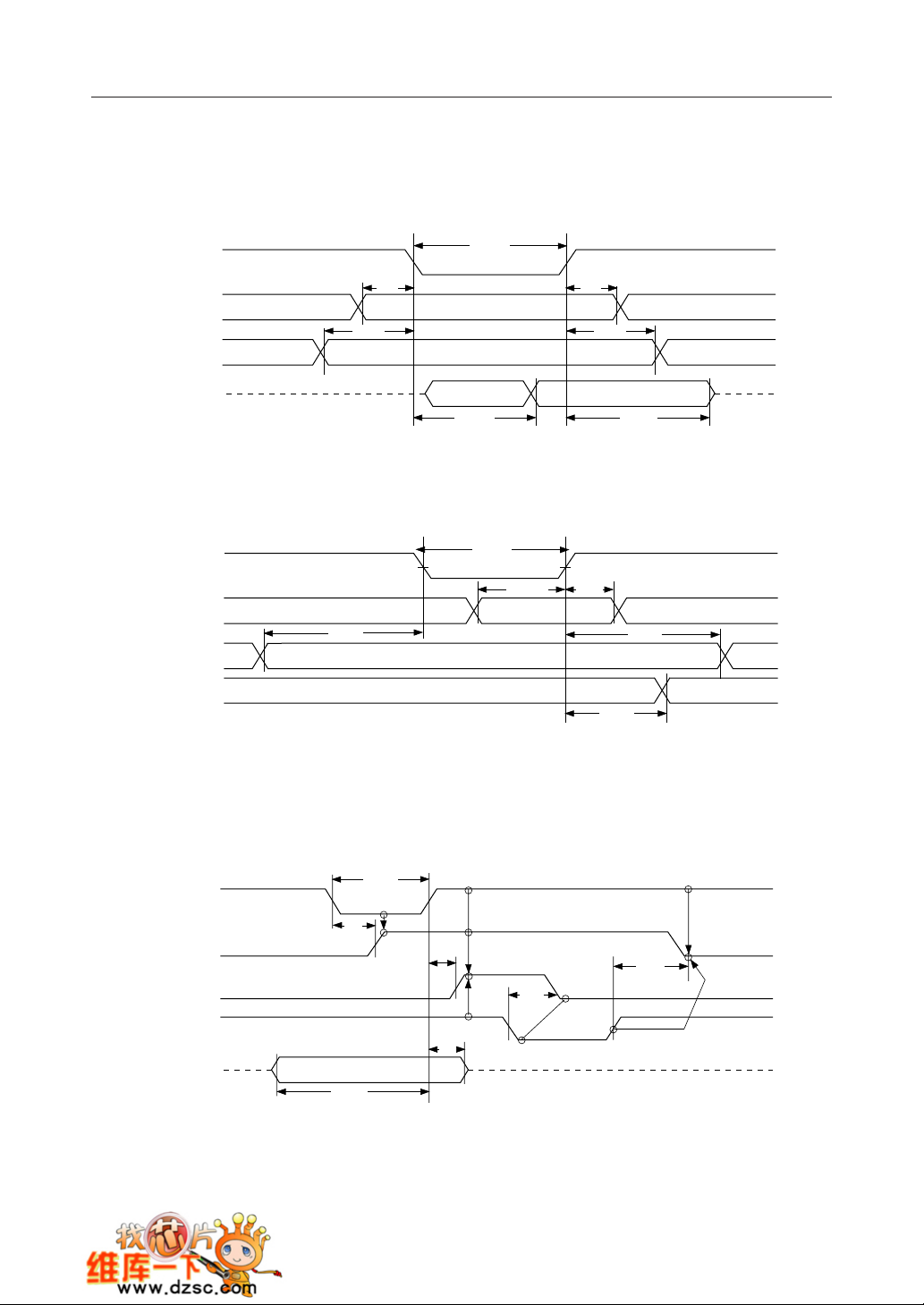
TIMING DIAGRAM
Basic Input Operation (Mode 0)
t
RR
RD
Port Input
t
, A
CS, A
1
0
D7 - D
0
Basic Output Operation (Mode 0)
WR
D7 - D
0
t
AW
, A
CS, A
1
0
AR
t
IR
t
RD
t
WW
t
DW
t
HR
t
RA
t
DF
t
WD
t
WA
Port Output
Strobe Input Operation (Mode 1)
STB
t
SIB
IBF
INTR
RD
Port Input
t
PS
t
WB
t
ST
t
SIT
t
RIT
t
PH
t
RIB
6/26
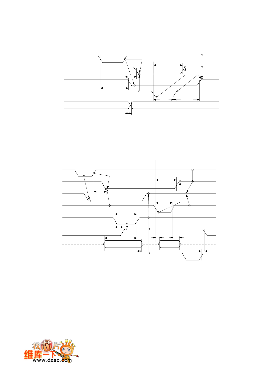
¡ Semiconductor MSM82C55A-2RS/GS/VJS
Strobe Output Operation (Mode 1)
WR
t
AOB
OBF
t
WOB
INTR
t
WIT
ACK
t
AK
t
AIT
Port Output
t
WB
Bidirectional Bus Operation (Mode 2)
WR
OBF
INTR
ACK
STB
IBF
Port A
RD
t
WOB
t
AOB
t
AK
t
ST
t
SIB
t
t
PS
t
AD
PH
t
KD
t
RIB
7/26
¡ Semiconductor MSM82C55A-2RS/GS/VJS
OUTPUT CHARACTERISTICS (REFERENCE VALUE)
1 Output "H" Voltage (VOH) vs. Output Current (IOH)
5
4
(V)
OH
3
2
1
Output "H" Voltage V
0
0 –1–2–3–4–5
Output Current IOH (mA)
Ta = –40 to + 85°C
VCC = 5.0 V
2 Output "L" Voltage (VOL) vs. Output Current (IOL)
5
4
(V)
OL
3
2
1
Output "L" Voltage V
0
012345
VCC = 5.0 V
Ta = –40 to +85°C
Output Current IOL (mA)
Note: The direction of flowing into the device is taken as positive for the output current.
8/26

¡ Semiconductor MSM82C55A-2RS/GS/VJS
PIN DESCRIPTION
Pin No.
D7 - D
RESET
CS
0
Item
Bidirectional
Data Bus
Reset Input
Chip Select
Input/Output
Input and
Input
RD
Read Input Input
WR Write Input Input
, A
0
1
Port Select Input
(Address)
A
Output
Input
Input
Input
Function
These are three-state 8-bit bidirectional buses used to write and
read data upon receipt of the WR and RD signals from CPU and also
used when control words and bit set/reset data are transferred from
CPU to MSM82C55A-2.
This signal is used to reset the control register and all internal
registers when it is in high level. At this time, ports are all made into
the input mode (high impedance status).
all port latches are cleared to 0.
and all ports groups are set to mode 0.
When the CS is in low level, data transmission is enabled with CPU.
When it is in high level, the data bus is made into the high impedance
status where no write nor read operation is performed. Internal
registers hold their previous status, however.
When RD is in low level, data is transferred from MSM82C55A-2 to
CPU.
When WR is in low level, data or control words are transferred from
CPU to MSM82C55A-2.
By combination of A
and A1, either one is selected from among
0
port A, port B, port C, and control register. These pins are usually
connected to low order 2 bits of the address bus.
PA7 - PA
PB7 - PB
- PC
PC
7
V
CC
0
0
0
Port A
Port B
Port C
––
GND – –
Input and
Output
Input and
Output
Input and
Output
These are universal 8-bit I/O ports. The direction of inputs/ outputs
can be determined by writing a control word. Especially, port A can
be used as a bidirectional port when it is set to mode 2.
These are universal 8-bit I/O ports. The direction of inputs/outputs
ports can be determined by writing a control word.
These are universal 8-bit I/O ports. The direction of inputs/outputs
can be determined by writing a control word as 2 ports with 4 bits
each. When port A or port B is used in mode 1 or mode 2 (port A
only), they become control pins. Especially, when port C is used as
an output port, each bit can set/reset independently.
+5V power supply.
GND
9/26

¡ Semiconductor MSM82C55A-2RS/GS/VJS
BASIC FUNCTIONAL DESCRIPTION
Group A and Group B
When setting a mode to a port having 24 bits, set it by dividing it into two groups of 12 bits each.
Group A: Port A (8 bits) and high order 4 bits of port C (PC7~PC4)
Group B: Port B (8 bits) and low order 4 bits of port C (PC3~PC0)
Mode 0, 1, 2
There are 3 types of modes to be set by grouping as follows:
Mode 0: Basic input operation/output operation (Available for both groups A and B)
Mode 1: Strobe input operation/output operation (Available for both groups A and B)
Mode 2: Bidirectional bus operation (Available for group A only)
When used in mode 1 or mode 2, however, port C has bits to be defined as ports for control signal
for operation ports (port A for group A and port B for group B) of their respective groups.
Port A, B, C
The internal structure of 3 ports is as follows:
Port A: One 8-bit data output latch/buffer and one 8-bit data input latch
Port B: One 8-bit data input/output latch/buffer and one 8-bit data input buffer
Port C: One 8-bit data output latch/buffer and one 8-bit data input buffer (no latch for input)
Single bit set/reset function for port C
When port C is defined as an output port, it is possible to set (to turn to high level) or reset (to
turn to low level) any one of 8 bits individually without affecting other bits.
10/26

¡ Semiconductor MSM82C55A-2RS/GS/VJS
OPERATIONAL DESCRIPTION
Control Logic
Operations by addresses and control signals, e.g., read and write, etc. are as shown in the table
below:
Operaiton OperationA
Input
A
1
0
0 0 Port A Æ Data Bus
0
0011
1001
00
0
Output
0010
1000
Control 1 0
Others
1
10
1
¥ 1¥ ¥
CS
WR
1
0
0
1
RD
0
0
0
1
1
1
1
0
¥
Port B Æ Data Bus
Port C Æ Data Bus
Data Bus Æ Port A
Data Bus Æ Port B
Data Bus Æ Port C
Data Bus Æ Control Register
Illegal Condition
Data bus is in the high impedance status.
Setting of Control Word
The control register is composed of 7-bit latch circuit and 1-bit flag as shown below.
Group A Control Bits Group B Control Bits
D
D
D
D
D
D
D
D
6
7
4
5
2
3
Control word Identification flag
Be sure to set 1 for the control word
to define a mode and input/output.
When set to 0, it becomes
the control word for bit set/
reset.
0
1
Definition of input/
output of low order
0 = Output
1 = Input
4 bits of port C.
Definition of input/
output of 8 bits of
0 = Output
1 = Input
port B.
Mode definition of
group B.
Definition of input/
output of high order
4 bits of port C.
Definition of input/
output of 8 bits of
0 = Mode 0
1 = Mode 1
0 = Output
1 = Input
0 = Output
1 = Input
port A.
Mode definition of group A.
D6D
Mode
5
0 0 Mode 0
0 1 Mode 1
1 ¥ Mode 2
11/26

¡ Semiconductor MSM82C55A-2RS/GS/VJS
Precaution for Mode Selection
The output registers for ports A and C are cleared to f each time data is written in the command
register and the mode is changed, but the port B state is undefined.
Bit Set/Reset Function
When port C is defined as output port, it is possible to set (set output to 1) or reset (set output
to 0) any one of 8 bits without affecting other bits as shown below.
D
D
D
D
D
D
D
D
6
7
4
5
2
3
0
1
Definition of set/reset
for a desired bit.
0 = Reset
1 = Set
Definition of bit wanted
to be set or reset.
Port C
Dont's Care
Control word Identification flag
Be sure to set to 0 for bit set/reset
When set to 1, it becomes the control
word to define a mode and input/output.
D3D
0 0PC
0
0 0PC
1
0 1PC
2
0 1PC
3
1 0PC
4
1 0PC
5
1 1PC
6
1 1PC
7
D
2
1
0
1
0
1
0
1
0
1
Interrupt Control Function
When the MSM82C55A-2 is used in mode 1 or mode 2, the interrupt signal for the CPU is
provided. The interrupt request signal is output from port C. When the internal flip-flop INTE
is set beforehand at this time, the desired interrupt request signal is output. When it is reset
beforehand, however, the interrupt request signal is not output. The set/reset of the internal
flip-flop is made by the bit set/reset operation for port C virtually.
Bit set Æ INTE is set Æ Interrupt allowed
Bit reset Æ INTE is reset Æ Interrupt inhibited
Operational Description by Mode
1. Mode 0 (Basic input/output operation)
Mode 0 makes the MSM82C55A-2 operate as a basic input port or output port. No control
signals such as interrupt request, etc. are required in this mode. All 24 bits can be used as
two-8-bit ports and two 4-bit ports. Sixteen combinations are then possible for inputs/
outputs. The inputs are not latched, but the outputs are.
12/26

¡ Semiconductor MSM82C55A-2RS/GS/VJS
Control Word Group A Group B
Type
1
2
3
4
5
6
7
8
9
10
11
12
13
14
15
16
D
D
D
D
D
D
7
6
5
4
1
0
0
0
1
0
0
0
1
0
0
0
1
0
0
0
1
0
0
0
1
0
0
0
1
0
0
0
1
0
0
0
1
0
0
1
1
0
0
1
1
0
0
1
1
0
0
1
1
0
0
1
1
0
0
1
1
0
0
1
1
0
0
1
D
3
2
1
0
0
0
0
0
0
0
0
1
0
0
1
1
0
0
1
0
0
1
0
1
1
0
1
0
0
0
0
0
0
0
0
1
0
0
1
1
0
0
1
0
0
1
0
1
1
0
1
Port A
D
0
Output
0
Output
1
0
Output
1
Output
0
Output
1
Output
0
Output
1
Output
0
Input
1
Input
0
Input
1
Input
0
Input
1
Input
0
Input
1
Input
High Order 4 Bits
of Port C
Output
Output
Output
Output
Input
Input
Input
Input
Output
Output
Output
Output
Input
Input
Input
Input
Port B
Output
Output
Input
Input
Output
Output
Input
Input
Output
Output
Input
Input
Output
Output
Input
Input
Low Order 4 Bits
of Port C
Output
Input
Output
Input
Output
Input
Ouput
Input
Output
Input
Output
Input
Output
Input
Output
Input
Notes: When used in mode 0 for both groups A and B
2. Mode 1 (Strobe input/output operation)
In mode 1, the strobe, interrupt and other control signals are used when input/output
operations are made from a specified port. This mode is available for both groups A and
B. In group A at this time, port A is used as the data line and port C as the control signal.
Following is a description of the input operation in mode 1.
STB (Strobe input)
When this signal is low level, the data output from terminal to port is fetched into the
internal latch of the port. This can be made independent from the CPU, and the data is not
output to the data bus until the RD signal arrives from the CPU.
IBF (Input buffer full flag output)
This is the response signal for the STB. This signal when turned to high level indicates that
data is fetched into the input latch. This signal turns to high level at the falling edge of STB
and to low level at the rising edge of RD.
INTR (Interrupt request output)
This is the interrupt request signal for the CPU of the data fetched into the input latch. It
is indicated by high level only when the internal INTE flip-flop is set. This signal turns to
high level at the rising edge of the STB (IBF = 1 at this time) and low level at the falling edge
of the RD when the INTE is set.
INTE A of group A is set when the bit for PC4 is set, while INTE B of group B is set when the
bit for PC2 is set.
Following is a description of the output operation of mode 1.
13/26

¡ Semiconductor MSM82C55A-2RS/GS/VJS
OBF (Output buffer full flag output)
This signal when turned to low level indicates that data is written to the specified port upon
receipt of the WR signal from the CPU. This signal turns to low level at the rising edge of
the WR and high level at the falling edge of the ACK.
ACK (Acknowledge input)
This signal when turned to low level indicates that the terminal has received data.
INTR (Interrupt request output)
This is the signal used to interrupt the CPU when a terminal receives data from the CPU via
the MSM82C55A-5. It indicates the occurrence of the interrupt in high level only when the
internal INTE flip-flop is set. This signal turns to high level at the rising edge of the ACK
(OBF = 1 at this time) and low level at the falling edge of WR when the INTE B is set.
INTE A of group A is set when the bit for PC6 is set, while INTE B of group B is set when the
bit for PC2 is set.
Mode 1 Input
RD
Note: Although belonging to group B, PC3 operates as the control signal of
Mode 1 Output
(Group A)
PA
7
-
INTE
A
PA
0
PC
4
PC
5
PC
3
group A functionally.
(Group A)
PA
7
INTE
A
PA
PC
-
0
7
8
8
STB
IBF
INTR
OBF
(Group B)
PB
INTE
B
PB
A
A
PC
PC
8
7
-
0
STB
2
1
IBF
B
B
RD
A
PC
(Group B)
PB
INTE
B
PB
A
PC
INTR
0
B
8
7
-
0
OBF
1
B
WR
PC
PC
ACK
6
A
PC
ACK
2
B
WR
INTR
3
A
PC
INTR
0
B
14/26

¡ Semiconductor MSM82C55A-2RS/GS/VJS
Port C Function Allocation in Mode 1
Combination of
Input/Output
Port C
PC
PC
PC
PC
PC
PC
PC
PC
0
1
2
3
4
5
6
7
Group A: Input
Group B: Input
INTR
B
IBF
B
STB
B
INTR
A
STB
A
IBF
A
I/O I/O
I/O I/O
Group A: Input
Group B: Output
INTR
B
OBF
B
ACK
B
INTR
A
STB
A
IBF
A
Group A: Output
Group B: Input
INTR
B
IBF
B
STB
B
INTR
A
I/O
I/O
ACK
A
OBF
A
Group A: Output
Group B: Output
INTR
OBF
ACK
INTR
I/O
I/O
ACK
OBF
Note: I/O is a bit not used as the control signal, but it is available as a port of mode 0.
Examples of the relation between the control words and pins when used in mode 1 are
shown below:
(a) When group A is mode 1 output and group B is mode 1 input.
D7D6D5D4D3D2D1D
Control Word
0
¥111/00101
B
B
B
A
A
A
WR
RD
PA7 - PA
PC
PC
PC
PC4, PC
PB7 - PB
PC
PC
PC
Selection of I/O
of PC
and PC
4
when not defined
as a control pin.
1 = Input
0 = Output
8
0
OBF
7
ACK
6
INTR
3
2
I/O
5
8
0
STB
2
IBF
1
0
B
INTR
As all of PC0 - PC3 bits
become a control pin
5
in this case, this bit is
"Don't Care".
A
A
A
Group A: Mode 1 Output
Group B: Mode 1 Input
B
B
15/26

¡ Semiconductor MSM82C55A-2RS/GS/VJS
(b) When group A is mode 1 input and group B is mode 1 output.
D7D6D5D4D3D2D1D
0
¥011/01101
Selection of I/O of PC6 and PC
7
when not defined as a control pin.
1 = Input
0 = Output
PC
PC
PC
PC
PC
PC
8
0
STB
4
5
3
7
0
1
2
0
A
IBF
A
INTR
I/O
OBF
ACK
INTR
A
Group A: Mode 1 Input
Group B: Mode 1 Output
B
B
B
2
2
8
8
PA7 - PA
RD
PC6, PC
PB7 - PB
WR
3. Mode 2 (Strobe bidirectional bus I/O operation)
In mode 2, it is possible to transfer data in 2 directions through a single 8-bit port. This
operation is akin to a combination between input and output operations. Port C waits for
the control signal in this case, too. Mode 2 is available only for group A, however.
Next, a description is made on mode 2.
OBF (Output buffer full flag output)
This signal when turned to low level indicates that data has been written to the internal
output latch upon receipt of the WR signal from the CPU. At this time, port A is still in the
high impedance status and the data is not yet output to the outside. This signal turns to low
level at the rising edge of the WR and high level at the falling edge of the ACK.
ACK (Acknowledge input)
When a low level signal is input to this pin, the high impedance status of port A is cleared,
the buffer is enabled, and the data written to the internal output latch is output to port A.
When the input returns to high level, port A is made into the high impedance status.
STB (Strobe input)
When this signal turns to low level, the data output to the port from the pin is fetched into
the internal input latch. The data is output to the data bus upon receipt of the RD signal from
the CPU, but it remains in the high impedance status until then.
IBF (Input buffer full flag output)
This signal when turned to high level indicates that data from the pin has been fetched into
the input latch. This signal turns to high level at the falling edge of the STB and low level
at the rising edge of the RD.
16/26

¡ Semiconductor MSM82C55A-2RS/GS/VJS
INTR (Interrupt request output)
This signal is used to interrupt the CPU and its operation in the same as in mode 1. There
are two INTE flip-flops internally available for input and output to select either interrupt
of input or output operation. The INTE1 is used to control the interrupt request for output
operation and it can be reset by the bit set for PC6. INTE2 is used to control the interrupt
request for the input operation and it can be set by the bit set for PC4.
Mode 2 I/O Operation
INTE
1
WR
RD
INTE
2
Port C Function Allocation in Mode 2
Port C
PC
0
PC
PC
PC
PC
PC
PC
PC
1
2
3
4
5
6
7
Confirmed to the Group B Mode
PC
3
PA
7
-
PA
0
PC
7
PC
6
PC
4
PC
5
Function
INTR
A
STBA
IBF
A
ACK
A
OBF
A
INTR
A
8
OBF
A
ACK
A
STB
A
IBF
A
Following is an example of the relation between the control word and the pin when used in
mode 2.
When input in mode 2 for group A and in mode 1 for group B.
17/26

¡ Semiconductor MSM82C55A-2RS/GS/VJS
D7D6D5D4D3D2D1D
As all of 8 bits of port C become
control pins in this case, D
D
bits are treated as "Don't Care".
0
No I/O specification is required for mode 2,
since it is a bidirectional operation.
This bit is therefore treated as "Don't Care".
When group A is set to mode 2, this bit is treated
as "Don't Care".
PC
3
PC
PC
PC
PC
PC
PC
PC
8
0
7
6
4
5
8
0
2
1
0
RD
WR
PA7 - PA
PB7 - PB
0
¥11¥¥¥11
INTR
OBF
ACK
STB
IBF
STB
IBF
INTR
and
3
A
A
A
A
A
B
B
Group A: Mode 2
Group B: Mode 1 Input
B
18/26

¡ Semiconductor MSM82C55A-2RS/GS/VJS
4. When Group A is Different in Mode from Group B
Group A and group B can be used by setting them in different modes each other at the same
time. When either group is set to mode 1 or mode 2, it is possible to set the one not defined
as a control pin in port C to both input and output as port which operates in mode 0 at the
3rd and 0th bits of the control word.
(Mode combinations that define no control bit at port C)
Group A Group B
Mode 1
1
input
Mode 0
2
Output
Mode 0
3
4
Mode 0
Mode 1
5
Input
Mode 1
6
Input
Mode 1
7
Output
Mode 1
8
Output
Mode 2
9
Mode 0
Mode 0
Mode 1
Input
Mode 1
Output
Mode 1
Input
Mode 1
Output
Mode 1
Input
Mode 1
Output
Mode 0
PC
PC
7
I/O I/O IBF
OBF
ACK
A
PC
6
A
5
A
I/O
I/O I/O I/O
I/O I/O I/O
I/O I/O IBF
I/O I/O IBF
OBF
OBF
OBF
ACK
A
A
A
ACK
ACK
A
A
A
I/O
I/O
IBF
A
A
A
Controlled at the 3rd bit (D3) of
the Control Word
Port C
PC
STB
I/O INTR
PC
4
A
INTR
3
A
A
I/O I/O STB
I/O I/O ACK
STB
STB
I/O INTR
I/O INTR
STB
INTR
A
A
A
INTR
INTR
A
A
STB
A
ACK
A
A
Controlled at the 0th bit (D0) of
the Control Word
PC
I/O
I/O
STB
ACK
I/O
2
B
B
B
B
B
B
PC
1
I/O
I/O I/O
IBF
B
OBF
B
IBF
B
OBF
B
IBF
B
OBF
B
I/O I/O
INTR
INTR
INTR
INTR
INTR
INTR
When the I/O bit is set to input in this case, it is possible to access data by the normal port
C read operation.
When set to output, PC7-PC4 bits can be accessed by the bit set/reset function only.
Meanwhile, 3 bits from PC2 to PC0 can be accessed by normal write operation.
The bit set/reset function can be used for all of PC3-PC0 bits. Note that the status of port C
varies according to the combination of modes like this.
PC
I/O
0
B
B
B
B
B
B
19/26

¡ Semiconductor MSM82C55A-2RS/GS/VJS
5. Port C Status Read
When port C is used for the control signal, that is, in either mode 1 or mode 2, each control
signal and bus status signal can be read out by reading the content of port C.
The status read out is as follows:
Group A Group B
Mode 1
1
Input
Mode 1
2
Output
Mode 0
3
4
Mode 0
Mode 1
5
Input
Mode 1
6
Input
Mode 1
7
Output
Mode 1
8
Output
Mode 2
9
Mode 2
10
Mode 0
Mode 0
Mode 1
Input
Mode 1
Output
Mode 1
Input
Mode 1
Output
Mode 1
Input
Mode 1
Output
Mode 0
Mode 1
Input
D
D
7
6
I/O I/O IBF
OBF
INTE
A
A
I/O I/O I/O
I/O I/O I/O
I/O I/O IBF
I/O I/O IBF
OBF
OBF
OBF
OBF
INTE
A
A
A
A
INTE
INTE
INTE
A
A
1
1
Status Read on the Data Bus
D
I/O
5
A
D
4
INTE
A
I/O INTR
D
INTR
3
A
A
I/O I/O INTE
I/O I/O INTE
I/O
I/O
IBF
IBF
A
A
A
A
INTE
INTE
I/O INTR
I/O INTR
INTE
INTE
INTR
A
A
2
2
INTR
INTR
INTR
A
A
A
A
A
A
D
I/O
I/O
INTE
INTE
INTE
INTE
I/O
INTE
2
B
B
B
B
B
B
B
D
1
I/O
I/O I/O
IBF
B
OBF
B
IBF
B
OBF
B
IBF
OBF
INTR
B
INTR
B
I/O I/O
IBF
B
D
I/O
INTR
INTR
INTR
INTR
INTR
0
B
B
B
B
B
B
B
11
Mode 2
Mode 1
Output
OBF
INTE
A
IBF
1
INTE
A
INTR
2
INTE
A
OBF
B
B
6. Reset of MSM82C55A-2
Be sure to keep the RESET signal at power ON in the high level at least for 50 ms.
Subsequently, it becomes the input mode at a high level pulse above 500 ns.
Note: Comparison of MSM82C55A-5 and MSM82C55A-2
MSM82C55A-5
After a write command is executed to the command register, the internal latch is cleared in
PORTA PORTC. For instance, 00H is output at the beginning of a write command when
the output port is assigned. However, if PORTB is not cleared at this time, PORTB is
unstable. In other words, PORTB only outputs ineffective data (unstable value according
to the device) during the period from after a write command is executed till the first data
is written to PORTB.
MSM82C55A-2
After a write command is executed to the command register, the internal latch is cleared in
All Ports (PORTA, PORTB, PORTC). 00H is output at the beginning of a write command
when the output port is assigned.
INTR
20/26
B

¡ Semiconductor MSM82C55A-2RS/GS/VJS
NOTICE ON REPLACING LOW-SPEED DEVICES WITH HIGH-SPEED DEVICES
The conventional low speed devices are replaced by high-speed devices as shown below.
When you want to replace your low speed devices with high-speed devices, read the replacement
notice given on the next pages.
High-speed device (New)
M80C85AH
M80C86A-10
M80C88A-10
M82C84A-2
M81C55-5
M82C37B-5
M82C51A-2
M82C53-2
M82C55A-2
Low-speed device (Old)
M80C85A/M80C85A-2
M80C86A/M80C86A-2
M80C88A/M80C88A-2
M82C84A/M82C84A-5
M81C55
M82C37A/M82C37A-5
M82C51A
M82C53-5
M82C55A-5
Remarks
8bit MPU
16bit MPU
8bit MPU
Clock generator
RAM.I/O, timer
DMA controller
USART
Timer
PPI
21/26

¡ Semiconductor MSM82C55A-2RS/GS/VJS
Differences between MSM82C55A-5 and MSM82C55A-2
1) Manufacturing Process
These devices use a 3 m Si-Gate CMOS process technology.
The MSM82C55A-2 is about 7% smaller in chip size than the MSM82C55A-5 as the MSM82C55A2 changed its output characteristics.
2) Function
Item
Internal latch during writing into
the command register
Only ports A and C are cleared.
Port B is not cleared.
MSM82C55A-5
MSM82C55A-2
All ports are cleared.
The above function has been improved to remove bugs and other logics are not different between
the two devices.
3) Electrical Characteristics
3-1) DC Characteristics
Parameter
''L'' Output Voltage
''H'' Output Voltage
Average Operating Current
Symbol
V
OL
V
OH
I
CC
MSM82C55A-5 MSM82C55A-2
0.45 V
= +2.5 mA)
(I
OL
2.4 V
(I
= -400 mA)
OH
5 mA maximum
(I/O Cycle = 1 ms)
0.40 V
(I
= +2.5 mA)
OL
3.7 V
(I
= -2.5 mA)
OH
8 mA maximum
(I/O Cycle = 375 ns)
As shown above, the DC characteristics of the MSM82C55A-2 satisfies the DC characteristics of the
MSM82C55A-5.
3-2) AC Characteristics
Parameter
Address Hold Time for RD Rising 20 ns minimum 0 ns minimum
RD Pulse Width 300 ns minimum 100 ns minimum
Difined Data Output Delay Time
From RD Falling
Data Floating Delay Time From RD Rising
RD/WR Recovery Time
Symbol
t
RA
t
RR
t
RD
t
RF
t
RV
MSM82C55A-5 MSM82C55A-2
200 ns maximum 120 ns maximum
100 ns maximum 75 ns maximum
850 ns minimum 200 ns minimum
22/26

¡ Semiconductor MSM82C55A-2RS/GS/VJS
Parameter
Address Hold Time for WR Rising
WR Pulse Width 300 ns minimum 150 ns minimum
Data Setup Time for WR Rising
Data Hold Time for WR Rising
Defined Data Output Time
From WR Rising
Port Data Hold Time for RD Rising 20 ns minimum 10 ns minimum
ACK Pulse Width 300 ns minimum 100 ns minimum
STB Pulse Width 300 ns minimum 100 ns minimum
Port Data Hold Time for STB Falling 180 ns minimum 50 ns minimum
ACK Falling to Defined Data Output 300 ns maximum 150 ns maximum
WR Falling to OBF Falling Delay Time 650 ns maximum 150 ns maximum
Symbol
t
WA
t
WW
t
DW
t
WD
WB
t
HR
t
AK
t
ST
t
PH
t
AD
t
WOB
MSM82C55A-5 MSM82C55A-2
30 ns minimum 20 ns minimum
1000 ns minimum 50 ns minimum
40 ns minimum 30 ns minimum
350 ns maximum 200 ns maximumt
t
ACK Falling to OBF Rising Delay Time 350 ns maximum 150 ns maximum
STB Falling to IBF Rising Delay Time 300 ns maximum 150 ns maximum
RD Rising to IBF Falling Delay Time 300 ns maximum 150 ns maximum
RD Falling to INTR Falling Delay Time 400 ns maximum 200 ns maximum
STB Rising to INTR Rising Delay Time 300 ns maximum 150 ns maximum
ACK Rising to INTR Rising Delay Time 350 ns maximum 150 ns maximum
WR Falling to INTR Falling Delay Time 850 ns minimum 250 ns maximum
AOB
t
t
t
t
t
t
WIT
SIB
RIB
RIT
SIT
AIT
As shown above, the MSM82C55A-2 satisfies the characteristics of the MSM82C55A-5.
23/26

¡ Semiconductor MSM82C55A-2RS/GS/VJS
PACKAGE DIMENSIONS
(Unit : mm)
DIP40-P-600-2.54
Package material
Lead frame material
Pin treatment
Solder plate thickness
Package weight (g)
Epoxy resin
42 alloy
Solder plating
5 mm or more
6.10 TYP.
Notes for Mounting the Surface Mount Type Package
The SOP, QFP, TSOP, SOJ, QFJ (PLCC), SHP and BGA are surface mount type packages, which
are very susceptible to heat in reflow mounting and humidity absorbed in storage.
Therefore, before you perform reflow mounting, contact Oki’s responsible sales person for the
product name, package name, pin number, package code and desired mounting conditions
(reflow method, temperature and times).
24/26

¡ Semiconductor MSM82C55A-2RS/GS/VJS
(Unit : mm)
QFJ44-P-S650-1.27
Mirror finish
Package material
Lead frame material
Pin treatment
Solder plate thickness
Package weight (g)
Epoxy resin
Cu alloy
Solder plating
5 mm or more
2.00 TYP.
Notes for Mounting the Surface Mount Type Package
The SOP, QFP, TSOP, SOJ, QFJ (PLCC), SHP and BGA are surface mount type packages, which
are very susceptible to heat in reflow mounting and humidity absorbed in storage.
Therefore, before you perform reflow mounting, contact Oki’s responsible sales person for the
product name, package name, pin number, package code and desired mounting conditions
(reflow method, temperature and times).
25/26

¡ Semiconductor MSM82C55A-2RS/GS/VJS
(Unit : mm)
QFP44-P-910-0.80-2K
Mirror finish
Package material
Lead frame material
Pin treatment
Solder plate thickness
Package weight (g)
Epoxy resin
42 alloy
Solder plating
5 mm or more
0.41 TYP.
Notes for Mounting the Surface Mount Type Package
The SOP, QFP, TSOP, SOJ, QFJ (PLCC), SHP and BGA are surface mount type packages, which
are very susceptible to heat in reflow mounting and humidity absorbed in storage.
Therefore, before you perform reflow mounting, contact Oki’s responsible sales person for the
product name, package name, pin number, package code and desired mounting conditions
(reflow method, temperature and times).
26/26
 Loading...