


E2O0018-27-X2
¡ Semiconductor MSM82C53-2RS/GS/JS
¡ Semiconductor
This version: Jan. 1998
Previous version: Aug. 1996
MSM82C53-2RS/GS/JS
CMOS PROGRAMMABLE INTERVAL TIMER
GENERAL DESCRIPTION
The MSM82C53-2RS/GS/JS is programmable universal timers designed for use in
microcomputer systems. Based on silicon gate CMOS technology, it requires a standby current
of only 100 mA (max.) when the chip is in the nonselected state. During timer operation, power
consumption is still very low only 8 mA (max.) at 8 MHz of current required.
The device consists of three independent counters, and can count up to a maximum of 8 MHz
(MSM82C53-2). The timer features six different counter modes, and binary count/BCD count
functions. Count values can be set in byte or word units, and all functions are freely
programmable.
FEATURES
• Maximum operating frequency of 8 MHz (MSM82C53-2)
• High speed and low power consumption achieved through silicon gate CMOS technology
• Completely static operation
• Three independent 16-bit down-counters
• 3 V to 6 V single power supply
• Six counter modes available for each counter
• Binary and decimal counting possible
• 24-pin Plastic DIP (DIP24-P-600-2.54): (Product name: MSM82C53-2RS)
• 28-pin Plastic QFJ (QFJ28-P-S450-1.27): (Product name: MSM82C53-2JS)
• 32-pin Plastic SSOP(SSOP32-P-430-1.00-K): (Product name: MSM82C53-2GS-K)
1/19
¡ Semiconductor MSM82C53-2RS/GS/JS
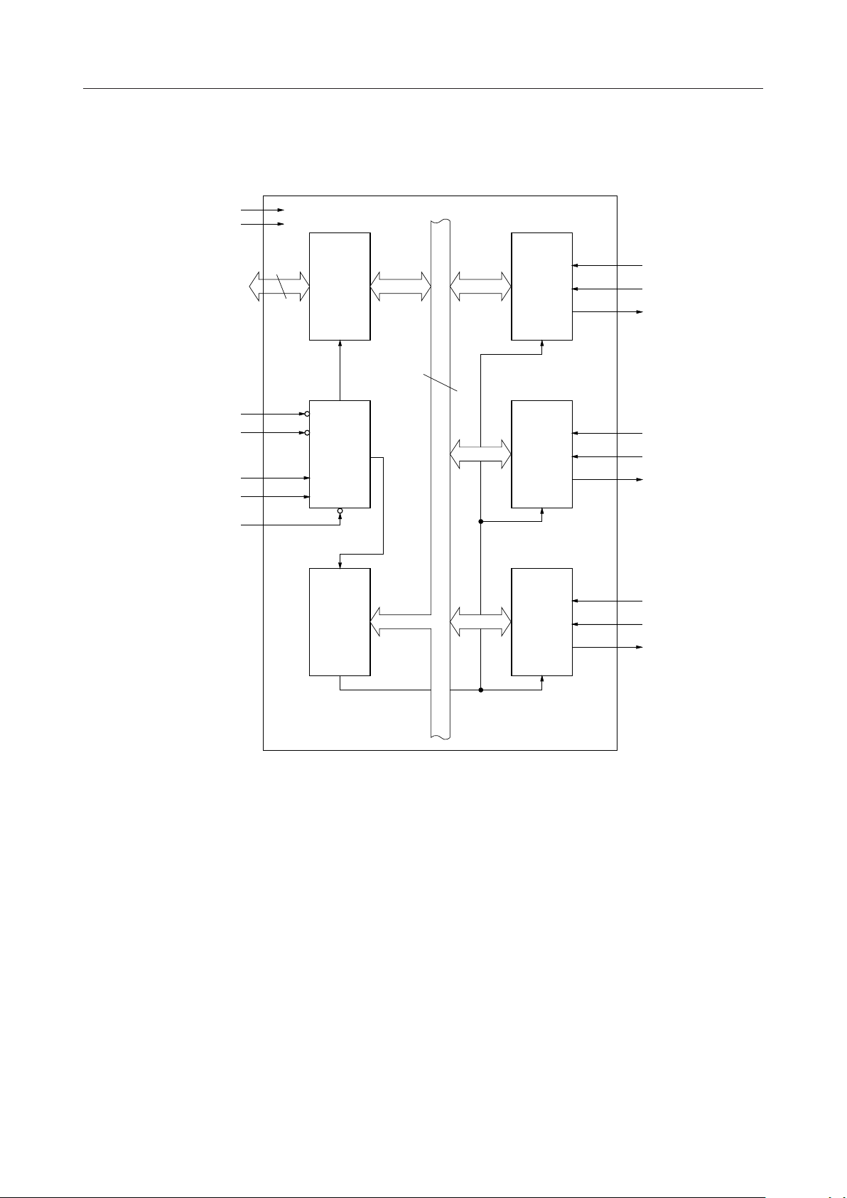
FUNCTIONAL BLOCK DIAGRAM
V
CC
GND
8
D
- D
7
0
Data
Bus
Buffer
Counter
#0
CLK
GATE
OUT
0
0
0
8
WR
RD
A
A
Read/
Write
0
1
Logic
Counter
#1
CLK
GATE
OUT
1
1
1
CS
Control
Word
Register
Counter
#2
CLK
GATE
OUT
2
2
2
Internal Bus
2/19
¡ Semiconductor MSM82C53-2RS/GS/JS
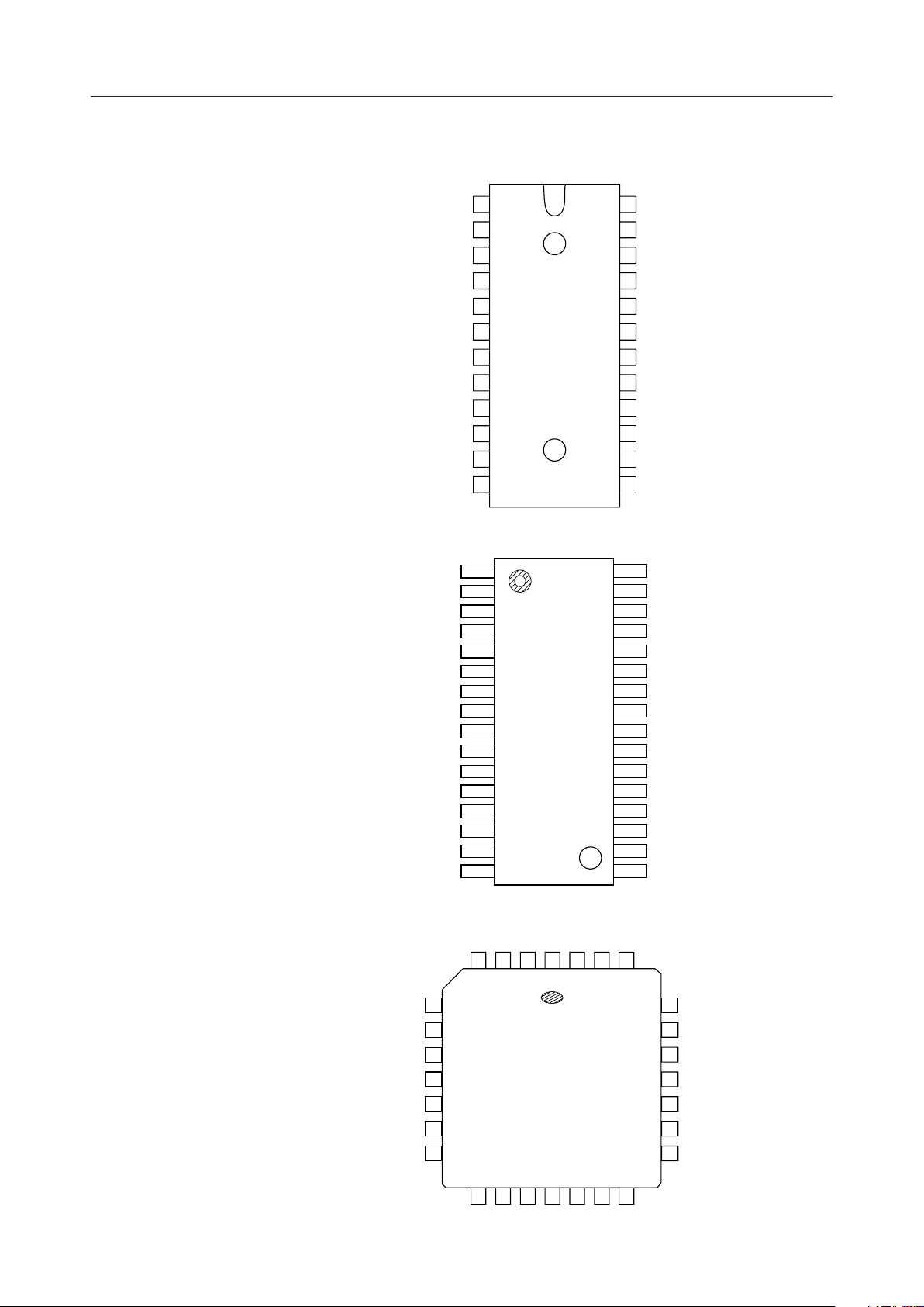
PIN CONFIGURATION (TOP VIEW)
24 pin Plastic DIP
32 pin Plastic SSOP
GATE
CLK
OUT
GATE
GND
CLK
OUT
GND
NC
D
7
D
6
D
5
NC
D
4
D
3
D
2
D
1
D
0
0
NC
0
0
NC
D
1
7
D
2
6
D
3
5
D
4
4
D
5
3
D
6
2
D
7
1
D
8
0
9
0
10
0
11
0
12
1
2
3
4
5
6
7
8
9
10
11
12
13
14
15
16
24
23
22
21
20
19
18
17
16
15
14
13
32
31
30
29
28
27
26
25
24
23
22
21
20
19
18
17
V
cc
WR
RD
CS
A
1
A
0
CLK
OUT
GATE
CLK
GATE
OUT
NC
V
cc
WR
RD
NC
CS
A
1
A
0
CLK
OUT
GATE
NC
CLK
GATE
OUT
NC
2
2
2
1
1
1
2
2
2
1
1
1
(NC denotes "not connected")
28 pin Plastic QFJ
CLK
D
D
D
D
D
NC
5D6D7
D
4
3
2
5
4
6
3
7
2
8
1
9
0
10
0
11
12
13
14
GATE0
GND
OUT0
NC
1
15
NC
CC
V
28
16
1
OUT
WR
27
17
1
GATE
RD
26
18
1
CLK
25
24
23
22
21
20
19
NC
CS
A
1
A
0
CLK
OUT
GATE
2
2
2
3/19
¡ Semiconductor MSM82C53-2RS/GS/JS
ABSOLUTE MAXIMUM RATINGS
Parameter Units
Supply Voltage
Input Voltage
Output Voltage
Storage Temperature
Power Dissipation
Symbol
V
CC
V
IN
V
OUT
T
STG
P
D
Condition
Respect
to GND
—
Ta = 25°C
MSM82C53-2RS
MSM82C53-2GS MSM82C53-2JS
–0.5 to + 7
–0.5 to V
–0.5 to V
CC
CC
+ 0.5
+ 0.5
–55 to + 150
0.7
0.90.9
OPERATING RANGES
Rating
Parameter UnitSymbol
Supply Voltage
Operating Temperature
Condition
V
CC
T
op
VIL = 0.2 V, VIH = VCC -0.2 V,
Operating Frequency 2.6 MHz
Range
3 to 6
–40 to +85
RECOMMENDED OPERATING CONDITIONS
V
V
V
°C
W
V
°C
Parameter UnitSymbol
Supply Voltage
Operating Temperature
"L" Input Voltage V
"H" Input Voltage
Min.
V
CC
T
op
IL
V
IH
4.5
–40
–0.3
2.2
Typ.
5V
+25
—
—
Max.
+0.8
V
CC
5.5
+85
+ 0.3
DC CHARACTERISTICS
Parameter Unit
"L" Output Voltage
"H" Output Voltage
Input Leak Current
Output Leak Current
Standby Supply
Current
Operating Supply
Current
Symbol
V
OL
V
OH
I
LI
I
LO
I
CCS
I
CC
I
= 4 mA
OL
I
= –1 mA
OH
0 £ V
0 £ V
CS ≥ V
≥ V
V
IH
V
£ 0.2 V
IL
t
= 125 ns
CLK
C
= 0 pF
L
IN
OUT
CC
CC
£ V
£ V
- 0.2 V
- 0.2 V
Condition
CC
CC
= 4.5 V to 5.5 V
V
CC
Ta
= –40°C to +85°C
Min.
—
3.7
–10
–10
—
—
Typ. Max.
— 0.45 V
—— V
—10mA
—10mA
— 100 mA
—8mA
°C
V
V
4/19
¡ Semiconductor MSM82C53-2RS/GS/JS
AC CHARACTERISTICS
(V
= 4.5 V to 5.5 V, Ta = –40 to +85°C)
CC
Parameter
Address Set-up Time before Reading
Address Hold Time after Reading
Read Pulse Width
Read Recovery Time
Address Set-up Time before Writing
Address Hold Time after Writing
Write Pulse Width
Data Input Set-up Time before Writing
Data Input Hold Time after Writing
Write Recovery Time
Clock Cycle Time
Clock "H" Pulse Width
Clock "L" Pusle Width
"H" Gate Pulse Width
"L" Gate PUlse Width
Gate Input Set-up Time before Clock
Gate Input Hold Time after Clock
Output Delay Time after Reading
Output Floating Delay Time after
Reading
Output Delay Time after Gate
Output Delay Time after Clock
Output Delay Time after Address
Symbol Unit Condition
t
AR
t
RA
t
RR
t
RVR
t
AW
t
WA
t
WW
t
DW
t
WD
t
RVW
t
CLK
t
PWH
t
PWL
t
GW
t
GL
t
GS
t
GH
t
RD
t
DF
t
ODG
t
OD
t
AD
MSM82C53-2
Min.
30
0
150
200
0
20
150
100
20
200
125
60
60
50
50
50
50
—
5
—
—
—
Max.
—
—
—
—
—
—
—
—
—
—
D.C.
—
—
—
—
—
—
120
90
120
150
180
ns
ns Read
ns
Cycle
ns
ns
ns
ns Write
ns
Cycle
ns
ns
ns
ns
ns
ns
ns
ns
Clock
and
Gate
Timing
ns
ns
ns
ns
ns
Delay
Time
ns
= 150 pF
C
L
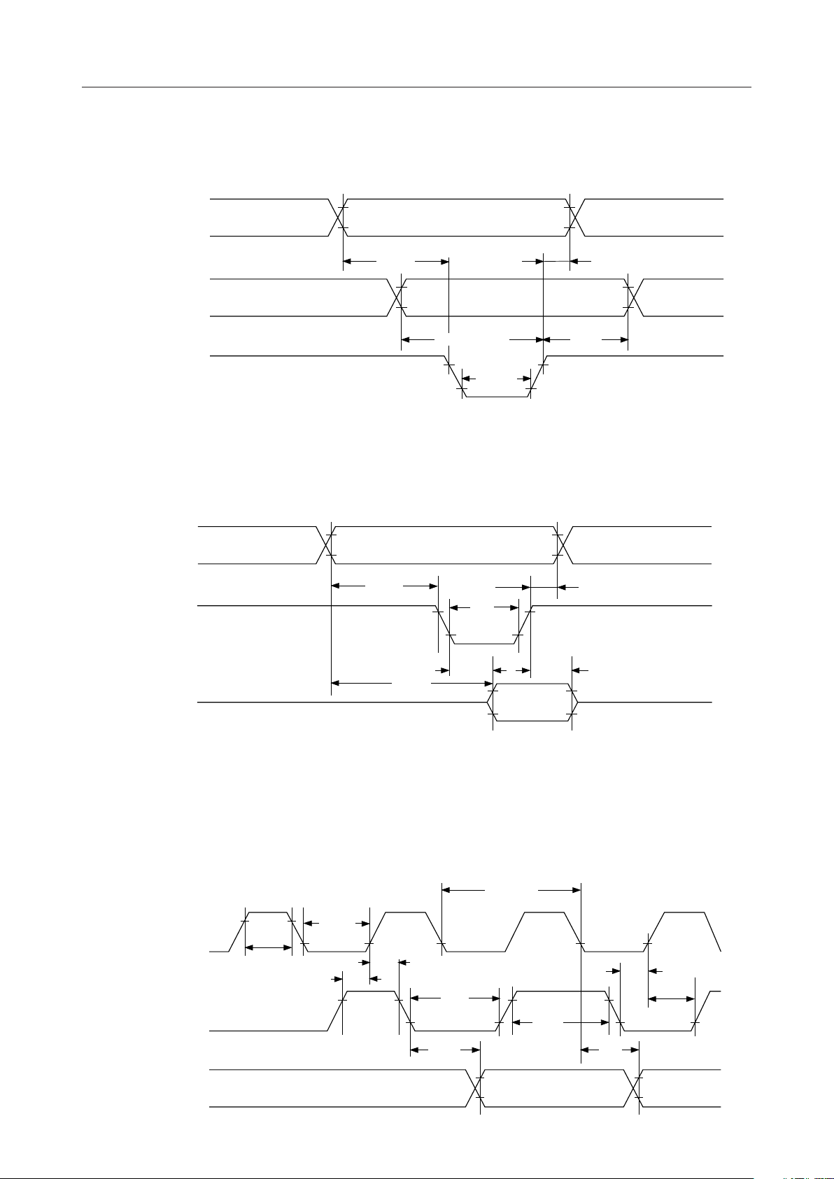
Note: Timing measured at VL = 0.8 V and VH = 2.2 V for both inputs and outputs.
5/19
¡ Semiconductor MSM82C53-2RS/GS/JS
TIMING CHART
WriteTiming
A
CS
0 - 1
Read Timing
A
0 - 7,
RD
D
CS
0 - 7
WR
t
AW
t
DW
t
WW
t
AR
t
RR
t
WD
t
RA
t
WA
D
0 - 7
Clock & Gate Timing
CLK
GATE
t
PWH
CLK
Valid
t
t
GW
DF
High ImpedanceHigh Impedance
t
GS
t
GH
t
OD
t
t
AD
RD
t
t
PWL
t
GH
t
GS
t
GL
t
ODG
OUT
6/19

¡ Semiconductor MSM82C53-2RS/GS/JS
DESCRIPTION OF PIN FUNCTIONS
Pin Symbol FunctionName
D7 - D
0
Bidirectional
Data Bus
Input/Output
Input/Output
Three-state 8-bit bidirectional data bus used when writing control words
and count values, and reading count values upon reception of WR and
RD signals from CPU.
Data transfer with the CPU is enabled when this pin is at low level. When
CS
Chip Select
Input
Input
at high level, the data bus (D
state where neither writing nor reading can be executed. Internal registers,
thru D7) is switched to high impedance
0
however, remain unchanged.
RD Data can be transferred from MSM82C53-2 to CPU when this pin is at low
Read Input Input
level.
WR Data can be transferred from CPU to MSM82C53-2 when this pin is at low
Write Input Input
level.
A0 - A
1
Address Input Input
One of the three internal counters or the control word register is selected
by A
combination. These two pins are normally connected to the two
0/A1
lower order bits of the address bus.
CLK0 -
2
Clock Input Input
Supply of three clock signals to the three counters incorporated in
MSM82C53-2.
GATE0 -
2
Gate Input Input
Control of starting, interruption, and restarting of counting in the three
respective counters in accordance with the set control word contents.
OUT0 -
Counter Output Output
2
Output of counter output waveform in accordance with the set mode and
count value.
SYSTEM INTERFACING
A1A
0
A1A0CS
Counter #0
OUT GATE CLK
Address Bus
Control Bus
Data Bus
8 bits
D
-
7
0
MSM82C53-2
Counter #1
OUT GATE CLK
16 bits
8 bits
RD WR
Counter #2
OUT GATE CLK
7/19

¡ Semiconductor MSM82C53-2RS/GS/JS
DESCRIPTION OF BASIC OPERATIONS
Data transfers between the internal registers and the external data bus is outlined in the
following table.
CS
0
0
0
0
0
0
0
0
1
0
RD
1
1
1
1
0
0
0
0
¥
1
WR
0
0
0
0
1
1
1
1
¥
1
A
A
1
0
0
1
1
0
0
1
1
¥
¥
0
0
1
0
1
0
1
0
Data Bus to Counter #0 Writing
Data Bus to Counter #1 Writing
Data Bus to Counter #2 Writing
Data Bus to Control Word Register Writing
Data Bus from Counter #0 Reading
Data Bus from Counter #1 Reading
Data Bus from Counter #2 Reading
1
¥
Data Bus High Impedance Status
¥
Function
¥ denotes "not specified".
DESCRIPTION OF OPERATION
MSM82C53-2 functions are selected by a control word from the CPU. In the required program
sequence, the control word setting is followed by the count value setting and execution of the
desired timer operation.
Control Word and Count Value Program
Each counter operation mode is set by control word programming. The control word format
is out-lined below.
D
7
SC1
Select Counter Read/Load Mode BCD
D
SC0
6
D
5
RL1
D
RL0
4
D
3
M2
D
2
M1
(CS=0, A
D
1
M0
, A1=1, 1, RD=1, WR=0)
0
D
0
BCD
8/19

¡ Semiconductor MSM82C53-2RS/GS/JS
• Select Counter (SC0, SC1): Selection of set counter
SC1
SC0
0
0
1
1
Counter #0 Selection
0
1
Counter #1 Selection
Counter #2 Selection
0
Illegal Combination
1
Set Contents
• Read/Load (RL1, RL0): Count value Reading/Loading format setting
RL1
0
0
1
1
RL0
0
1
0
1
Counter Latch Operation
Reading/Loading of Least Significant Byte (LSB)
Reading/Loading of Most Significant Byte (MSB)
Reading/Loading of LSB Followed by MSB
Set Contents
• Mode (M2, M1, M0): Operation waveform mode setting
M2 Set Contents
M1
0
0
¥
¥
M0
0
0
1
1
0
1
0
1
Mode 0 (Interrupt on Terminal Count)
Mode 1 (Programmable One-Shot)
Mode 2 (Rate Generator)
Mode 3 (Square Wave Generator)
1
1
¥ denotes "not specified".
0
0
0
1
Mode 4 (Software Triggered Strobe)
Mode 5 (Hardware Triggered Strobe)
• BCD: Operation count mode setting
BCD
0
1
Binary Count (16-bit Binary)
BCD Count (4-decade Binary Coded Decimal)
Set Contents
After setting Read/Load, Mode, and BCD in each counter as outlined above, next set the desired
count value. (In some Modes, counting is started immediately after the count value has been
written). This count value setting must conform with the Read/Load format set in advance.
Note that the internal counters are reset to 0000H during control word setting. The counter
value (0000H) can’t be read.
If the two bytes (LSB and MSB) are written at this stage (RL0 and RL1 = 1,1), take note of the
following precaution.
Although the count values may be set in the three counters in any sequence after the control
word has been set in each counter, count values must be set consecutively in the LSB - MSB order
in any one counter.
9/19

¡ Semiconductor MSM82C53-2RS/GS/JS
• Example of control word and count value setting
Counter #0: Read/Load LSB only, Mode 3, Binary count, count value 3H
Counter #1: Read/Load MSB only, Mode 5, Binary count, count value AA00H
Counter #2: Read/Load LSB and MSB, Mode 0, BCD count, count value 1234
MVI A, 1EH
OUT n3
MVI A, 6AH
OUT n3
MVI A, B1H
OUT n3
MVI A, 03H
OUT n0
MVI A, AAH
OUT n1
MVI A, 34H
OUT n2
MVI A, 12H
OUT n2
Counter #0 control word setting
Counter #1 control word setting
Counter #2 control word setting
Counter #0 control value setting
Counter #1 control value setting
Counter #2 count value setting (LSB then MSB)
Notes: n0: Counter #0 address
n1: Counter #1 address
n2: Counter #2 address
n3: Control word register address
• The minimum and maximum count values which can be counted in each mode are listed
below.
Mode Remarks
0
1
2
3
4
5
MIn.
1
1
2
2
1
1
Max,
0
0
0
1
0
0
0 executes 10000H count (ditto in other modes)
—
1 cannot be counted
1 executes 10001H count
—
—
10/19

¡ Semiconductor MSM82C53-2RS/GS/JS
Mode Definition
• Mode 0 (terminal count)
The counter output is set to “L” level by the mode setting. If the count value is then written
in the counter with the gate input at “H” level (that is, upon completion of writing the MSB
when there are two bytes), the clock input counting is started. When the terminal count is
reached, the output is switched to “H” level and is maintained in this status until the control
word and count value are set again.
Counting is interrupted if the gate input is switched to “L” level, and restarted when switched
back to “H” level.
When Count Values are written during counting, the operation is as follows:
1-byte Read/Load. ............ When the new count value is written, counting is stopped
immediately, and then restarted at the new count value by the next
clock.
2-byte Read/Load ............. When byte 1 (LSB) of the new count value is written, counting is
stopped immediately. Counting is restarted at the new count
value when byte 2 (MSB) is written.
• Mode 1 (programmable one-shot)
The counter output is switched to “H” level by the mode setting. Note that in this mode,
counting is not started if only the count value is written. Since counting has to be started in
this mode by using the leading edge of the gate input as a trigger, the counter output is
switched to “L” level by the next clock after the gate input trigger. This “L” level status is
maintained during the set count value, and is switched back to “H” level when the terminal
count is reached.
Once counting has been started, there is no interruption until the terminal count is reached,
even if the gate input is switched to “L” level in the meantime. And although counting
continues even if a new count value is written during the counting, counting is started at the
new count value if another trigger is applied by the gate input.
• Mode 2 (rate generator)
The counter output is switched to “H” level by the mode setting. When the gate input is at
“H” level, counting is started by the next clock after the count value has been written. And
if the gate input is at “L” level, counting is started by using the rising edge of the gate input
as a trigger after the count value has been set.
An “L” level output pulse appears at the counter output during a single clock duration once
every n clock inputs where n is the set count value. If a new count value is written during
while counting is in progress, counting is started at the new count value following output of
the pulse currently being counted. And if the gate input is switched to “L” level during
counting, the counter output is forced to switch to “H” level, the counting being restarted by
the rising edge of the gate input.
• Mode 3 (square waveform rate generator)
The counter output is switched to “H” level by the mode setting. Counting is started in the
same way as described for mode 2 above.
The repeated square wave output appearing at the counter output contains half the number
of counts as the set count value. If the set count value (n) is an odd number, the repeated square
wave output consists of only (n+1)/2 clock inputs at “H” level and (n-1)/2 clock inputs at “L”
level.
If a new count value is written during counting, the new count value is reflected immediately
after the change (“H” to “L” or “L” to “H”) in the next counter output to be executed. The
counting operation at the gate input is done the same as in mode 2.
11/19

¡ Semiconductor MSM82C53-2RS/GS/JS
• Mode 4 (software trigger strobe)
The counter output is switched to “H” level by the mode setting. Counting is started in the
same way as described for mode 0. A single “L” pulse equivalent to one clock width is
generated at the counter output when the terminal count is reached.
This mode differs from 2 in that the “L” level output appears one clock earlier in mode 2, and
that pulses are not repeated in mode 4. Counting is stopped when the gate input is switched
to “L” level, and restarted from the set count value when switched back to “H” level.
• Mode 5 (hardware trigger strobe)
The counter output is switched to “H” level by the mode setting. Counting is started, and the
gate input used, in the same way as in mode 1.
The counter output is identical to the mode 4 output.
The various roles of the gate input signals in the above modes are summarized in the following
table.
Gate
Mode
0
1
2
3
4 Counting not possible
5
"L" Level Falling Edge
Counting not possible
(1)
Counting not possible
(2)
Counter output forced to "H" level
(1)
Counting not possible
(2)
Counter output forced to "H" level
Rising Edge
(1)
Start of counting
(2)
Retriggering
Start of counting Counting possible
Start of counting Counting possible
(1)
Start of counting
(2)
Retriggering
"H" Level
Counting possible
Counting possible
12/19

¡ Semiconductor MSM82C53-2RS/GS/JS
Mode 0
CLK
WR
OUT
WR
GATE
OUT
Mode 1
CLK
WR
GATE
OUT
GATE
OUT
Mode 2
CLK
WR
OUT
GATE
OUT
(n = 4) (n = 2)
(GATE="H")
(n = 4)
(n = 4)
(n = 4)
(n = 4) (n = 2)
(GATE="H")
(n = 4)
43210 210
4444
43210
43243210
43214321212
43214 4321
32 10
Mode 3
CLK
WR
OUT
GATE
OUT
Mode 4
CLK
WR
OUT
GATE
OUT
Mode 5
CLK
GATE
OUT
GATE
OUT
(n = 4) (n = 3)
(GATE="H")
(n = 5)
(GATE="H")
(n = 4)
(n = 4)
4242424 3233
252 442524555
43210
4
43210
432143210
32 10
4
2
Note: "n" is the value set in the counter.
Figures in these diagrams refer to counter values.
13/19

¡ Semiconductor MSM82C53-2RS/GS/JS
,
g
Reading of Counter Values
All MSM82C53-2 counting is down-counting, the counting being in steps of 2 in mode 3.
Counter values can be read during counting by (1) direct reading, and (2) counter latching
(“read on the fly”).
• Direct reading
Counter values can be read by direct reading operations.
Since the counter value read according to the timing of the RD and CLK signals is not
guaranteed, it is necessary to stop the counting by a gate input signal, or to interrupt the clock
input temporarily by an external circuit to ensure that the counter value is correctly read.
• Counter latching
In this method, the counter value is latched by writing counter latch command, thereby
enabling a stable value to be read without effecting the counting in any way at all. An example
of a counter latching program is given below.
Counter latching executed for counter #1 (Read/Load 2-byte setting)
0 1 0 0 ¥ ¥ ¥ ¥MVI A
Dentotes counter latching
OUT n3
IN n1
MOV B, A
IN n1
MOV C
A
Example of Practical Application
• MSM82C53-2 used as a 32-bit counter.
MSM82C53-2
CLK0OUT
CLK1OUT
Write in control word address (n3)
The counter value at this point is latched.
Reading of the LSB of the counter
value latched from counter #1
n1: Counter #1 address
Reading of MSB from counter #1
0
1
CLK2OUT
Use counter #1 and counter #2
Counter #1: mode 0, upper order 16-bit counter
Counter #2: mode 2, lower order 16-bit counter
This settin
enables counting up to a maximum of 232.
2
value
value
14/19

¡ Semiconductor MSM82C53-2RS/GS/JS
NOTICE ON REPLACING LOW-SPEED DEVICES WITH HIGH-SPEED DEVICES
The conventional low speed devices are replaced by high-speed devices as shown below.
When you want to replace your low speed devices with high-speed devices, read the replacement
notice given on the next pages.
High-speed device (New)
M80C85AH
M80C86A-10
M80C88A-10
M82C84A-2
M81C55-5
M82C37B-5
M82C51A-2
M82C53-2
M82C55A-2
Low-speed device (Old)
M80C85A/M80C85A-2
M80C86A/M80C86A-2
M80C88A/M80C88A-2
M82C84A/M82C84A-5
M81C55
M82C37A/M82C37A-5
M82C51A
M82C53-5
M82C55A-5
Remarks
8bit MPU
16bit MPU
8bit MPU
Clock generator
RAM.I/O, timer
DMA controller
USART
Timer
PPI
15/19

¡ Semiconductor MSM82C53-2RS/GS/JS
Differences between MSM82C53-5 and MSM82C53-2
1) Manufacturing Process
These devices use a 3 m Si-Gate CMOS process technology and have the same chip size.
2) Function
These devices have the same logics except for changes in AC characteristics listed in (3-2).
3) Electrical Characteristics
3-1) DC Characteristics
Parameter
Average Operating Current
Symbol
I
CC
MSM82C53-5 MSM82C53-2
5 mA maximum
=200 ns)
(t
CLK
8 mA maximum
(t
=125 ns)
CLK
As shown above, the characteristics of these devices are identical under the same test condition. The
MSM82C53-2 satisfies the characteristics of the MSM82C53-5.
3-2) AC Characteristics
Parameter
Address Hold Time After Write 30 ns minimum 20 ns minimum
Data Input Hold Time After Write 30 ns minimum 20 ns minimum
Clock Cycle Time 200 ns minimum 125 ns minimum
Symbol
t
WA
t
WD
t
CLK
MSM82C53-5 MSM82C53-2
As shown above, the MSM82C53-2 satisfies the characteristics of the MSM82C53-5.
16/19

¡ Semiconductor MSM82C53-2RS/GS/JS
PACKAGE DIMENSIONS
(Unit : mm)
DIP24-P-600-2.54
Package material
Lead frame material
Pin treatment
Solder plate thickness
Package weight (g)
Epoxy resin
42 alloy
Solder plating
5 mm or more
3.55 TYP.
Notes for Mounting the Surface Mount Type Package
The SOP, QFP, TSOP, SOJ, QFJ (PLCC), SHP and BGA are surface mount type packages, which
are very susceptible to heat in reflow mounting and humidity absorbed in storage.
Therefore, before you perform reflow mounting, contact Oki’s responsible sales person for the
product name, package name, pin number, package code and desired mounting conditions
(reflow method, temperature and times).
17/19

¡ Semiconductor MSM82C53-2RS/GS/JS
(Unit : mm)
QFJ28-P-S450-1.27
Spherical surface
Package material
Lead frame material
Pin treatment
Solder plate thickness
Package weight (g)
Epoxy resin
Cu alloy
Solder plating
5 mm or more
1.00 TYP.
Notes for Mounting the Surface Mount Type Package
The SOP, QFP, TSOP, SOJ, QFJ (PLCC), SHP and BGA are surface mount type packages, which
are very susceptible to heat in reflow mounting and humidity absorbed in storage.
Therefore, before you perform reflow mounting, contact Oki’s responsible sales person for the
product name, package name, pin number, package code and desired mounting conditions
(reflow method, temperature and times).
18/19

¡ Semiconductor MSM82C53-2RS/GS/JS
(Unit : mm)
SSOP32-P-430-1.00-K
Mirror finish
Package material
Lead frame material
Pin treatment
Solder plate thickness
Package weight (g)
Epoxy resin
42 alloy
Solder plating
5 mm or more
0.60 TYP.
Notes for Mounting the Surface Mount Type Package
The SOP, QFP, TSOP, SOJ, QFJ (PLCC), SHP and BGA are surface mount type packages, which
are very susceptible to heat in reflow mounting and humidity absorbed in storage.
Therefore, before you perform reflow mounting, contact Oki’s responsible sales person for the
product name, package name, pin number, package code and desired mounting conditions
(reflow method, temperature and times).
19/19
 Loading...