OKI MSM82C37B-5VJS, MSM82C37B-5GS-2K, MSM82C37B-5RS Datasheet

E2O0016-39-81
¡ Semiconductor MSM82C37B-5RS/GS/VJS
¡ Semiconductor
This version: Aug. 1999
Previous version: Jan. 1998
MSM82C37B-5RS/GS/VJS
PROGRAMMABLE DMA CONTROLLER
GENERAL DESCRIPTION
The MSM82C37B-5RS/GS/VJS, DMA (Direct Memory Access) controller is capable of highspeed data transfer without CPU intervention and is used as a peripheral device in microcomputer
systems. The device features four independent programmable DMA channels.
Due to the use of silicon gate CMOS technology, standby current is 10 mA (max.), and power
consumption is as low as 10 mA (max.) when a 5 MHz clock is generated.
All items of AC characteristics are compatible with intel 8237A-5.
FEATURES
• Maximum operating frequency of 5 MHz (Vcc = 5 V ±10%)
• High-speed operation at very low power consumption due to silicon gate CMOS technology
• Wide operating temperature range from –40°C to +85°C
• 4-channels independent DMA control
• DMA request masking and programming
• DMA request priority function
• DREQ and DACK input/output logic inversion
• DMA address increment/decrement selection
• Memory-to-Memory Transfers
• Channel extension by cascade connection
• DMA transfer termination by EOP input
• Intel 8237A-5 compatibility
• TTL Compatible
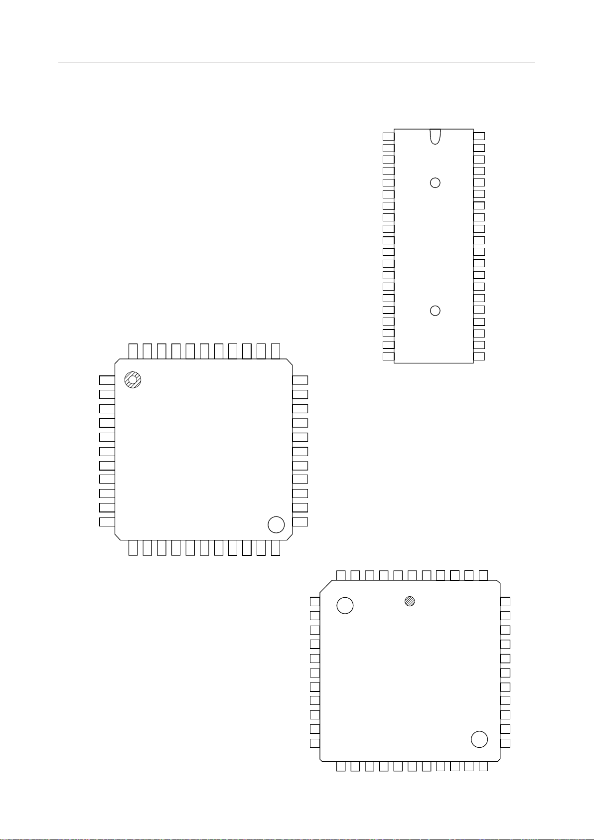
• 40-pin Plastic DIP (DIP40-P-600-2.54): (Product name: MSM82C37B-5RS)
• 44-pin Plastic QFJ (QFJ44-P-S650-1.27): (Product name: MSM82C37B-5VJS)
• 44-pin Plastic QFP (QFP44-P-910-0.80-2K): (Product name: MSM82C37B-5GS-2K)
1/33
¡ Semiconductor MSM82C37B-5RS/GS/VJS
PIN CONFIGURATION (TOP VIEW)
40 pin Plastic DIP
44 pin Plastic QFP
6A7
38
A5A4EOP
A
37
36
NC
MEMW
MEMR
IOW
IOR
NC
44
43
42
41
40
39
READY
ADSTB
RESET
DACK
DACK
1
HLDA
2
3
AEN
4
HRQ
5
NC
6
7
CS
8
CLK
9
10
2
11 DB
3
35
34
33
32
31
30
29
28
27
26
25
24
23
A
A
A
A
V
NC
DB
DB
DB
DB
1
IOR
2
IOW
3
MEMR
MEMW
READY
ADSTB
3
2
1
0
CC
0
1
2
3
4
4
5
NC
6
7
HLDA
8
9
AEN
10
HRQ
11
CS
12
CLK
13
RESET
DACK
14
2
DACK
15
3
DREQ
16
3
DREQ
17
2
DREQ
18
1
DREQ
19
0
20
GND
44 pin Plastic QFJ
40
39
38
37
36
35
34
33
32
31
30
29
28
27
26
25
24
23
22
21
A
7
A
6
A
5
A
4
EOP
A
3
A
2
A
1
A
0
V
CC
DB
0
DB
1
DB
2
DB
3
DB
4
DACK
DACK
DB
5
DB
6
DB
7
(+5 V)
0
1
12
13
3
DREQ
DREQ2DREQ1DREQ
14
15
16
17
18
19
20
21
0
GND
NC
DB
7
6DB5
DB
22
0
DACK1DACK
READY
HLDA
ADSTB
RESET
DACK2
NC
AEN
HRQ
CS
CLK
NC
10
11
12
13
14
15
16
17
7
NC
6
MEMW
MEMR
5
4
IOW
3
IORNCA
2
6A5A4
A
1
43
44
7
8
9
18
19
20
21
22
23
24
25
7
3
DACK
DREQ3DREQ2DREQ1DREQ
0
GND
DB
6DB5
DB
42
26
EOP
41
40
27
28
0
DACK1DACK
39
38
37
36
35
34
33
32
31
30
29
V
NC
A
A
A
A
DB
DB
DB
DB
DB
3
2
1
0
CC
0
1
2
3
4
2/33
¡ Semiconductor MSM82C37B-5RS/GS/VJS
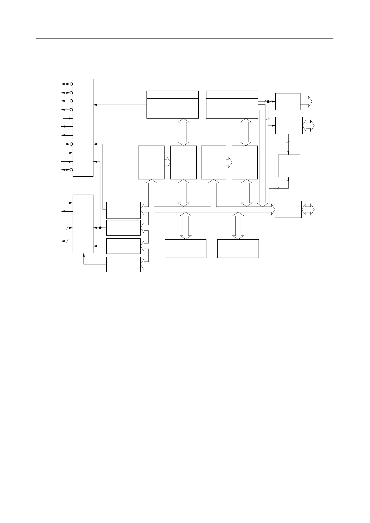
BLOCK DIAGRAM
IOR
MEMR
MEMW
READY
ADSTB
RESET
DREQ
DACK
IOW
AEN
CS
CLK
EOP
HLDA
HRQ
0 - 3
0 - 3
4
Judgment
4
Timing
Control
Circuit
Priority
Circuit
TC
(Terminal Count)
Mode
Register
¥
16)
(4
Command
Register (8)
Mark
Register (4)
Request
Register (4)
Decrementer
Temporary Word
Count Register (16)
Base Word
Count
Register
(4 ¥ 16)
16 Bit Bus
Current
Word
Count
Register
(4 ¥ 16)
Status
Register (8)
Incrementer/Decrementer
Temporary Address
Register (16)
16 Bit Bus
Base
Address
Register
(4 ¥ 16)
Internal Data Bus
Temporary
Register (8)
Current
Address
Register
(4 ¥ 16)
8 4
15
- A
8
A
Output
Buffer
4
Input/Output
Buffer
Command
Control
Circuit
2
D
0 - 1
Input/Output
Buffer
A
DB
4 - A7
A
0 - A3
0 - DB7
3/33
¡ Semiconductor MSM82C37B-5RS/GS/VJS
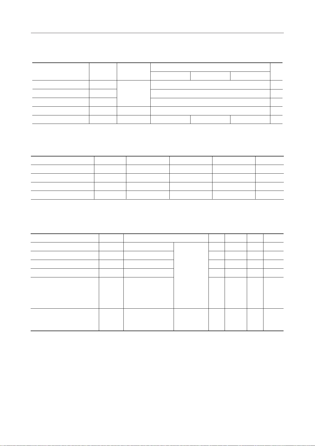
ABSOLUTE MAXIMUM RATINGS
Parameter Unit
Power Supply Voltage
Input Voltage
Output Voltage
Storage Temperature
Power Dissipation
Symbol
V
CC
V
IN
V
OUT
T
STG
P
D
Conditions
with respect
to GND
—
Ta = 25°C
MSM82C37B-5RS
1.0
MSM82C37B-5GS
–0.5 to +7
–0.5 to V
–0.5 to V
CC
CC
+0.5
+0.5
–55 to +150
0.7
MSM82C37B-5VJS
RECOMMENDED OPERATING CONDITIONS
Rating
Parameter UnitSymbol
Power Supply Voltage
Operating Temperature
"L" Input Voltage
"H" Input Voltage
Min.
V
CC
T
op
V
IL
T
IH
4.5
–40
–0.5
2.2
Typ.
5.0
+25
—
—
V
CC
Max.
5.5
+85
+0.8
+ 0.5
DC CHARACTERISTICS
1.0
V
V
V
°C
W
V
°C
V
V
Parameter Symbol
"L" Output Voltage V
"H" Output Voltage
Input Leak Current I
Output Leak Current I
Average Power Supply
Current during Operations
Power Supply Current
in Standby Mode
V
I
I
CCS
LO
CC
OL
OH
LI
Conditions
I
= 3.2 mA
OL
I
= –1.0 mA
OH
IN
OUT
£ V
£ V
CC
CC
0V £ V
0V £ V
Input frequency
5 MHz, when RESET
V
= 0 V/VCC,
IN
C
= 0 pF
L
= 0 V,
HLDA
V
= 0 V,
IL
V
= V
CC
IH
V
= 4.5 V
CC
to 5.5 V
Ta
= –40°C
to +85°C
Min.
—
3.7
–10
–10
—
—
Typ.
—
—
—
—
—
—
Max.
0.4
—
10
10
10
10
Unit
V
V
mA
mA
mA
mA
4/33

¡ Semiconductor MSM82C37B-5RS/GS/VJS
AC CHARACTERISTICS
DMA (Master) Mode
(Ta = –40 to +85°C, VCC = 4.5 to 5.5 V)
Symbol
Item
Min. Max. Unit
Comments
t
AEL
t
AET
t
AFAB
t
AFC
t
AFDB
t
AHR
t
AHS
t
AHW
Delay Time from CLK Falling Edge
up to AEN Leading Edge
Delay Time from CLK Rising Edge
up to AEN Trailing Edge
Delay Time from CLK Rising Edge
up to Address Floating Status
Delay Time from CLK Rising Edge
up to Read/Write Signal Floating Status
Delay Time from CLK Rising Edge
up to Data Bus Floating Status
Address Valid Hold Time
to Read Signal Trailing Edge
Data Valid Hold Time
to ADSTB Trailing Edge
Address Valid Hold Time
to Write Signal Trailing Edge
Delay Time from CLK Falling Edge
up to Active DACK
——200
——130
——90
——120
——170
tCY – 100 ——
30 ——
tCY – 50 ——
— (Note 3)170
ns
ns
ns
ns
ns
ns
ns
ns
ns
t
t
ASM
t
ASS
t
t
t
AK
CH
CL
CY
Delay Time from CLK Rising Edge
up to EOP Leading Edge
Delay Time from CLK Rising Edge
up to EOP Trailing Edge
Time from CLK Rising Edge
up to Address Valid
Data Set-up Time to ADSTB Trailing Edge
Clock High-level Time
Clock Low-level Time
CLK Cycle Time
— (Note 5)170
——170
——170
100 ——
68 (Note 6)—
68 (Note 6)—
200 ——
ns
ns
ns
ns
ns
ns
ns
5/33

¡ Semiconductor MSM82C37B-5RS/GS/VJS
DMA (Master) Mode (continued)
Symbol
t
DCL
t
DCTR
t
DCTW
t
DQ
t
EPS
t
EPW
t
FAAB
t
FAC
t
FADB
Item
Delay Time from CLK Rising Edge
to Read/Write Signal Leading Edge
Delay Time from CLK Rising Edge
to Read Signal Trailing Edge
Delay Time from CLK Rising Edge
to Write Signal Trailing Edge
Delay Time from CLK Rising Edge
to HRQ Valid
EOP Leading Edge Set-up Time to
CLK Falling Edge
EOP Pulse Width
Delay Time from CLK Rising Edge
to Address Valid
Time from CLK Rising Edge
up to Active Read/Write Signal
Delay Time from CLK Rising Edge
to Data Valid
Min. Max. Unit
— (Note 2)190
— (Note 2)190
— (Note 2)130
——120
40 ——
220
——170
——150
——200
ns
ns
ns
ns
ns
ns
ns
ns
ns
Comments
——
t
t
t
t
ODH
t
ODV
t
t
t
t
HS
IDH
IDS
QS
RH
RS
STL
HLDA Valid Set-up Time
to CLK Rising Edge
Input Data Hold Time
to MEMR Trailing Edge
Input Data Set-up
to MEMR Trailing Edge
Output Data Hold Time
to MEMW Trailing Edge
Time from Output Data Valid
to MEMW Trailing Edge
DREQ Set-up Time
to CLK Falling Edge
READY Hold Time
to CLK Falling Edge
READY Set-up Time
to CLK Falling Edge
Delay Time from CLK Rising Edge
to ADSTB Leading Edge
75 ——
0——
170 ——
10 ——
125 ——
0 (Note 3)—
20 ——
60 ——
——130
ns
ns
ns
ns
ns
ns
ns
ns
ns
t
STT
Delay Time from CLK Rising Edge
to ADSTB Trailing Edge
——90
ns
6/33

¡ Semiconductor MSM82C37B-5RS/GS/VJS
Slave Mode
Symbol
t
t
AW
t
CW
t
DW
t
t
RDE
t
RDF
t
RSTD
AR
RA
Time from Address Valid or
CS Leading Edge to IOR Leading Edge
Address Valid Set-up Time
to IOW Trailing Edge
CS Leading Edge Set-up Time
to IOW trailing edge
Data Valid Set-up Time
to IOW Trailing Edge
Address or CS Hold Time
to IOR Trailing Edge
Data Access Time
to IOR Leading Edge
Delay Time to Data Floating Status
from IOR Trailing Edge
Supply Power Leading Edge Set-up
time to RESET Trailing Edge
Item
(Ta = –40 to +85°C, VCC = 4.5 to 5.5 V)
Min. Max. Unit
50 ——
130 ——
130 ——
130 ——
0——
——140
0—70
500 ——
ns
ns
ns
ns
ns
ns
ns
ns
Comments
t
RSTS
t
RSTW
t
RW
t
WA
t
WC
t
WD
t
WWS
Time to First Active IOR or IOW
from RESET Trailing Edge
RESET Pulse Width
IOR Pulse Width
Address Hold Time
to IOW Trailing Edge
CS Trailing Edge Hold Time
to IOW Trailing Edge
Data Hold Time to IOW Trailing Edge
IOW Pulse Width
Notes: 1. Output load capacitance of 150 (pF).
2. IOW and MEMW pulse widths of tCY – 100 (ns) for normal writing, and 2tCY – 100
(ns) for extended writing. IOR and MEMR pulse widths of 2tCY – 50 (ns) for normal
timing, and tCY – 50 (ns) for compressed timing.
3. DREQ and DACK signal active level can be set to either low or high. In the timing
chart, the DREQ signal has been set to active-high, and the DACK signal to activelow.
4. When the CPU executes continuous read or write in programming mode, the
interval during which the read or write pulse becomes active must be set to at least
400 ns.
5. EOP is an open drain output. The value given is obtained when a 2.2 kW pull-up
resistance is connected to VCC.
6. Rise time and fall time are less than 10 ns.
7. Waveform measurement points for both input and output signals are 2.2 V for HIGH
and 0.8 V for LOW, unless otherwise noted.
2t
CY
300 ——
200 ——
20 ——
20 ——
30 ——
160 ——
ns
ns
ns
ns
ns
ns
ns
——
7/33
¡ Semiconductor MSM82C37B-5RS/GS/VJS
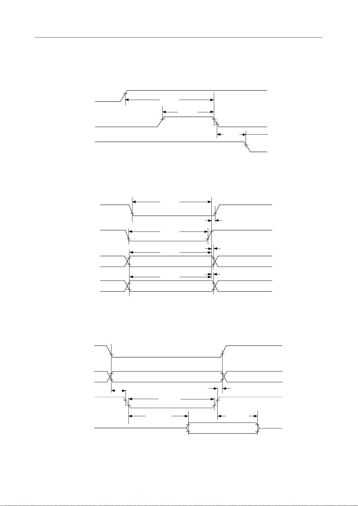
TIMING CHART
Reset Timing
V
CC
RESET
IOR, IOW
Slave Mode Write Timing
CS
t
RSTD
t
CW
t
RSTW
t
RSTS
t
WC
IOW
A
- A
0
3
DB0 - DB
7
Slave Mode Read Timing
CS
- A
A
0
3
IOR
t
WWS
t
t
AW
WA
Input Valid Address
t
t
DW
WD
Input Valid Data
Input Valid Address
t
AR
t
RW
t
RA
DB
- DB
0
t
RDE
7
Output Valid Data
t
RDF
8/33
¡ Semiconductor MSM82C37B-5RS/GS/VJS
(Input)
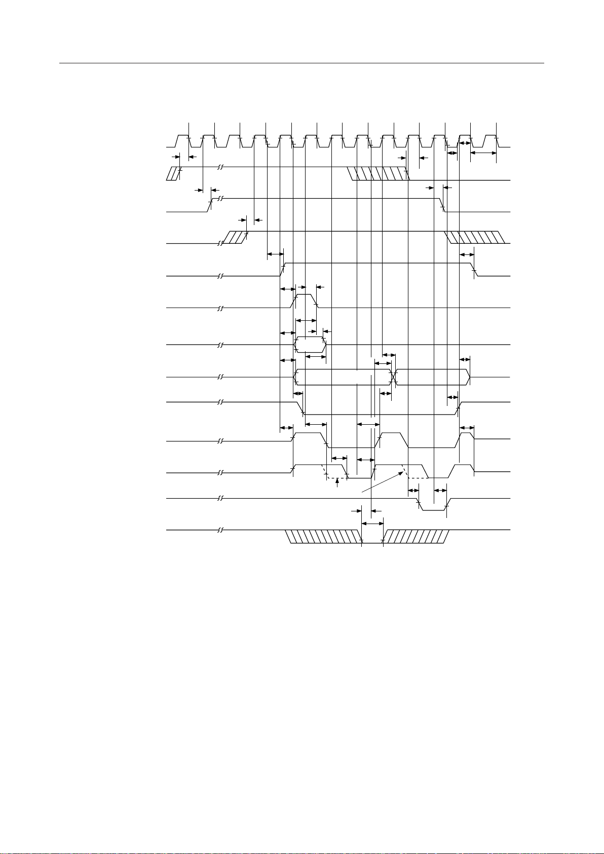
DMA Transfer Timing
CLK
DREQ
HRQ
HLDA
AEN
ADSTB
- DB
DB
0
A0 - A
DACK
IOR, MEMR
SI SI S0S0S1S
t
QS
t
DQ
t
HS
t
7
7
AEL
t
t
t
STL
FADB
FAAB
S3S
2
t
STT
t
ASS
t
AHS
A8 - A
15
t
AFDB
A0 - A
t
AK
t
FAC
DCL
t
DCL
t
S2S3S
4
t
ASM
t
AHW
7
t
DCTR
t
DCTW
t
AHR
t
QS
t
DQ
A0 - A
4
t
AK
t
CL
7
SI SI
t
CH
t
CY
t
AET
t
AFAB
t
AFC
IOW, MEMW
Internal EOP
(Output)
External EOP
(Extended Write)
t
EPS
t
EPW
t
t
AK
AK
9/33
¡ Semiconductor MSM82C37B-5RS/GS/VJS
(Input)
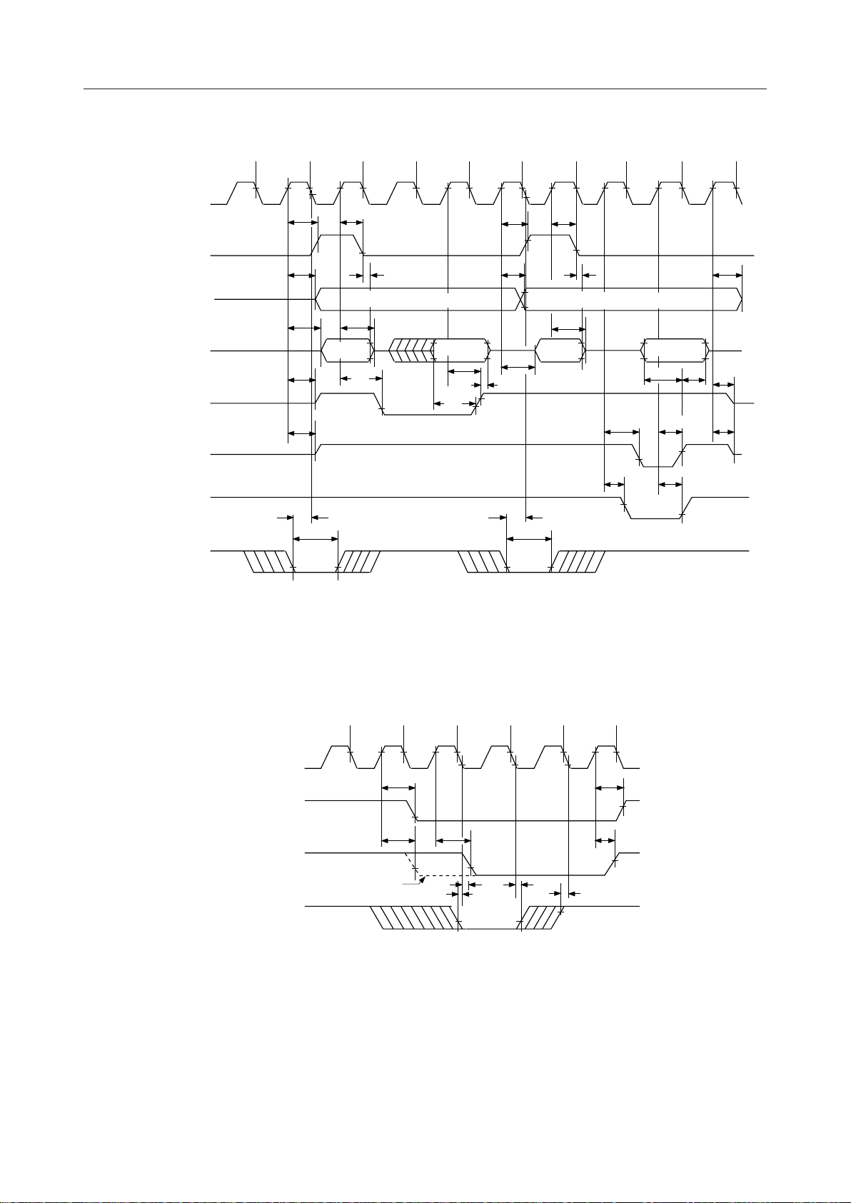
Memory to Memory Transfer Timing
CLK
ADSTB
A0 - A
DB
- DB
0
MEMR
MEMW
Internal EOP
(Output)
External EOP
S
S
0
t
FAAB
7
t
FADB
7
t
EPS
11
S
12
t
STL
t
A8 - A
t
FAC
t
FAC
t
EPW
S
13
STT
t
AHS
Valid Address A
t
AFDB
15
t
DCL
S
14
0 - 7
Data Input
t
DCTR
t
IDS
S
t
EPS
S
21
t
t
t
IDH
STL
ASM
t
FADB
t
22
A8 - A
EPW
S
23
t
STT
t
AHS
Valid Address A
t
AFDB
15
S
24
SI
t
AFAB
0 - 7
Data Output
t
ODVtODH
t
t
DCL
t
AK
DCTW
t
AK
t
AFC
t
AFC
Ready Timing
CLK
IOR, MEMR
IOW, MEMW
READY
S
2
(Extended Write)
S
t
DCL
t
DCL
t
RS
S
3
W
t
DCL
t
RH
S
t
S
W
RH
4
t
DCTR
t
DCTW
t
RS
10/33
¡ Semiconductor MSM82C37B-5RS/GS/VJS
(Input)
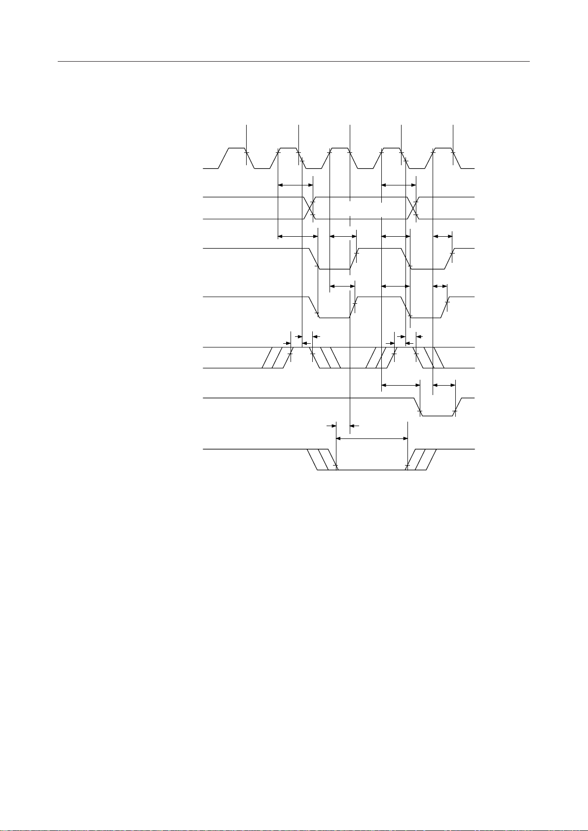
Compressed Transfer Timing
CLK
A
- A
0
IOR, MEMR
IOW, MEMW
READY
Internal EOP
(Output)
S
2
t
ASM
7
t
t
RS
DCL
S
4
t
RH
t
EPS
Valid Address
t
DCTR
t
DCTW
t
S
EPW
2
t
ASM
t
DCL
t
DCL
t
RS
S
4
t
DCTR
t
DCTW
t
RH
t
AK
t
AK
External EOP
11/33
 Loading...