E2O0014-27-X2
¡ Semiconductor MSM81C55-5RS/GS/JS
¡ Semiconductor
This version: Jan. 1998
Previous version: Aug. 1996
MSM81C55-5RS/GS/JS
2048-Bit CMOS STATIC RAM WITH I/O PORTS AND TIMER
GENERAL DESCRIPTION
The MSM81C55-5 has a 2k-bit static RAM (256 bytes) with parallel I/O ports and a timer. It uses
silicon gate CMOS technology and consumes a standby current of 100 micro ampere, maximum,
while the chip is not selected. Featureing a maximum access time of 400 ns, the MSM81C55-5
can be used in an MSM80C85AH system without using wait states. The parallel I/O consists
of two 8-bit ports and one 6-bit port (both general purpose).
The MSM81C55-5 also contains a 14-bit programmable counter/timer which may be used for
sequence-wave generation or terminal count-pulsing.
FEATURES
• High speed and low power achieved with silicon gate CMOS technology
• 256 words x 8bits RAM
• Single power supply, 3 to 6 V
• Completely static operation
• On-chip address latch
• 8-bit programmable I/O ports (port A and B)
• TTL Compatible
• RAM data hold characteristic at 2 V
• 6-bit programmable I/O port (port C)
• 14-bit programmable binary counter/timer
• Multiplexed address/data bus
• Direct interface with MSM80C85AH
• 40-pin Plastic DIP (DIP40-P-600-2.54): (Product name: MSM81C55-5RS)
• 44-pin Plastic QFJ (QFJ44-P-S650-1.27): (Product name: MSM81C55-5JS)
• 44-pin Plastic QFP (QFP44-P-910-0.80-2K): (Product name: MSM81C55-5GS-2K)
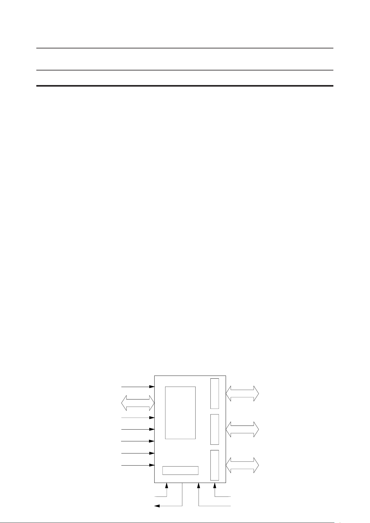
FUNCTIONAL BLOCK DIAGRAM
Port A
8
Port B
8
PA
PB
0 - 7
0 - 7
AD
IO/M
0 - 7
CE
ALE
A
256 ¥ 8
Static
RAM
B
RD
WR
RESET
TIMER IN
TIMER OUT
Timer
Port C
C
6
V
CC
GND (0 V)
(+5 V)
PC
0 - 5
1/19
¡ Semiconductor MSM81C55-5RS/GS/JS
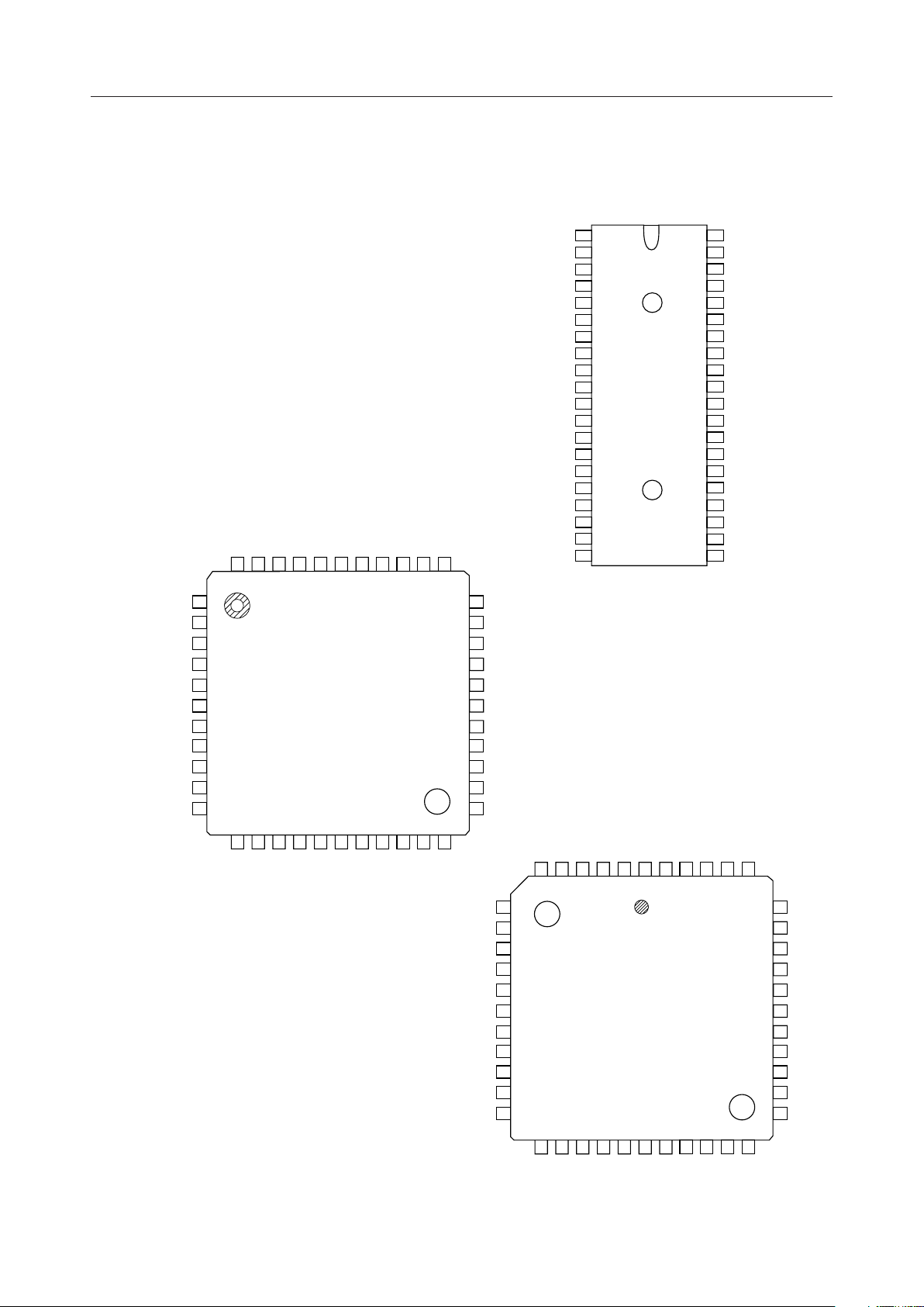
PIN CONFIGURATION (TOP VIEW)
40 pin Plastic DIP
TIMEROUT
IO/M
RD
WR
ALE
AD
AD
AD
AD
NC
44 pin Plastic QFP
5
RESET
TIMER IN
PC
PC4PC3V
4443424140
1
2
CE
3
4
5
6
7
0
8
1
9
2
10
3
11 PA
CC
39
2PC1PC0PB7
NC
PC
37
38
363534
1
PC
3
2
PC
4
TIMER IN
TIMER OUT
33
PB
6
PB
32
5
PB
31
4
PB
30
3
PB
29
2
PB
28
1
PB
27
0
26
PA
7
PA
25
6
PA
24
5
23
4
3
4
RESET
5
PC
5
6
7
IO/M
8
CE
9
RD
10
WR
11
ALE
AD
12
0
AD
13
1
AD
14
2
AD
15
3
AD
16
4
AD
17
5
AD
18
6
AD
19
7
20
GND
44 pin Plastic QFJ
40
V
CC
39
PC
2
38
PC
1
37
PC
0
PB
36
7
35
PB
6
34
PB
5
33
PB
4
32
PB
3
31
PB
2
30
PB
1
29
PB
0
28
PA
7
27
PA
6
26
PA
5
25
PA
4
24
PA
3
23
PA
2
22
PA
1
21
PA
0
12131415161718
4AD5
AD
AD6AD7GND
CC
V
192021
0
PA
1PA2PA3
PA
22
NC
TIMER OUT
IO/M
RD
WR
NC
ALE
AD
AD
AD
AD
PC
6
5
RESET
5
TIMER IN
PC4PC3NC
4
3
2
1
2PC1PC0PB7
CC
V
PC
43
44
424140
7
8
CE
9
10
11
12
13
14
0
15
1
16
2
17 PA
3
18192021222324
AD
4
NC
7
AD5AD6AD
GND
252627
0
1PA2PA3PA4
PA
PA
28
39
38
37
36
35
34
33
32
31
30
29
PB
6
PB
5
PB
4
PB
3
PB
2
NC
PB
1
PB
0
PA
7
PA
6
5
2/19
¡ Semiconductor MSM81C55-5RS/GS/JS
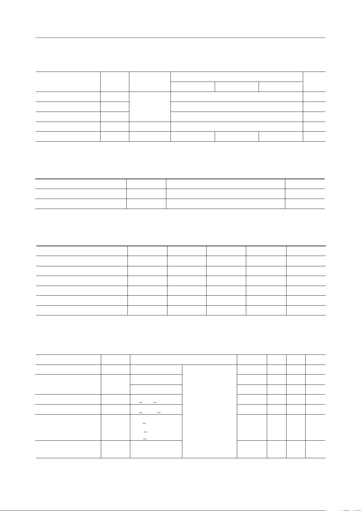
ABSOLUTE MAXIMUM RATING
Parameter Unit
Power Supply Voltage
Input Voltage
Output Voltage
Storage Temperature
Power Dissipation
Symbol
V
CC
V
IN
V
OUT
T
STG
P
D
Conditions
Referenced
to GND
—
Ta = 25°C
MSM81C55-5RS
MSM81C55-5GS MSM81C55-5JS
–0.5 to +7
–0.5 to V
–0.5 to V
CC
CC
+0.5
+0.5
–55 to +150
0.7
1.01.0
OPERATING CONDITION
Rating
Parameter UnitSymbol
Power Supply Voltage
Operating Temperature
V
CC
T
OP
Range
3 to 6
–40 to +85
RECOMMENDED OPERATING CONDITIONS
Parameter UnitSymbol
Power Supply Voltage (81C55)
Operating Temperature (81C55)
"L" Level Input V
"H" Level Input
Supply Voltage (81C55-5)
Operating Temperature (81C55-5)
Min.
V
CC
T
OP
IL
V
IH
V
CC
V
OP
4.5
–40
–0.3
2.2
Typ.
5V
+25
—
—
54.75 5.25
+25–40 +70
Max.
+85
+0.8
V
CC
5.5
+0.3
V
V
V
°C
W
V
°C
°C
V
V
V
°C
DC CHARACTERISTICS
Parameter Unit
"L" Level Output Voltage
"H" Level Output Voltage
Input Leak Current
Output Leak Current
Symbol
V
OL
V
OH
I
LI
I
LO
I
= 2 mA
OL
I
= –400 mA
OH
I
= –40 mA
OH
0 £ V
0 £ V
IN
OUT
CE ≥ V
Standby Current
Mean Operating
Current
I
CCS
I
CC
≥ V
V
IH
V
£ –0.2 V
IL
Memory cycle
time: 1 ms
£ V
CC
CC
£ V
–0.2 V
–0.2 V
Condition
CC
CC
= 4.5 V to 5.5 V
V
CC
= –40°C to 85°C
Ta
Min.
—
2.4
4.2
–10
–10
—
—
Typ. Max.
— 0.45 V
—— V
—— V
—10mA
—10mA
0.1 100 mA
—5mA
3/19
¡ Semiconductor MSM81C55-5RS/GS/JS
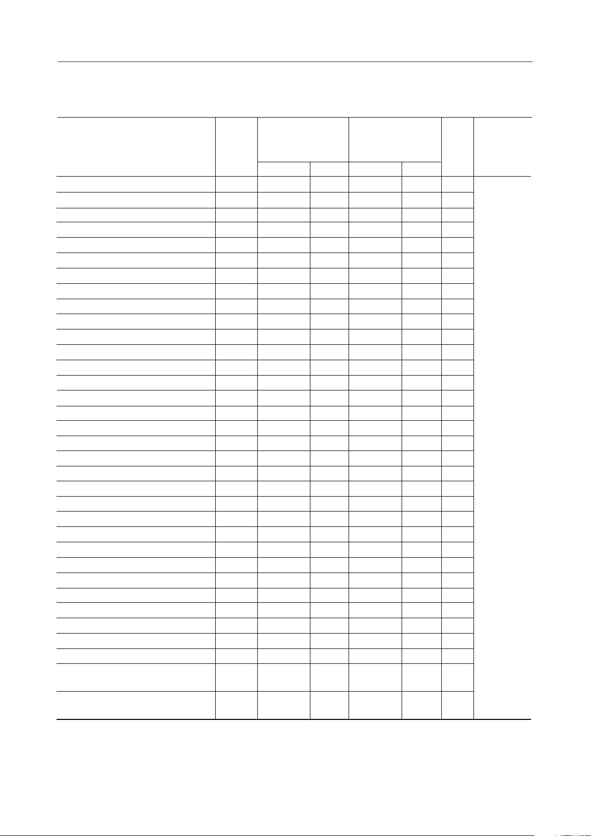
AC CHARACTERISTICS
V
= 4.75 V to 5.25 V,
CC
Ta = –40 to +70°C
80C85AH 5MHz I/F
Parameter
V
= 4.5 V to 5.5 V,
CC
Symbol Unit Remarks
Ta = –40 to +80°C
80C85AH 3MHz I/F
Min.
Address/latch Setup Time
Latch/address Holt Time
Latch/read (write) Delay Time
Read/output Delay Time
Address/output Delay Time
Latch Width
Read/data Bus Floating Time
Read (write)/latch Delay Time
Read (write) Width
Data In/write Setup Time
Write/data-in Hold Time
Recovery Time
Write/port Output Delay Time
Port Input/read Setup Time Load capaciRead/port Input Hold Time
Strobe/buffer Full Delay Time
Strobe Width
Strobe/buffer Empty Delay Time
Strobe/interrupt-on Delay Time
Read/interrupt-off Delay Time
Port Input/strobe Setup Time
Strobe/port-input Hold Time
Strobe/buffer-empty Delay Time
Write/buffer-full Delay Time
Write/interrupt-off Delay Time
Time Output Delay Time Low
Time Output Delay Time High
Read/data Buse Enable Delay Time
Timer Cycle Time
Timer Input Rise and Fall Times
Timer Input Low Level Time
Timer Input High Level Time
WRITE to TIMER-IN
for writes which start counting
TIMER-IN to WRITE
for writes which start counting
t
t
t
t
RD
t
AD
t
t
RDF
t
t
CC
t
DW
t
WD
t
RV
t
WP
t
PR
t
RP
t
SBF
t
SS
t
RBE
t
t
RDI
t
PSS
t
PHS
t
SBE
t
WBF
t
WI
t
t
TH
t
RDE
t
CYC
tr, t
t
t
t
WT
t
TW
AL
LA
LC
LL
CL
SI
TL
f
1
2
50
30
100
—
—
100
0
20
250
150
0
300
—
70
50
—
200
—
—
—
50
120
—
—
—
—
—
10
320
—
80
120
200
0
Max.
—
—
—
170
400
—
100
—
—
—
—
—
400
—
—
400
—
400
400
400
—
—
400
400
400
400
400
—
—
80
—
—
—
—
37 —
30 —
40 —
— 140
— 330
70 —
080
20 —
200 —
100 —
25 —
200 —
— 300
50 —
10 —
— 300
150 —
— 300
— 300
— 300
20 —
100 —
— 300
— 300
— 300
— 300
— 300
10 —
320 —
—80
40 —
70 —
200 —
0—
Max.Min.
ns
ns
ns
ns
ns
ns
ns
ns
ns
ns
ns
ns
ns
ns
tance: 150 pF
ns
ns
ns
ns
ns
ns
ns
ns
ns
ns
ns
ns
ns
ns
ns
ns
ns
ns
ns
ns
ns
Note: Timings are measured wth VL = 0.8 V and VH = 2.2 V for both input and output.
4/19
¡ Semiconductor MSM81C55-5RS/GS/JS
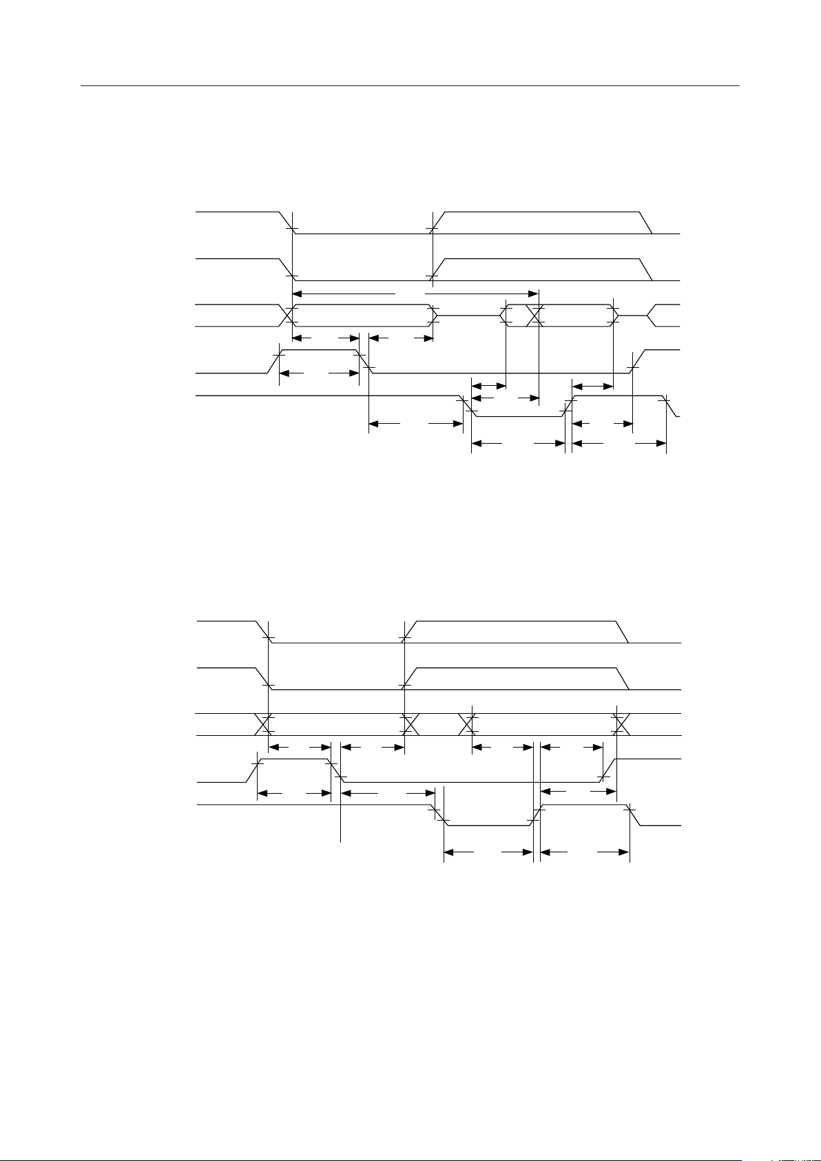
TIMING DIAGRAM
Read Cycle
CE
IO/M
t
AD
t
CC
Data Valid
t
RDF
t
CL
t
RV
AD
0 - 7
ALE
RD
t
LL
t
AL
Address
t
LA
t
RDE
t
RD
t
LC
Write Cycle
IO/M
AD
CE
0 - 7
ALE
WR
t
t
LL
AL
Address
Data Valid
t
LA
t
LC
t
DW
t
CC
t
CL
t
WD
t
RV
5/19
¡ Semiconductor MSM81C55-5RS/GS/JS
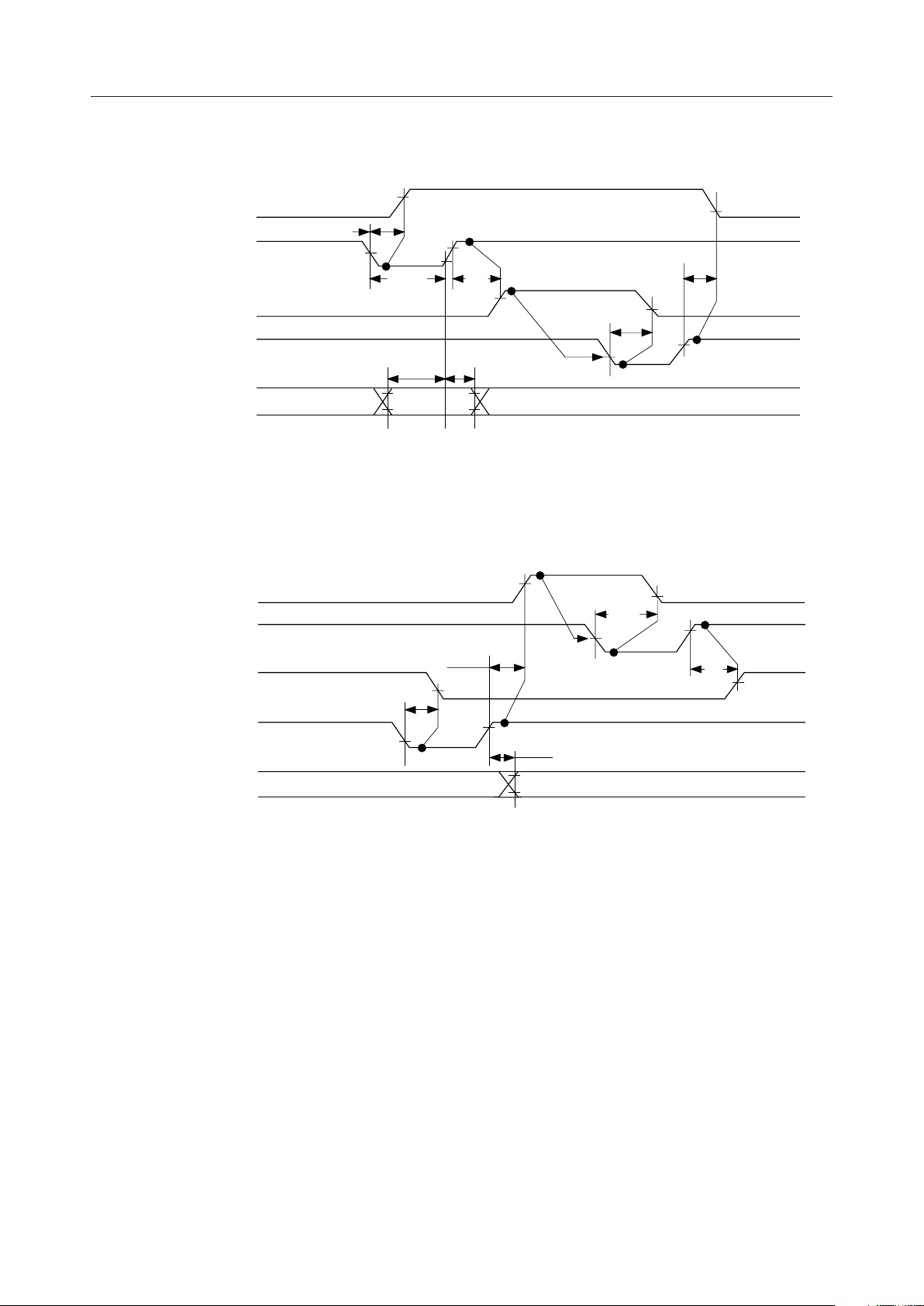
Strobe Input Mode
BF
t
SBF
STROBE
INTR
t
SS
t
SI
t
RDI
t
RBE
RD
Input Data
From Port
Strobe Output Mode
BF
STROBE
INTR
WR
Output Data
To Port
t
PSS
t
WI
t
PHS
t
WBF
t
WP
t
SBE
t
SI
6/19
 Loading...