


E2O0010-27-X2
¡ Semiconductor MSM80C86A-10RS/GS/JS
¡ Semiconductor
This version: Jan. 1998
Previous version: Aug. 1996
MSM80C86A-10RS/GS/JS
16-Bit CMOS MICROPROCESSOR
GENERAL DESCRIPTION
The MSM80C86A-10 is complete 16-bit CPUs implemented in Silicon Gate CMOS technology.
They are designed with same processing speed as the NMOS 8086-1 but have considerably less
power consumption. It is directly compatible with MSM80C88A-10 software and MSM80C85AH
hardware and peripherals.
FEATURES
• 1 Mbyte Direct Addressable Memory Space
• Internal 14-word by 16-bit Register Set
• 24-Operand Addressing Modes
• Bit, Byte, Word and String Operations
• 8 and 16-bit Signed and Unsigned Arithmetic Operation
• From DC to 10 MHz Clock Rate (Note)
• Low Power Dissipation 10 mA/MHz
• Bus Hold Circuitry Eliminated Pull-up Resistors
• 40-pin Plastic DIP (DIP40-P-600-2.54): (Product name: MSM80C86A-10RS)
• 44-pin Plastic QFJ (QFJ44-P-S650-1.27): (Product name: MSM80C86A-10JS)
• 56-pin Plastic QFP (QFP56-P-1519-1.00-K): (Product name: MSM80C86A-10GS-K)
(Note) 10 MHz Spec is not compatible with Intel 8086-1 Spec.
1/37
¡ Semiconductor MSM80C86A-10RS/GS/JS
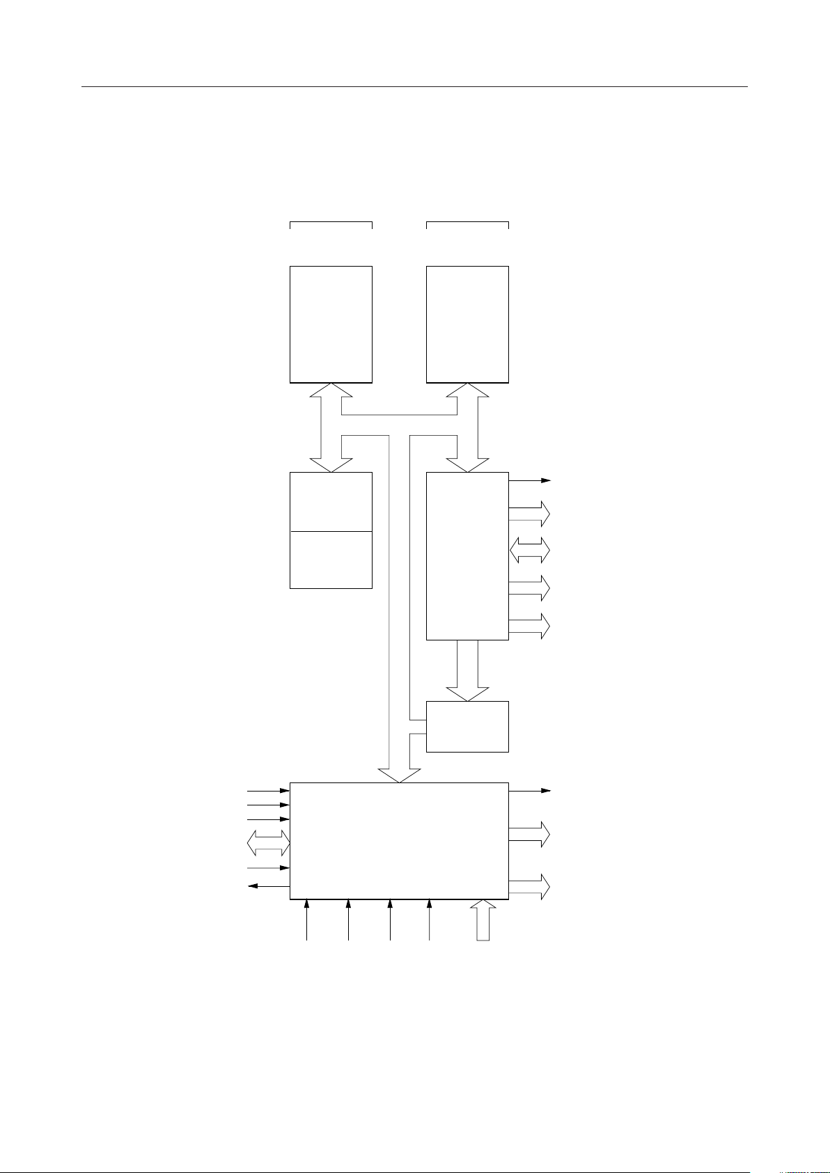
CIRCUIT CONFIGURATION
Exeuction Unit
Register File
Data
Pointer
and
Index
Registers
(8 Words)
16-Bit ALU
Flags
Bus Interface Unit
Relocation
Register File
Segment
Registers
and
Instruction
Pointer
(5 Words)
Bus
Interface
Unit
BHE/S
7
A
19/S6
.
4
16
4
.
.
A16/S
3
AD15 - AD
INTA, RD, WR, M/IO
0
TEST
INTR
RQ/GT
HOLD
HLDA
NMI
0, 1
3
DT/R, DEN, ALE
6Byte
Instruction
Queue
LOCK
2
Control & Timing
MN/MXREADYRESETCLK
3
GND
V
2
3
CC
, QS
QS
0
S2, S1, S
1
0
2/37
¡ Semiconductor MSM80C86A-10RS/GS/JS
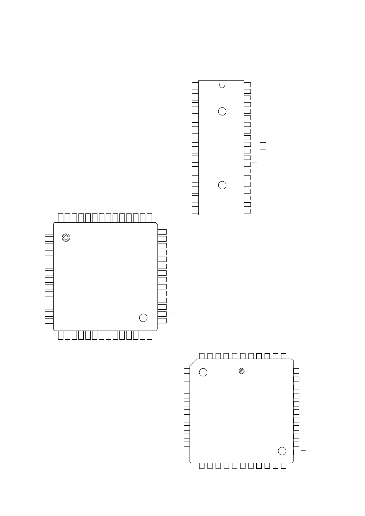
PIN CONFIGURATION (TOP VIEW)
40 pin Plastic DIP
AD
AD
AD
AD
AD
AD
AD
AD
AD
AD
AD
NC
NC
NC
1
GND
2
AD
14
3
AD
13
4
AD
12
5
AD
11
6
AD
10
7
AD
9
8
AD
8
9
AD
7
10
AD
6
11
AD
5
12
AD
4
13
AD
3
14
AD
2
15
AD
19/S6
(M/IO)
2
(DT/R)
1
(DEN)
0
AD
NMI
INTR
CLK
GND
7
(HOLD)
0
1
16
0
17
18
19
20
56 pin Plastic QFP
3
4
5
/S
/S
11
12
13
AD
56
AD
55
AD
54
AD
14
53
52NC51
GND50NC49V
CC
15
CC
V
AD
48
47NC46
1
2
10
3
9
4
8
5
7
6
6
7
8
9
5
10
4
11
3
12
2
13
1
14
0
/S
16
17
18
A
A
A
45
44
43
NC
42
A
41
BHE/S
40
MN/MX
39
RD
38
RQ/GT
37
NC
36
NC
35
NC
34
33
RQ/GT1(HLDA)
32
LOCK(WR)
31
S
30
S
29
S
40
39
38
37
36
35
34
33
32
31
30
29
28
27
26
25
24
23
22
21
V
CC
AD
15
A16/S
3
A17/S
4
A18/S
5
A19/S
6
BHE/S
7
MN/MX
RD
(HOLD)
RQ/GT
0
(HLDA)
RQ/GT
1
LOCK(WR)
(M/IO)
S
2
(DT/R)
S
1
(DEN)
S
0
(ALE)
QS
0
(INTA)
QS
1
TEST
READY
RESET
15
NMI
16
INTR
17
CLK
18NC19NC20
GND
21
CC
V
22NC23NC24
25
RESET
READY
26
TEST
27
(INTA)
QS
28
(ALE)
0
1
QS
7
AD
10
AD
8
9
AD
9
8
AD
10
7
AD
11
6
AD
12
5
AD
13
4
14
AD
3
15
AD
2
16
AD
1
AD
17 S
0
44 pin Plastic QFJ
11AD12AD13AD14
AD
6
5
4
3
18192021222324
NC
NM1
INTR
CLK
GND
2
GND
NC
1
NC
V
CC
AD
43
44
252627
RESET
3
/S
15
16
A
424140
READY
TEST
4
/S
17
A
)
INTA(QS
1
5
/S
18
A
28
)
0
ALE(QS
39
NC
38
A
BHE/S
37
MN/MX
36
RD
35
RQ/GT
34
RQ/GT
33
32
LOCK(WR)
31
S
S
30
29
19/S6
(M/IO)
2
(DT/R)
1
(DEN)
0
7
(HOLD)
0
(HLDA)
1
3/37
¡ Semiconductor MSM80C86A-10RS/GS/JS
ABSOLUTE MAXIMUM RATINGS
Rating
CC
IN
D
Conditions
With respect
to GND
—
Ta = 25°C
MSM80C86A-10RS
1.0
MSM80C86A-10GS
–0.5 to + 7
–0.5 to V
–0.5 to V
CC
CC
+0.5
+0.5
–65 to +150
MSM80C86A-10JS
0.7
Parameter Unit
Power Supply Voltage
Input Voltage
Output Voltage
Storage Temperature
Power Dissipation
Symbol
V
V
V
OUT
T
STG
P
OPERATING RANGE
Parameter UnitSymbol
Power Supply Voltage
Operating Temperature
V
CC
T
op
Range
4.75 to 5.25
0 to +70
RECOMMENDED OPERATING CONDITIONS
Parameter UnitSymbol
Power Supply Voltage
Operating Temperature
"L" Input Voltage V
"H" Input Voltage
V
CC
T
OP
IL
*1 —
V
IH
*2 —2.0 V
Min.
V
CC
4.75
0
–0.5
–0.8
Typ.
5.0 V
+25
—
Max.
5.25
+70
+0.8
V
CC
CC
+0.5
+0.5
V
V
V
°C
W
V
°C
°C
V
V
V
*1 Only CLK
*2 Except CLK
4/37
¡ Semiconductor MSM80C86A-10RS/GS/JS
DC CHARACTERISTICS
(VCC = 4.5 to 5.5 V, Ta = –40°C to +85°C)
Parameter UnitSymbol Min.
"L" Output Voltage V
"H" Output Voltage V
Input Leak Current I
Output Leak Current I
Input Leakage Current
(Bus Hold Low)
Input Leakage Current
(Bus Hold High)
Bus Hold Low Overdrive
Bus Hold High Overdrive
I
I
Operating Power
Supply Current
Standby Power
Supply Current
OL
OH
LI
LO
I
BHL
I
BHH
BHLO
BHHO
I
CC
I
CCS
V
—
3.0
CC
–1.0
–10
—
—
Typ.
—
–0.4
—
—
—
—
—
—
—
—
Max.
0.4
V
——V
+1.0
+10
400
–400
600
–600
10
500
mA
mA
mA50
mA–50
mA—
mA—
mA/MHz
mA
Conditions
= 2.5 mA
I
OL
I
= –2.5 mA
OH
I
= –100 mA
OH
0 £ V
VO = V
V
IN
V
IN
V
IL
V
IH
V
CC
Outputs Unloaded
V
= V
IN
£ V
IN
or GND
CC
= 0.8 V
*3
= 3.0 V
*4
*5
*6
= GND
= VCC
= 5.5 V
or GND
CC
CC
Input Capacitance C
Output Capacitance C
I/O Capacitance C
IN
OUT
I/O
—
—
—
—
—
10
15
20
pF
pF
pF
*7
*7
*7—
*3 Test condition is to lower VIN to GND and then raise VIN to 0.8 V on pins 2-16, and 35-39.
*4 Test condition is to raise VIN to VCC and then lower VIN to 3.0 V on pins 2-16, 26-32, and 34-
39.
*5 An external driver must source at least I
*6 An external driver must sink at least I
BHHO
to switch this node from LOW to HIGH.
BHLO
to switch this node from HIGH to LOW.
*7 Test Conditions: a) Freq = 1 MHz.
b) Unmeasured Pins at GND.
c) VIN at 5.0 V or GND.
5/37
¡ Semiconductor MSM80C86A-10RS/GS/JS
AC CHARACTERISTICS
Minimum Mode System
Timing Requirements
Parameter
CLK Cycle Period
CLK Low Time
CLK High Time
CLK Rise Time
(From 1.0 V to 3.5 V)
CLK Fall Time
(From 3.5 V to 1.0 V)
Data in Setup Time
Data in Hold Time
RDY Setup Time into
MSM 82C84A-2 (See Notes 1, 2)
RDY Hold Time into MSM 82C84A-2
(See Notes 1, 2)
READY Setup Time into
MSM80C86A-2
READY Hold Time into MSM80C86A-10
READY inactive to CLK
(See Note 3)
HOLD Setup Time
INTR, NMI, TEST Setup Time
(See Note 2)
Input Rise Time (Except CLK)
(From 0.8 V to 2.0 V)
Input Fall Time (Except CLK)
(From 2.0 V to 0.8 V)
Symbol
t
CLCL
t
CLCH
t
CHCL
t
CH1CH2
t
CL2CL1
t
DVCL
t
CLDX
t
R1VCL
t
CLR1X
t
RYHCH
t
CHRYX
t
RYLCL
t
HVCH
t
INVCH
t
ILIH
t
IHIL
5 MHz Spec.
V
= 4.5 V to 5.5 V
CC
Ta = –40 to +85°C
Min.
200
118
69
—
—
30
10
35
0
118
30
–8
35
30
—
—
Max.
DC
—
—
10
10
—
—
—
—
—
—
—
—
—
15
15
8 MHz Spec.
V
= 4.75 V to 5.25 V
CC
Ta = 0 to +70°C
Max.Min.
125 DC
68 —
44 —
20 —
10 —
68 —
20 —
10 MHz Spec.
V
= 4.75 V to 5.25 V
CC
Ta = 0 to +70°C
Max.Min.
100 DC ns
46 — ns
44 — ns
—10ns—10
—10ns—10
20 — ns
10 — ns
35 — ns35 —
0—ns0—
46 — ns
20 — ns
–8 — ns–8 —
20 — ns20 —
15 — ns15 —
—15ns—15
—15ns—15
Unit
6/37

¡ Semiconductor MSM80C86A-10RS/GS/JS
Timing Responses
Parameter
Address Valid Delay
Address Hold Time
Address Float Delay
ALE Width
ALE Active Delay
ALE Inactive Delay
Address Hold Time to ALE Inactive
Data Valid Delay
Data Hold Time
Data Hold Time after WR
Control Active Delay 1
Control Active Delay 2
Control Inactive Delay
Address Float to RD Active
RD Active Delay
RD Inactive Delay
RD Inactive to Next Address Active
HLDA Valid Delay
RD Width
WR Width
Address Valid to ALE Low
Ouput Rise Time (From 0.8 V to 2.0 V)
Output Fall Time (From 2.0 V to 0.8 V)
Symbol
t
CLAV
t
CLAX
t
CLAZ
t
LHLL
t
CLLH
t
CHLL
t
LLAX
t
CLDV
t
CHDX
t
WHDX
t
CVCTV
t
CHCTV
t
CVCTX
t
AZRL
t
CLRL
t
CLRH
t
RHAV
t
CLHAV
t
RLRH
t
WLWH
t
AVAL
t
OLOH
t
OHOL
5 MHz Spec.
V
= 4.5 V to 5.5 V
CC
Ta = -40 to +85°C
Min.
10
10
t
CLAX
t
CLCH
—
—
t
CLCH
10
10
t
CLCH
10
10
10
0
10
10
t
CLC
10
2t
CLCL
2t
CLCL
t
CLCH
—
—
-20
-10
-30
-45
-60
-60
-75
Max.
110
—
80
—
80
85
—
110
—
—
110
110
110
—
165
150
—
160
—
—
—
15
15
8 MHz Spec.
V
= 4.75 V to 5.25 V
CC
Ta = 0 to +70°C
Max.Min.
10 60
10 —
t
CLAX
-10 —
CLCH
-10 —
CLCH
-30 —
CLCH
10 80
t
-40 —
CLCH
10 100
-50 —
CLCL
-40 —
CLCL
-40 —
CLCH
10 MHz Spec.
V
Ta = 0 to +70°C
50
= 4.75 V to 5.25 V
CC
Max.Min.
10 60 ns
10 — ns
t
t
CLCH
CLAX
-10 — nst
50 ns
—40ns—50
—45ns—55
t
CLCH
-10
—nst
10 60 ns10 60
10 — ns10 —
t
-25 — nst
CLCH
10 55 ns10 70
10 50 ns10 60
10 55 ns10 70
0—ns0—
10 70 ns10 100
10 60 ns
t
-35 — ns
CLCL
10 60 ns
2t
-40 — ns2t
CLCL
2t
-35 — ns2t
CLCL
t
-35 — nst
CLCH
—15ns—15
—15ns—15
Unit
Notes: 1. Signal at MSM82C84A-2 or MSM82C88-2 are shown for reference only.
2. Setup requirement for asynchronous signal only to guarantee recognition at next
CLK.
3. Applies only to T2 state. (8 ns into T3)
7/37
¡ Semiconductor MSM80C86A-10RS/GS/JS
Maximum Mode System (Using MSM82C88-2 Bus Controller)
Timing Requirements
Parameter
CLK Cycle Period
CLK Low Time
CLK High Time
CLK Rise Time
(From 1.0 V to 3.5 V)
CLK Fall Time
(From 3.5 V to 1.0 V)
Data in Setup Time
Data in Hold Time
RDY Setup Time into
MSM 82C84A-2 (See Notes 1, 2)
RDY Hold Time into MSM 82C84A-2
(See Notes 1, 2)
READY Setup Time into
MSM80C86A-10
READY Hold Time into MSM80C86A-10
READY inactive to CLK
(See Note 3)
Setup Time for Recognition (NMI,
INTR, TEST) (See Note 2)
RQ/GT Setup Time
RQ Hold Time into MSM80C86A-10
Input Rise Time (Except CLK)
(From 0.8 V to 2.0 V)
Input Fall Time (Except CLK)
(From 2.0 V to 0.8 V)
Symbol
t
CLCL
t
CLCH
t
CHCL
t
CH1CH2
t
CL2CL1
t
DVCL
t
CLDX
t
R1VCL
t
CLR1X
t
RYHCH
t
CHRYX
t
RYLCL
t
INVCH
t
GVCH
t
CHGX
t
ILIH
t
IHIL
5 MHz Spec.
V
= 4.5 V to 5.5 V
CC
Ta = –40 to +85°C
Min.
200
118
69
—
—
30
10
35
0
118
30
–8
30
30
40
—
—
Max.
DC
—
—
10
10
—
—
—
—
—
—
—
—
—
—
15
15
8 MHz Spec.
V
= 4.75 V to 5.25 V
CC
Ta = 0 to +70°C
Max.Min.
125 DC
68 —
44 —
20 —
10 —
68 —
20 —
10 MHz Spec.
V
= 4.75 V to 5.25 V
CC
Ta = 0 to +70°C
Max.Min.
100 DC ns
46 — ns
44 — ns
—10ns—10
—10ns—10
20 — ns
10 — ns
35 — ns35 —
0—ns0—
46 — ns
20 — ns
–8 — ns–8 —
15 — ns15 —
15 — ns15 —
20 — ns30 —
—15ns—15
—15ns—15
Unit
8/37
¡ Semiconductor MSM80C86A-10RS/GS/JS
Timing Responses
50
—
—
10 MHz Spec.
= 4.75 V to 5.25 V
V
CC
Ta = 0 to +70°C
Unit
Max.Min.
535ns
545ns
—45ns
10 45 ns10 60
10 60 ns10 70
10 60 ns10 60
10 — ns10 —
t
CLAX
50 nst
—25ns—25
—30ns—30
—25ns—25
—25ns—25
425ns425
10 60 ns10 60
10 — ns10 —
545ns
0—ns0—
10 70 ns10 100
10 60 ns10 80
t
CLCL
-35
—nst
—50ns—50
—30ns—30
045ns050
045ns050
2t
-40
CLCL
—ns2t
—15ns—15
—15ns—15
5 MHz Spec.
= 4.5 V to 5.5 V
V
Timing Response
Symbol
Parameter
Command Active Delay (See Note 1)
Command Inactive Delay (See Note 1)
READY Active to Status Passive
(See Note 4)
Status Active Delay
Status Inactive Delay
Address Valid Delay
Address Hold Time
Address Float Delay
Status Valid to ALE High (See Note 1)
Status Valid to MCE High (See Note 1)
CLK Low to ALE Valid (See Note 1)
CLK Low to MCE High (See Note 1)
ALE Inactive Delay (See Note 1)
Data Valid Delay
Data Hold Time
Control Active Delay (See Note 1) 5 45 ns
Control Inactive Delay (See Note 1)
Address Float to RD Active
RD Active Delay
RD Inactive Delay
RD Inactive to Next Address Active
Direction Control Active Delay
(See Note 1)
Direction Control Inactive Delay
(See Note 1)
GT Active Delay (See Note 5)
GT Inactive Delay
RD Width
Output Rise Time (From 0.8 V to 2.0 V)
Output Fall Time (From 2.0 V to 0.8 V)
t
CLML
t
CLMH
t
RYHSH
t
CHSV
t
CLSH
t
CLAV
t
CLAX
t
CLAZ
t
SVLH
t
SVMCH
t
CLLH
t
CLMCH
t
CHLL
t
CLDV
t
CHDX
t
CVNV
t
CVNX
t
AZRL
t
CLRL
t
CLRH
t
RHAV
t
CHDTL
t
CHDTH
t
CLGL
t
CLGH
t
RLRH
t
OLOH
t
OHOL
CC
Ta = –40 to +85°C
Min.
Max.
5
5
—
10
10
10
110
110
130
110
10
t
CLAX
—
—
—
—
4
10
110
10
5
5
0
t
CLCL
10
10
165
150
-45
—
—
0
0
2t
-75
CLCL
—
—
8 MHz Spec.
V
CC
Ta = 0 to +70°C
45
45
—
80
35
35
35
35
35
—
45
45
—
—
CLCL
50
35
85
85
—
15
15
= 4.75 V to 5.25 V
Max.Min.
535
545
—65
CLAX
545
545
-40
-50
CLCL
Notes: 1. Signals at MSM82C84A-2 or MSM82C88-2 are shown for reference only.
2. Setup requirement for asynchronous signal only to guarantee recognition at next
CLK
3. Applies only to T2 state (8 ns into T3)
4. Applies only to T3 and wait states.
5. CL = 40 pF (RQ/GT0, RQ/GT1)
9/37
¡ Semiconductor MSM80C86A-10RS/GS/JS
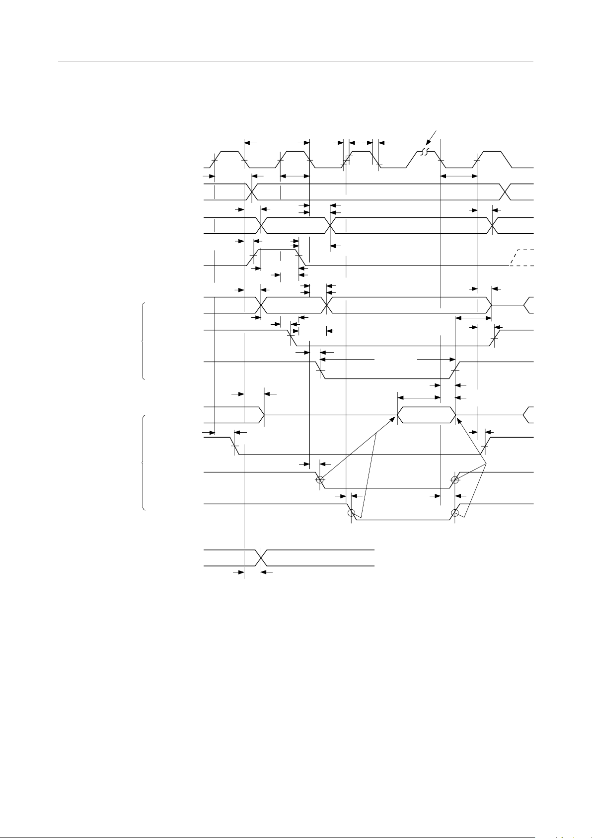
TIMING DIAGRAM
Input/Output A.C. Testing Load Circuit
2.4
1.5
Test Points
0.45
AC, Testing: Inputs are driven at 2.4 V
for a logic "1" and 0.45 V for a logic
"0". Timing measurements are 1.5 V for
both a logic "1" and "0".
Minimum Mode
CLK (MSM82C84A-2 Output)
BHE/S
, A19/S6 - A16/S
7
RDY (MSM82C84A-2 Input)
See NOTE 5
M/IO
3
ALE
Device
1.5
Under
Test
CL = 100 pF
C
includes jig capacitance.
L
t
CHDX
T
4
t
CLCH
T
1
t
CLCL
V
IH
V
IL
t
CHCTV
t
CLAV
t
CLLH
t
CHLL
t
CLAX
BHE, A
t
LHLL
t
AVAL
19
- A
T
2
t
CH1CH2tCL2CL1
t
CHCL
t
CLDV
16
t
LLAX
V
IH
V
IL
t
RYLCL
t
R1VCL
T
3
S7 - S
t
CLR1X
Tw
3
(MSM80C86A-10 Input)
Read Cycle
(NOTE 1)
(WR, INTA = V
OH
READY
)
AD
15
- AD
RD
DT/R
DEN
t
CHRYX
t
AVAL
t
LLAX
t
CLAV
AD
t
AZRL
15
- AD
0
t
CHCTV
0
t
CLRL
t
CVCTV
t
RYHCH
t
CLAZ
t
CLAX
Float
t
RLRH
t
DVCL
t
CLRH
t
CVCTX
Data In
t
CLDX
Float
t
RHAV
t
CHCTV
10/37
¡ Semiconductor MSM80C86A-10RS/GS/JS
Minimum Mode (continued)
CLK (MSM82C84A-2 Output)
BHE/S
, A19/S6 - A16/S
7
Write Cycle
AD
(NOTE 1)
(RD, INTA
DT/R = V
OH
)
INTA Cycle
AD
(NOTES 1&3)
OL
OH
)
(RD, WR = V
BHE = V
15
15
V
V
M/IO
ALE
- AD
DEN
WR
- AD
DT/R
INTA
T
1
t
CLCL
IH
IL
t
CHCTV
t
CLAV
3
t
CLLH
t
CLAV
0
0
BHE, A19 - A
t
t
t
CHLL
t
CVCTV
t
CHCTV
LHLL
AVAL
AD15 - AD
t
CVCTV
t
CLAZ
t
CVCTV
t
LLAX
t
0
t
CVCTV
t
CH1CH2
t
CHCL
16
AVAL
Float
T
t
t
t
t
CLDV
t
CLAX
2
CLDV
CLAX
LLAX
Data Out
t
WLWH
t
DVCL
T
3
t
CL2CL1
S7 - S
t
CVCTX
t
CVCTX
3
t
Pointer
T
W
WIDX
t
CHDX
t
CHDX
T
t
CLDX
4
t
CLCH
Float
t
CHCTV
t
CVCTX
Software Halt
RD, WR, INTA = V
OH
DT/R = Indeterminate
DEN
AD15 - AD
t
0
CLAV
Invalid Address
Software Halt
11/37
¡ Semiconductor MSM80C86A-10RS/GS/JS
Maximum Mode
CLK (MSM82C84A-2 Output)
QS0, QS
S2, S1, S0 (Except Halt)
BHE/S7, A19/S6 - A16/S
ALE
See
NOTE 5
(MSM82C88-2 Output)
RDY
(MSM82C84A-2 Input)
READY
(MSM80C86A-10 Input)
Read Cycle
AD
15
V
- AD
RD
DT/R
T
1
t
t
CLAX
t
CLAZ
A
15
CH1CH2
- A
19
- AD
t
AZRL
t
CLCL
IH
V
t
IL
CLAV
1
t
CHSV
t
CLAV
3
t
SVLH
t
CLLH
t
CLAV
0
t
CHDTL
BHE
AD
t
CHCL
16
t
CHLL
V
V
0
t
CLRL
IH
IL
T
t
CLDV
t
RYLCL
t
RYHSH
t
Float
2
t
CLAX
RYHCH
t
CL2CL1
t
R1VCL
t
RLRH
T
3
t
CLSH
S7 - S
t
CLR1X
t
DVCL
Data In
T
w
(See NOTE 8)
t
CHDX
3
t
t
CLRH
t
CLCH
t
CHRYX
CLDX
T
4
Float
t
RHAV
t
CHDTH
MSM82C88-2
Outputs
(See NOTES 5, 6)
MRDC or
IORC
DEN
t
CLML
t
CVNV
t
CLMH
t
CVNX
12/37

¡ Semiconductor MSM80C86A-10RS/GS/JS
Maximum Mode (continued)
CLK (MSM82C84A-2 Output)
S
, S1, S0 (Except Halt)
2
Write Cycle
MSM82C88-2 Outputs
See NOTES 5, 6
INTA Cycle
See NOTE 3, 4
MSM82C88-2 Outputs
See NOTES 5, 6
Software Halt
(DEN = V
; RD, MRDC, IORC, MWTC,
OL
AMWC, IOWC, AIOWC, INTA = V
V
V
AD15 - AD
DEN
AMWC or AIOWC
MWTC or IOWC
AD15 - AD
0
MCE/
PDEN
DT/R
INTA
DEN
)
OH
- AD
AD
15
S2, S1, S
T
1
IH
IL
t
CLAV
0
Float
t
SVMCH
t
CLMCH
0
t
CLAV
0
t
CHSV
t
CVNV
t
CVNX
t
CLML
t
CLAX
t
CLAZ
Invalid Address
Float
t
CHDTL
T
t
t
CLML
2
CLDV
Float
t
CVNV
T
t
CLSH
Data
t
CLMH
t
CLML
t
DVCL
Pointer
t
CVNX
(See
NOTE 8)
t
CHDX
t
CVNX
T
t
CLMH
4
t
CLDX
t
CLMH
Float
t
CHDTH
3
T
w
Notes: 1. All signals switch between VOH and VOL unless otherwise specified.
2. RDY is sampled near the end of T2, T3, TW to determine if TW machines
states are to be inserted.
3. Cascade address is valid between first and second INTA cycle.
4. Two INTA cycles run back-to-back. The MSM80C86A-10 LOCAL ADDR/
DATA BUS is floating during both INTA cycles. Control for pointer address
is shown for second INTA cycle.
5. Signals at MSM82C84A-2 or MSM82C88-2 are shown for reference only.
6. The issuance of the MSM 82C88-2 command and control signals (MRDC,
MWTC, AMWC, IORC, IOWC, AIOWC, INTA and DEN) lags the active
high MSM82C88-2 CEN.
7. All timing measurements are made at 1.5 V unless otherwise noted.
8. Status inactive in state just prior to T4
13/37

¡ Semiconductor MSM80C86A-10RS/GS/JS
≥ 50msec
t
DVCL
CLK
t
CLDX
Reset
V
CC
≥ 4 CLK Cycles
Asynchronous Signal Recognition
CLK
t
(See NOTE 1)
NMI
INTR
Signal
INVCH
TEST
NOTE: 1 Setup requirements for asynchronous
signals only to guarantee recognition
at next CLK
Bus Lock Signal Timing (Maximum Mode Only) Reset Timing
Any CLK Cycle Any CLK Cycle
CLK
t
CLAV
t
CLAV
LOCK
Request/Grant Sequence Timing (Maximum Mode Only)
Any CLK Cycle
> 0 CLK Cycle
CLK
RQ/GT
- AD
AD
15
0
A19/S6 - A16/S
S2, S1, S0,
t
CLGH
3
≥ t
CLCL
Coprocessor
MSM80C86A-10
t
t
Pulse 1
RQ
GVCH
CHGX
t
CLGL
Pulse 2
80C86AGT
≥ t
t
CLAZ
CLCL
t
CLGH
RD, CLOCK
BHE/S
7
NOTE: 1 The coprocessor may not drive the buses outside the region shown without risking contention.
Hold/Hold Acknowledge Timing (Minimum Mode Only)
Pulse 3
Coprocessor
Release
Coprocessor
(See NOTE 1)
MSM80C86A-10
≥ 1 CLK Cycle 1 or 2 Cycles
CLK
t
HVCH
t
HVCH
HOLD
t
CLHAV
t
CLHAV
HLDA
t
- AD0,
AD
15
- A16/S3,
A
19/S6
RD,
, M/IO
BHE/S
7
DT/R, WR, DEN
MSM80C86A-10
CLAZ
Coprocessor
MSM80C86A-10
14/37

¡ Semiconductor MSM80C86A-10RS/GS/JS
PIN DESCRIPTION
AD0 - AD
15
ADDRESS DATA BUS: Input/Output
These lines are the multiplexed address and data bus.
These are the address bus at the T1 cycle and the data bus at the T2, T3, TW and T4 cycles.
At the T1 cycle, AD0 low indicates Data Bus Low (D0-D7) Enable. These lines are high
impedance during interrupt acknowledge and hold acknowledge.
A16/S3. A17/S4, A18/S5, A19/S
6
ADDRESS/STATUS: Output
These are the four most significant addresses, at the T1 cycle. Accessing I/O port address,
these are low at T1 cycles. These lines are Status lines at T2, T3, TW and T4 cycles. S3 and S
are encoded as shown.
S
3
0
1
0
1
S
4
0
0
1
1
Characteristics
Alternate Data
Stack
Code or None
Data
These lines are high impedance during hold acknowledge.
4
BHE/S
7
BUS HIGH ENABLE/STATUS: Output
This line indicates Data Bus High Enable (BHE) at the T1 cycle. This line is status line at T2,
T3, TW and T4 cycles.
RD
READ: Output
This line indicates that CPU is in the memory or I/O read cycle.
This line is the read strobe signal when CPU read data from memory or I/O device. This line
is active low.
This line is high impedance during hold acknowledge.
READY
READY:Input
This line indicates to the CPU that the addressed memory or I/O device is ready to read or
write.
This line is active high. If the setup and hold time is out of specification, illegal operation will
occur.
INTR
INTERRUPT REQUEST: Input
This line is the level triggered interrupt request signal which is sampled during the last clock
cycle of instruction and string manipulation.
It can be internally masked by software.
This signal is active high and internally synchronized.
15/37

¡ Semiconductor MSM80C86A-10RS/GS/JS
INTA
INTERRUPT ACKNOWLEDGE: Output
This line is a read strobe signal for the interrupt acknowledge cycle. This line is active low.
TEST
TEST: Input
This line is examined by the WAIT instruction.
When TEST is high, the CPU enters idle cycle.
When TEST is low, the CPU exits the idle cycle.
NMI
NON MASKABLE INTERRUPT: Input
This line causes a type 2 interrupt.
NMI is not maskable.
This signal is internally synchronized and needs 2-clock cycles of pulse width.
RESET
RESET:Input
This signal causes the CPU to initialize immediately.
This signal is active high and must be at least four clock cycles.
CLK
CLOCK: Input
This signal provides the basic timing for the internal circuit.
MN/MX
MINIMUM/MAXIMUM: Input
This signal selects the CPU’s operating mode.
When VCC is connected, the CPU operates in Minimum mode.
When GND is connected, the CPU operates in Maximum mode.
V
CC
VCC: +5V supplied.
GND
GROUND
The following pin function descriptions are maximum mode only. Other pin functions are
already described.
SO, S1, S
2
STATUS: Output
These lines indicate bus status and they are used by the MSM82C88-2 Bus Controller to
generate all memory and I/O access control signals.
These lines are high impedance during hold acknowledge. These status lines are encoded as
shown.
16/37

¡ Semiconductor MSM80C86A-10RS/GS/JS
S
1
0
0
1
1
0
0
1
1
S
0
0
1
0
1
0
1
0
1
Characteristics
Interrupt acknowledge
Read I/O Port
Write I/O Port
Halt
Code Access
Read Memory
Write Memory
Passive
0 (LOW)
1 (HIGH)
RQ/GT
RQ/GT
S
2
0
0
0
1
1
1
0
1
REQUEST/GRANT:Input/Output
These lines are used for Bus Request from other devices and Bus GRANT to other devices.
These lines are bidirectional and active low.
LOCK
LOCK:Output
This line is active low.
When this line is low, other devices cannot gain control of the bus.
This line is high impedance during hold acknowledge.
QS0/QS
1
QUEUE STATUS: Output
These lines are Queue Status, and indicate internal instruction queue status.
QS1
0 (LOW)
0
1 (HIGH)
1
QS0
0
1
0
1
Characteristics
No operation
First Byte of Op Code from Queue
Empty the Queue
Subsequent Byte from Queue
The following pin function descriptions are minimum mode only. Other pin functions are
already described.
M/IO
STATUS: Output
This line selects memory address space or I/O address space.
When this line is high, the CPU selects memory address space and when it is low, the CPU
selects I/O address space.
This line is high impedance during hold acknowledge.
WR
WRITE: Output
This line indicates that the CPU is in the memory or I/O write cycle.
This line is a write strobe signal when the CPU writes data to memory of I/O device.
This line is active low.
This line is high impedance during hold acknowledge.
17/37

¡ Semiconductor MSM80C86A-10RS/GS/JS
INTA
INTERRUPT ACKNOWLEDGE: Output
This line is a read strobe signal for the interrupt acknowledge cycle. This line is active low.
ALE
ADDRESS LATCH ENABLE: Output
This line is used for latching the address into the MSM82C12 address latch. It is a positive
pulse and its trailing edge is used to strobe the address. This line is never floated.
DT/R
DATA TRANSMIT/RECEIVE: Output
This line is used to control the output enable of the bus transceiver.
When this line is high, the CPU transmits data, and when it is low. the CPU receives data.
This line is high impedance during hold acknowledge.
DEN
DATA ENABLE: Output
This line is used to control the output enable of the bus transceiver.
This line is active low. This line is high impedance during hold acknowledge.
HOLD
HOLD REQUEST: Input
This line is used for Bus Request from other devices.
This line is active high.
HLDA
HOLD ACKNOWLEDGE: Output
This line is used for Bus Grant other devices.
This line is active high.
18/37

¡ Semiconductor MSM80C86A-10RS/GS/JS
FUNCTIONAL DESCRIPTION STATIC OPERATION
The MSM80C86A-10 circuitry is of static design. Internal registers, counters and latches are
static and require no refresh as with dynamic circuit design. This eliminates the minimum
operating frequency restriction placed on other microprocessors. The MSM80C86A-10 can
operate from DC to the appropriate upper frequency limit. The processor clock may be stopped
in either state (high/low) and held there indefinitely. This type of operation is especially useful
for system debug or power critical applications.
The MSM80C86A-10 can be single stepped using only the CPU clock. This state can be
maintained as long as is necessary. Single step clock operation allows simple interface circuitry
to provide critical information for bringing up your system.
Static design also allows very low frequency operation (down to DC). In a power critical
situation, this can provide extremely low power operation since MSM80C86A-10 power
dissipation is directly related to operating frequency. As the system frequency is reduced, so
is the operating power until, ultimately, at a DC input frequency, MSM80C86A-10 power
requirement is the standby current (500mA maximum).
General Operation
The internal function of the MSM80C86A-10 consists of a Bus Interface Unit (BIU) and an
Execution Unit (EU). These units operate mutually but perform as separate processors.
BIU performs instruction fetch and queueing, operand fetch, DATA read and write address
relocation and basic bus control. Instruction pre-fetch is performed while waiting for decording
and execution of instructions. Thus, the CPU’s performance is increased. Up to 6-bytes of
instructions stream can be queued.
The EU receives pre-fetched instructions from the BIU queue, decodes and executes the
instructions, and provides the un-relocated operand address to BIU.
Memory Organization
The MSM80C86A-10 has a 20-bit address to memory. Each address has an 8-bit data width.
Memory is organized 00000H to FFFFFH and is logically divided into four segments: code, data,
extra data and stack segment. Each segment contains up to 64 Kbytes and locates on a 16-byte
boundary. (Fig. 3a)
All memory references are made relative to the segment register which functions in accordance
with a select rule. Word operands can be located on even or odd address boundary.
The BIU automatically performs the proper number of memory accesses. Memory consists of
an even address and an odd address. Byte data of even address is transferred on the AD0-AD
and byte data of odd address is transfered on the AD8-AD15.
The CPU provides two enable signals BHE and A0 to access either an odd address, even address
or both:
Memory location FFFF0H is the start address after reset, and 00000H through 003FFH are
reserved as an interrupt pointer, where there are 256 types of interrupt pointers.
Each interrupt type has a 4-byte pointer element consisting of a 16-bit segment address and a
16-bit offset address.
7
19/37

¡ Semiconductor MSM80C86A-10RS/GS/JS
Memory Organization Reserved Memory Locations
Segment
Register File
CS
SS
DS
ES
64KB
+Offset
FFFFFH
Code Segment
XXXXOH
Stack Segment
Data Segment
Extra Data Segment
OOOOH
Reset Bootstrap
Program Jump
Interrupt Pointer
for Type 255
Interrupt Pointer
for Type 1
Interrupt Pointer
for Type 0
FFFFFH
FFFFOH
3FFH
3FCH
7H
4H
3H
0H
Memory Reference Need Segment Selection Rule
Instructions
Stack
Local Data
External (Global Data)
Segment Register Used
CODE (CS)
STACK (CS)
DATA (DS)
EXTRA (ES)
Automatic with all instruction prefetch.
All stack pushes and pops. Memory references
relative to BP base register except data references.
Data references when relative to stack, destination
of string operation, or explicitly overridden.
Destination of string operations: Explicitly
selected using a segment overriden.
20/37

¡ Semiconductor MSM80C86A-10RS/GS/JS
Minimum and Maximum Modes
The MSM80C86A-10 has two system modes: minimum and maximum. When using maximum
mode, it is easy to organize a multi-CPU system with a MSM82C88-2 Bus Controller which
generates the bus control signal.
When using minimum mode, it is easy to organize a simple system by generating bus control
signal by itself.
MN/MX is the mode select pin. Definition of 24-31 pin changes depend on the MN/MX pin.
Bus Operation
The MSM80C86A-10 has a time multiplexed address and data bus. If a non-multiplexed bus is
desired for a system, it is only to add the address latch.
A CPU bus cycle consists of at least four clock cycles: T1, T2, T3 and T4. (Fig. 4)
The address output occurs during T1 and data transfer occurs during T3 and T4. T2 is used for
changing the direction of the bus at the read operation. When the device which is accessed by
the CPU is not ready for The data transfer and the CPU “NOT READY”, TW cycles are inserted
between T3 and T4.
When a bus cycle is not needed, T1 cycles are inserted between the bus cycles for internal
execution. During the T1 cycle, the ALE signal is output from the CPU or the MSM82C88-2
depending on MN/MX. At the trailing edge of ALE, a valid address may be latched.
Status bits S0, S1 and S2 are used in the maximum mode by the bus controller to recognize the
type of bus operation according to the following table.
Status bits S3 through S7 are multiplexed with A16 - A19, and BHE: therefore, they are valid
during T2 through T4.
S3 and S4 indicate which segment register was selected on the bus cycle, according to the
following table.
S
2
0 (LOW)
0
0
0
1 (HIGH)
1
1
1
S
1
0
0
1
1
0
0
1
1
S
0
0
1
0
1
0
1
0
1
Characteristics
Interrupt acknowledge
Read I/O
Write I/O
Halt
Instruciton Fetch
Read Data from Memory
Write Data to Memory
Passive (no bus cycle)
S
4
0 (LOW)
0
1 (HIGH)
1
S5 indicates interrupt enable Flag.
S
3
0
1
0
1
Characteristics
Alternate Data (Extra segment)
Stack
Code or None
Data
I/O Addressing
The MSM80C86A-10 has 64 Kbytes of I/O or as 32 Kwords I/O. When the CPU accesses an I/
O device, addresses AD0 - AD15 are in the same format as a memory address, and A16 - A19 are
low.
The I/O ports addresses are same as memory, so it is necessary to be careful when using 8-bit
peripherals.
21/37

¡ Semiconductor MSM80C86A-10RS/GS/JS
Basic System Timing
CLK
ALE
, S1, S
S
2
ADDR/
STATUS
ADDR/DATA
(4 + N*WAIT) = T
T
T
1
T3T
2
CY
TWAIT
T
4
(4 + N*WAIT) = T
T
T
1
2
T3T
CY
TWAIT
T
4
GOES INACTIVE IN THE STATE
JUST PRIOR TO T
0
BHE, A19 - A
A15 - A
0
16
S7 - S
3
BUS RESERVED
FOR DATA IN
A
- A
15
BHE, A19 - A
D15 - D
0
VALID
Data Out (D15 - D0)
0
4
16
S7 - S
3
RD, INTA
READY
DT/R
DEN
WR
READYREADY
WAITWAIT
MEMORY ACCESS TIME
22/37

¡ Semiconductor MSM80C86A-10RS/GS/JS
EXTERNAL INTERFACE
Reset
CPU Initialization is executed by the RESET pin. The MSM80C86A-10’s RESET High signal is
required for greater than 4 clock cycles.
The Rising edge of RESET terminates present operation immediately. The Falling edge of
RESET triggers an internal reset sequence for approximately 10 clock cycles. After the internal
reset sequence is finished normal operation occurs from absolute location FFFF0H.
Interrupt Operations
Interrupt operation is classified as software or hardware, and hardware interrupt is classified
as non-maskable or maskable.
An interrupt causes a new program location defined on the interrupt pointer table, according
to the interrupt type. Absolute locations 00000H through 003FFH are reserved for the interrupt
pointer table. The interrupt pointer table consists of 256-elements. Each element is 4 bytes in
size and corresponds to an 8-bit type number which is sent from an interrupt request device
during the interrupt acknowledge cycle.
Non-maskable Interrupt (NMI)
The MSM80C86A-10 has a Non-maskable interrupt (NMI) which is of higher priority than the
markable interrupt request (INTR).
The NMI request pulse width needs a minimum of 2 clock cycles. The NMI will be serviced at
the end of the current instruction or between string manipulations.
Maskable Interrupt (INTR)
The MSM80C86A-10 provides another interrupt request (INTR) which can be masked by
software. INTR is level triggered, so it must be held until the interrupt request is acknowledged.
INTR will be serviced at the end of the current instruction or between string manipulations.
Interrupt Acknowledge Sequence
T
ALE
T
1
T
2
3
T
4
TIT
T
1
T
2
T
3
4
AD
0
LOCK
INTA
AD
-
15
Float
Type Vector
23/37

¡ Semiconductor MSM80C86A-10RS/GS/JS
Interrupt Acknowledge
During the interrupt acknowledge sequence, further interrupts are disabled. The interrupt
enable bit is reset by any interrupt, after which the Flag register is automatically pushed onto
the stack. During the acknowledge sequence, the CPU emits the lock signal from T2 of the first
bus cycle to T2 of the second bus cycle. At second bus cycles, byte is fetched from the external
device as a vector which identified the type of interrupt. This vector is multiplied by four and
used as a interrupt pointer address. (INTR only)
The interrupt Return (IRET) instruction includes a Flag pop operation which returns the
original interrupt enable bit when it restores the Flag.
HALT
When a Halt instruction is executed, the CPU enters the Halt state. An interrupt request or
RESET will force the MSM80C86A-10 out of the Halt state.
System Timing – Minimum Mode
A bus cycle begins T1 with an ALE signal. The trailing edge of ALE is used to latch the address.
From T1 to T4 the M/IO signal indicates a memory or I/O operation. From T2 to T4, the address
data bus changes the address but to data bus.
The read (RD), write (WR) and interrupt acknowledge (INTA) signals causes the addressed
device to enable data bus. These signal becomes active at the beginning of T2 and inactive at
the beginning of T4.
System Timing – Maximum Mode
At maximum mode, the MSM82C88-2 Bus Controller is added to system. The CPU sends status
information to the Bus Controller. Bus timing signals are generated by Bus Controller. Bus
timing is almost the same as in the minimum mode.
24/37

¡ Semiconductor MSM80C86A-10RS/GS/JS
g
g
BUS HOLD CIRCUITRY
To avoid high current conditions caused by floating inputs to CMOS devices and to eliminate
the need for pull-up/down resistors, “bus-hold” circuitry has been used on MSM80C86A-10
pins 2-16, 26-32, and 34-39 (Figures 6a, 6b). These circuits will maintain the last valid logic state
if no driving source is present (i.e. an unconnected pin or a driving source which goes to a high
impedance state). To overdrive the “bus hold” circuits, an external driver must be capable of
supplying approximately 600 mA minimum sink or source current at valid input voltage levels.
Since this “bus hold” circuitry is active and not a “resistive” type element, the associated power
supply current is negligible and power dissipation is significantly reduced when compared to
the use of passive pull-up resistors.
"PULL-UP/PULL-DOWN"
OUTPUT
DRIVER
INPUT
BUFFER
INPUT
PROTECTION
CIRCUITRY
Input Buffer exists only on I/O pins
Fi
ure 6a. Bus Hold Circuitry Pin 2-16, 35-39
"PULL-UP"
OUTPUT
DRIVER
BOND
PAD
BOND
PAD
EXTERNAL
PIN
EXTERNAL
PIN
V
CC
INPUT
BUFFER
P
INPUT
PROTECTION
CIRCUITRY
Input Buffer exists only on I/O pins
ure 6b. Bus Hold Circuitry Pin 26-32, 34
Fi
25/37

¡ Semiconductor MSM80C86A-10RS/GS/JS
3210
data if w = 1
3210 7654
data
addr-high
addr-high
data if w = 1
0 7654
r/m
r/m
21
3
0
4
0
reg
data
addr-low
reg
addr-low
w
w
011
001
0
65
7
mod
mod
0
w
w
1d1
201
310w001
4001000
5001110
6010000
7111111
r/m
r/m
reg
reg
0
0
mod
mod
0
0
0
1
1
0
0
0
1
110 r/m
mod
1
1
reg
1
1
0
1
1
100
110
100
0
1
1
reg
000 r/m
mod
1
1
reg
1
1
1
0
1
000
010
100
1
1
1
reg
reg r/m
w mod
reg
11
0
0
0
1
0
0
0
0
1
1
port
w
w
0
0
1
1
0
1
0
0
1
1
1
1
1
1
r/m
r/m
r/m
reg
reg
mod
mod
reg
mod
port
1110100
w
w
111000110
111111111
010100111
001000111
110000000
111011000
111111111
1
0
1
1
1
0
0
1
MOV = Move:
Register/memory to/from register
Immediate to register/memory
Immediatye to register
Memory to accumulator
DATA TRANSFER
Accumulator to memory
Register/memory to segment register
Segment register to register/memory
PUSH = Push:
Register/memory
Register
Segment register
POP = Pop:
Register/memory
Register
Segment register
XCHG = Exchange:
Register/memory with register
Register with accumulator
IN = Input from:
Fixed port
Variable port
OUT = Output to:
Fixed port
Variable port
XLAT = Translate byte to AL
LEA = Load EA to register
LDS = Load pointer to DS
LES = Load pointer to ES
LAHF = Load AH with flags
SAHF = Store AH into flags
PUSHF = Push flags
POPF = Pop flags
26/37

¡ Semiconductor MSM80C86A-10RS/GS/JS
data if s:w = 01
data
data if w = 1
r/m
r/m
0
reg
mod
mod 0 0
www
ds0
001
000
000
000
000
010
r/m
reg
data
mod
www
ds0
001
000
101
000
000
010
mod 0 0 0 r/m
w
1
reg
1
100
101
101
110
100
1
1
1
data if s:w = 01
data if w = 1
r/m data
0
data
mod 0 1
r/m
r/m
1
0
0
mod
w
1
reg
1
110
101
101
111
101
1
1
0
mod
w
1
1
data if s:w = 01
data if w = 1
r/m
r/m data
1
reg
data
mod
mod 1 1
www
ds0
001
101
101
101
000
010
1
1
1
1
1
1
0
0
data if s:w = 01
data if w = 1
r/m
r/m data
1
reg
data
mod
mod 1 0
1
www
1
ds0
1
001
0
101
0
000
1
101
0
000
0
010
data if s:w = 01
data if w = 1
r/m
r/m data
1
reg
data
mod
mod 0 1
www
ds0
001
101
101
000
000
010
ADD = Add:
Reg./memory with register to either
Immediate to register/memory
ARITHMETIC
Immediate to accumulator
ADC = Add with carry:
Reg./memory with register to either
Immediate to register/memory
Immediate to accumulator
INC = Increment:
Register/memory
Register
AAA = ASCII adjust for add
DAA = Decimal adjust for add
SUB = Subtract:
Reg./memory with register to either
Immediate from register/memory
Immediate from accumulator
SBB = Subtract with borrow:
Reg./memory with register to either
Immediate from register/memory
Immediate from accumulator
DEC = Decrement:
Register/memory
Register
NEG = Change sign
CMP = Compare:
Register/memory and register
Immediate with register/memory
Immediate with accumulator
AAS = ASCII adjust for subtract
27/37

¡ Semiconductor MSM80C86A-10RS/GS/JS
0
r/m
r/m1r/m
0
01101
00011
11011
0
mod
mod0 mod
1
w
w0w
111011000
111111100
100000011
011111111
111011000
011111100
011111111
0
1
r/m
0
1
0
0
0
0
mod
101
w
DAS = Decimal adjust for subtract
MUL = Multiply (unsigned)
IMUL = Integer multiply (signed)
AAM = ASCII adjust for multiply
DIV = Divide (unsigned)
IDIV = Integer divide (signed)
AAD = ASCII adjust for divide
CBW = Convert byte to word
CWD = Convert word to double word
28/37

¡ Semiconductor MSM80C86A-10RS/GS/JS
r/m
r/m
r/m
r/m
r/m
r/m
0011010
1001001
0111000
mod
mod
mod
mod
mod
mod
wwwwwww
vvvvvvv
1
1000000
0000000
1111111
1000000
1111111
1111111
r/m
r/m
1
1
0
mod
mod
w
0
0
1
0
1
1
data if w = 1
data if w = 1
r/m
r/m data
0
reg
data
mod
mod 1 0
www
d00
001
000
000
101
000
010
data if w = 1
data if w = 1
r/m
r/m data
0
reg
data
mod
mod 0 0
www
010
110
001
010
011
010
111
data if w = 1
data if w = 1
r/m
r/m data
1
reg
data
mod
mod 0 0
www
d00
001
101
000
000
000
010
data if w = 1
data if w = 1
r/m
r/m data
0
reg
data
mod
mod 1 1
www
d00
001
000
101
101
000
010
NOT = Invert
LOGIC
SHL/SAL = Shift logical/arithmetic left
SHR = Shift logical right
SAR = Shift arithmetic right
ROL = Rotate left
ROR = Rotate right
RCL = Rotate left through carry
RCR = Rotate right through carry
AND = And:
Reg./memory and register to either
Immediate to register/memory
Immediate to accumulator
TEST = And function to flags, no result:
Register/memory and register
Immediate data and register/memory
Immediate data and accumulator
OR = Or:
Reg./memory and register to either
Immediate to register/memory
Immediate to accumulator
XOR = Exclusive or:
Reg./memory and register to either
Immediate to register/memory
Immediate to accumulator
29/37

¡ Semiconductor MSM80C86A-10RS/GS/JS
z
wwwww
10110
01111
00011
10000
11111
10000
11111
disp
disp
disp
disp
disp
disp
disp
disp
disp
disp
disp
disp
disp
0000000011111111010
1
0011110000111100100
0
1110100011101000000
1
0110010101100101000
0
1111111111111111100
1
1111111111111111111
0
1111111111111111111
1
0000000000000000111
disp
disp
disp
disp
disp
disp
disp
1
1
0
0
0
1
1
1
type
100
001
111
111
000
000
111
111
1
1
1
1
0
0
1
1
REP = Repeat
MOVS = Move byte/word
CMPS = Compare byte/word
SCAS = Scan byte/word
LODS = Load byte/word to AL/AX
STOS = Store byte/word from AL/AX
CJMP = Conditional JMP
STRING MANIPULATION
JE/JZ = Jump on equal/zero
JZ/JNGE = Jump on less/not greater or equal
JLE/JNG = Jump on less or equal/not greater
JB/JNAE = Jump on below/not above or equal
JBE/JNA = Jump on below or equal/not above
JP/JPE = Jump on parity/parity even
JO = Jump on over flow
JS = Jump on sign
JNE/JNZ = Jump on not equal/not zero
JNL/JGE = Jump on not less/greater or equal
JNLE/JG = Jump on not less or equal/greater
JNB/JAE = Jump on not below/above or equal
JNBE/JA = Jump on not below or equal/above
JNP/JPO = Jump on not parity/parity odd
JNO = Jump on not overflow
JNS = Jump on not sign
LOOP = Loop CX times
LOOPZ/LOOPE = Loop while zero/equal
LOOPNZ/LOOPNE = Loop while not zero equal
JCXZ = Jump on CX zero
INT = Interrupt
Type specified
Type 3
INTO = Interrupt on overflow
IRET = Interrupt return
30/37

31/37
¡ Semiconductor MSM80C86A-10RS/GS/JS
CLC = Clear carry
CMC = Complementary carry
STC = Set carry
CLD = Clear direction
STD = Set direction
CLI = Clear interrupt
STI = Set interrupt
HLT = Halt
WAIT = Wait
ESC = Escape ( to external device)
LOCK = Bus lock prefix
1
1
1
1
1
1
1
1
1
1
1
1
1
1
1
1
1
1
1
0
1
1
1
1
1
1
1
1
1
1
0
0
1
1
1
1
1
1
1
1
1
1
1
1
1
0
1
1
1
1
1
0
1
1
0
0
1
0
1
1
0
0
1
0
x
0
0
0
0
0
0
1
1
0
1
x
0
0
1
1
0
1
0
1
0
1
x0 mod x x x r/m
PROCESSOR CONTROL
CALL = Call:
Direct within segment
Indirect within segment
Direct intersegment
Indirect intersegment
7
1
1
1
1
6
1
1
0
1
5
1
1
0
1
4
0
1
1
1
3
1
1
1
1
2
0
1
0
1
1
0
1
1
1
0
0
1
0
1
7
mod
mod
65
0
0
4
disp-low
1
offset-low
seg-low
1
3
0
1
21
r/m
r/m
0 7654
disp-high
offset-high
seg-high
3210 765 43210
JMP = Unconditional Jump:
Direct within segment
Direct within segment-short
Indirect within segment
Direct intersegment
Indirect intersegment
1
1
1
1
1
1
1
1
1
1
1
1
1
1
1
0
0
1
0
1
1
1
1
1
1
0
0
1
0
1
0
1
1
1
1
1
1
1
0
1
mod
mod
1
1
disp-low
disp
0
offset-low
seg-low
001
r/m
r/m
disp-high
offset-high
seg-high
RET = Return from CALL:
Within segment
Within seg. adding immediate to SP
Intersegment
Intersegment adding immediate to SP
1
1
1
1
1
1
1
1
0
0
0
0
0
0
0
0
0
0
1
1
0
0
0
0
1
1
1
1
1
0
1
0
data-low
data-low
data-high
dat-high
CONTROL TRANSFER

¡ Semiconductor MSM80C86A-10RS/GS/JS
Foot Notes: AL = 8-bit accumulator
AX = 18-bit accumulator
CX = Count register
DS = Data segment
ES = Extra segment
Above/below refers to unsigned value
Greater=more positive
Less=less positive (more negative) signed value
If d=1 then “to” reg: If d=0 then “from” reg.
If w=1 then word instruction: If w=0 then byte instruction
If mod=11 then r/m is treated as a REG field
If mod=00 then DISP=0*, disp-low and disp-high are absent
If mod=01 then DISP=disp-low sign-extended to 16 bits, disp-high is absent
If mod=10 then DISP=disp-high: disp-low
If r/m=000 then EA=(BX)+(SI)+DISP
If r/m=001 then EA=(BX)+(DI)+DISP
If r/m=010 then EA=(BP)+(SI)+DISP
If r/m=011 then EA=(BP)+(DI)+DISP
If r/m=100 then EA=(SI)+DISP
If r/m=101 then EA=(DI)+DISP
If r/m=110 then EA=(BP)+DISP*
If r/m=111 then EA=(BX)+DISP
DISP follows 2nd byte of instruction (before data if required)
* except if mod=00 and r/m=110 then EA-disp-high: disp-low
If s:w=01 then 16 bits of immediate data form the operand
If s:w=11 then an immediate data byte is sign extended to form the 16-bit operand
If v=0 then “count”=1:if v=1 then “count” in (CL)
x=don’ t care
z is used for string primitives for comparison with ZF FLAG
SEGMENT OVERRIDE PREFIX
001 reg 110
REG is assigned according to the following table:
16-Bit (w=1) 8-Bit (w=0) Segment
000 AX 000 AL 00 ES
001 CX 001 CL 01 CS
010 DX 010 DL 10 SS
011 BX 011 BL 11 DS
100 SP 100 AH
101 BP 101 CH
110 SI 110 DH
111 DI 111 BH
Instructions which reference the flag register file as a 16-bit object use the symbol
FLAGS to represent the file:
FLAGS=x:x:x:x:(OF):(DF):(IF):(TF):(SF):(ZF):X:(AF):X:(PF):X:(CF)
32/37

¡ Semiconductor MSM80C86A-10RS/GS/JS
NOTICE ON REPLACING LOW-SPEED DEVICES WITH HIGH-SPEED DEVICES
The conventional low speed devices are replaced by high-speed devices as shown below.
When you want to replace your low speed devices with high-speed devices, read the replacement
notice given on the next pages.
High-speed device (New)
M80C85AH
M80C86A-10
M80C88A-10
M82C84A-2
M81C55-5
M82C37B-5
M82C51A-2
M82C53-2
M82C55A-2
Low-speed device (Old)
M80C85A/M80C85A-2
M80C86A/M80C86A-2
M80C88A/M80C88A-2
M82C84A/M82C84A-5
M81C55
M82C37A/M82C37A-5
M82C51A
M82C53-5
M82C55A-5
Remarks
8bit MPU
16bit MPU
8bit MPU
Clock generator
RAM.I/O, timer
DMA controller
USART
Timer
PPI
33/37

¡ Semiconductor MSM80C86A-10RS/GS/JS
Differences between MSM80C86A-10 and MSM80C86A-2, MSM80C86A
1) Manufacturing Process
All devices use a 1.5 m Si-CMOS process technology.
2) Design
Although circuit timings of these devices are a little different, these devices have the same chip size
and logics.
3) Electrical Characteristics
Oki's '96 Data Book for MICROCONTROLLER describes that the MSM80C86A-10 satisfies the
electrical characteristics of the MSM80C86A-2 and MSM80C86A.
4) Other notices
1) The noise characteristics of the high-speed MSM80C86A-10 (for 10 MHz) are a little different from
those of the MSM80C86A-2 and MSM80C86A. Therefore when devices are replaced for upgrading,
it is recommended to perform noise evaluation.
2) The characteristics of the MSM80C86A-10 basically satisfy those of the MSM80C86A-2 and
MSM80C86A but their timings are a little different. When critical timing is required in designing
it is recommended to evaluate operating margins at various temperatures and voltages.
34/37

¡ Semiconductor MSM80C86A-10RS/GS/JS
PACKAGE DIMENSIONS
(Unit : mm)
DIP40-P-600-2.54
Package material
Lead frame material
Pin treatment
Solder plate thickness
Package weight (g)
Epoxy resin
42 alloy
Solder plating
5 mm or more
6.10 TYP.
Notes for Mounting the Surface Mount Type Package
The SOP, QFP, TSOP, SOJ, QFJ (PLCC), SHP and BGA are surface mount type packages, which
are very susceptible to heat in reflow mounting and humidity absorbed in storage.
Therefore, before you perform reflow mounting, contact Oki’s responsible sales person for the
product name, package name, pin number, package code and desired mounting conditions
(reflow method, temperature and times).
35/37

¡ Semiconductor MSM80C86A-10RS/GS/JS
(Unit : mm)
QFJ44-P-S650-1.27
Mirror finish
Package material
Lead frame material
Pin treatment
Solder plate thickness
Package weight (g)
Epoxy resin
Cu alloy
Solder plating
5 mm or more
2.00 TYP.
Notes for Mounting the Surface Mount Type Package
The SOP, QFP, TSOP, SOJ, QFJ (PLCC), SHP and BGA are surface mount type packages, which
are very susceptible to heat in reflow mounting and humidity absorbed in storage.
Therefore, before you perform reflow mounting, contact Oki’s responsible sales person for the
product name, package name, pin number, package code and desired mounting conditions
(reflow method, temperature and times).
36/37

¡ Semiconductor MSM80C86A-10RS/GS/JS
(Unit : mm)
QFP56-P-1519-1.00-K
Mirror finish
Package material
Lead frame material
Pin treatment
Solder plate thickness
Package weight (g)
Epoxy resin
42 alloy
Solder plating
5 mm or more
1.46 TYP.
Notes for Mounting the Surface Mount Type Package
The SOP, QFP, TSOP, SOJ, QFJ (PLCC), SHP and BGA are surface mount type packages, which
are very susceptible to heat in reflow mounting and humidity absorbed in storage.
Therefore, before you perform reflow mounting, contact Oki’s responsible sales person for the
product name, package name, pin number, package code and desired mounting conditions
(reflow method, temperature and times).
37/37
 Loading...