

OKI MSM80C51F-xxxJS, MSM80C51F-xxxRS, MSM80C31F-xxxGS, MSM80C31F-xxxJS, MSM80C51F-xxxGS Datasheet
...
E2E1037-19-41
¡ Semiconductor MSM80C31F/80C51F
This version: Mar. 1995
¡ Semiconductor
MSM80C31F/MSM80C51F
CMOS 8-Bit Microcontroller
GENERAL DESCRIPTION
The OKI MSM80C31F/MSM80C51F microcontroller is a low-power, 8-bit device implemented
in OKI's silicon-gate complementary metal-oxide semiconductor process technology. The
device
data RAM, 32 I/O lines, two 16-bit timer/counters, a five-source two-level interrupt
structure, a full duplex
has two software selectable modes for further power reduction — Idle and Power Down. Idle
mode freezes the CPU's in-struction execution while maintaining RAM and allowing the timers,
serial port and interrupt system to continue functions. Power Down mode saves the RAM
contents but freezes the oscillator causing all other device functions to be inoperative.
includes 4K bytes of mask programmable ROM (MSM80C51F only), 128 bytes of
serial port, and an oscillator and clock circuitry. In addition, the device
FEATURES
• Low power consumption by 2 mm silicon gate CMOS process technology
• Fully static circuit
• Internal program memory : 4K bytes (MSM80C51F)
• External program memory space : 64K bytes
• Internal data memory (RAM) : 128 bytes
• External data memory (RAM) space : 64K bytes
• I/O ports : 8-bit ¥ 4 ports
• Two 16-bit timer/counters
• Multifunctional serial port (UART)
• Five interrupt sources (Priority can be set)
• Four sets of working registers (R0-7 ¥ 4)
• Stack : Internal data memory (RAM)
128-byte area can be used arbitrarily (by SP specified)
• Two CPU power-down modes
(1) Idle mode : CPU stopped while oscillation continued.
(Software setting)
(2) PD mode : CPU and oscillation all stopped.
(Software setting)
(Setting I/O ports to floating status possible)
• Operating temperature : –40 to +85°C (@ 12 MHz, V
–20 to +70°C (@ 16 MHz, V
• 2-byte 1-machine cycle instructions : 1 msec. @ 12 MHz
0.75 msec. @ 16 MHz
• Multiplication/division instructions : 4 msec. @ 12 MHz
3 msec. @ 16 MHz
• Instruction code addressing method
Byte specification : Data addressing (direct)
Bit specification : Bit addressing
= 5 V ±20%)
CC
= 5 V ±5%)
CC
1/38

¡ Semiconductor MSM80C31F/80C51F
• Package options
40-pin plastic DIP (DIP40-P-600-2.54) : (MSM80C31F-¥¥¥RS) (MSM80C51F-¥¥¥RS)
44-pin plastic QFP (QFP44-P-910-0.80-2K) : (MSM80C31F-¥¥¥GS) (MSM80C51F-¥¥¥GS)
44-pin plastic QFJ (PLCC) (QFJ44-P-S650-1.27) : (MSM80C31F-¥¥¥JS) (MSM80C51F-¥¥¥JS)
¥¥¥ indicates the code number.
DIFFERENCES BETWEEN MSM80C31F/MSM80C51F AND MSM80C31/MSM80C51
• Operating frequency
0.5 to 16 MHz ..................... MSM80C31F-1/MSM80C51F-1
0.5 to 12 MHz ..................... MSM80C31/MSM80C51/MSM80C31F/MSM80C51F
• External clock input terminal
XTAL1 ................................. MSM80C31F(-1)/MSM80C51F(-1)
XTAL2 ................................. MSM80C31/MSM80C51
• Emulation mode
Output impedance of ALE and PSEN pins becomes about 20 kW while CPU is being reset in
MSM80C31F/MSM80C51F.
Any other functions and electrical characteristics of MSM80C31F/MSM80C51F except for
above three differences are the same as those of MSM80C31/MSM80C51.
2/38
3/38
¡ Semiconductor MSM80C31F/80C51F
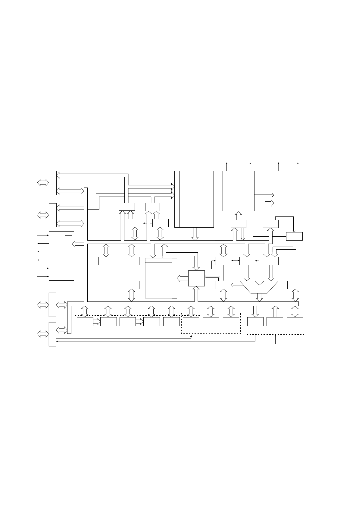
BLOCK DIAGRAM
PCH
CONTROL SIGNALS
SPECIAL
FUNCTION
REGISTER
ADDRESS
DECODER
PLA
IR AIR
C-ROM
TR1
TR2ACC
ALU
BR
PSW
RAMDP
R/W AMP
128 WORDS
¥ 8 BITS
DPLDPH
PCL
ROM
4096 WORDS
¥ 8 BITS
SENSE AMP
PCLL
PCHL
PORT 2 PORT 0
PCON
OSC AND TIMING
PORT 1 PORT 3
XTAL1
XTAL2
ALE
RESET
PSEN
EA
TH1 TL1 TH0 TL0 TMOD TCON IE IP SBUF(T) SBUF(R)
INTERRUPT
TIMER/COUNTER
SERIAL IO
SCON
SIGNALSR/W
SP
ADDRESS DECODER
ADDRESS DECODER
P2.0 to P2.7
P0.0 to P0.7
P1.0 to P1.7
P3.0 to P3.7
4/38
¡ Semiconductor MSM80C31F/80C51F
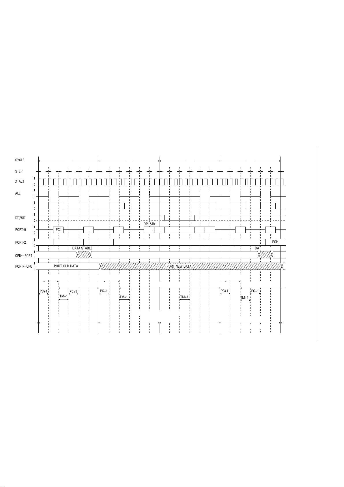
CLOCK WAVEFORMS
Basic Timing Chart
ACC & RAM
S1 S2 S3 S4 S5 S6M1S1 S2 S3 S4 S5 S6M1S1 S2 S3 S4 S5 S6M2S1 S2 S3 S4 S5 S6
M1
PCL PCL PCL PCL
PCH PCH PCH PCHPCHDPH & PORT DATAPCH
,,,,,,,,,,,
,,,,,,,,,,,,,,
,,,,,,,,,,,,,,,,,
,,,,,,,,,,,,,,,,,
,,,,,,,,,,,,,,,,,,
,,,,,,,,,,,,,,,,,,
,,,,,,,,,,,,,,,,,,
,,,,,,,,,,,,,,,,,,
,,,,,,,,,,,,
PORT NEW DATA
PC+1
TM+1
PC+1
TM+1
TM+1
TM+1
PC+1PC+1PC+1
CYCLE
STEP
1
0
1
0
1
0
1
0
1
0
1
0
1
0
1
0
XTAL1
ALE
RD/WR
PORT-0
PORT-2
CPU¨PORT
PORT¨CPU
PCH
PCL
DPL&Rr
DATA STABLE
PORT OLD DATA
DATA STABLE
PSEN
PCL
Instruction decoding
Instruction execution
Instruction decoding
Instruction execution
Instruction decoding
Instruction execution
Port output/input
Instruction execution
Port output/input
Instruction execution
execution
External data memory instruction
¡ Semiconductor MSM80C31F/80C51F
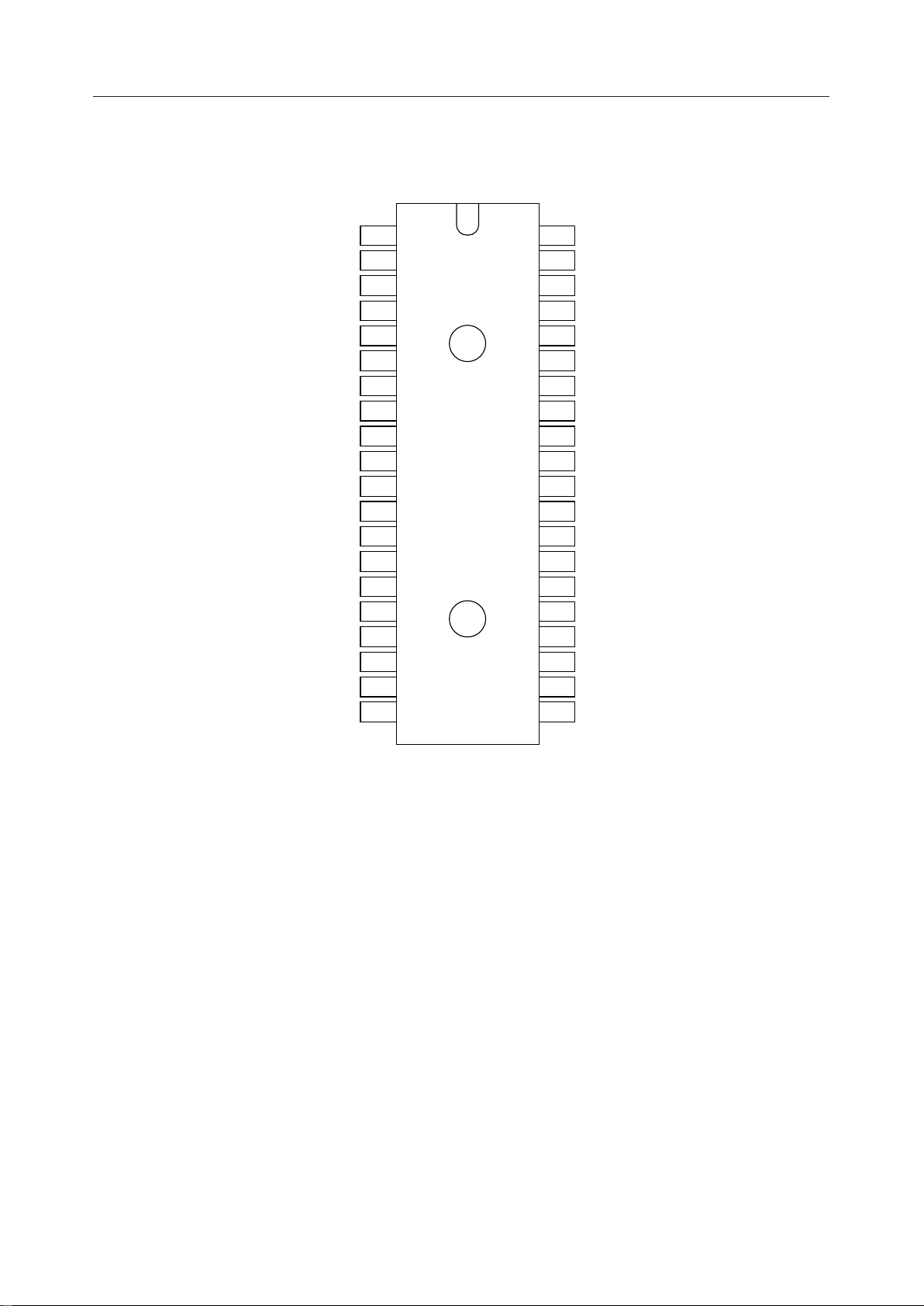
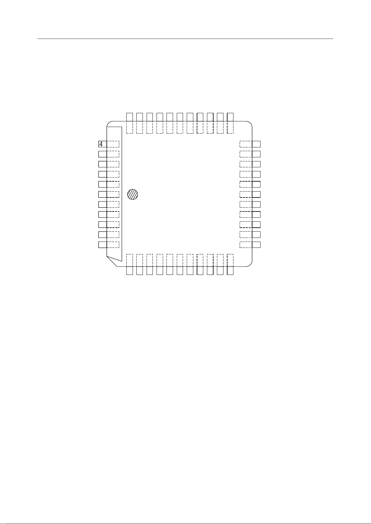
PIN CONFIGURATION (TOP VIEW)
P1.0
P1.1
P1.2
P1.3
P1.4
P1.5
P1.6
P1.7
RESET
RXD/P3.0
TXD/P3.1
INT0/P3.2
INT1/P3.3
T0/P3.4
T1/P3.5
WR/P3.6
RD/P3.7
XTAL2
XTAL1
V
SS
10
11
12
13
14
15
16
17
18
19
20
1
2
3
4
5
6
7
8
9
40
39
38
37
36
35
34
33
32
31
30
29
28
27
26
25
24
23
22
21
V
CC
P0.0
P0.1
P0.2
P0.3
P0.4
P0.5
P0.6
P0.7
EA
ALE
PSEN
P2.7
P2.6
P2.5
P2.4
P2.3
P2.2
P2.1
P2.0
40-Pin Plastic DIP
5/38
¡ Semiconductor MSM80C31F/80C51F
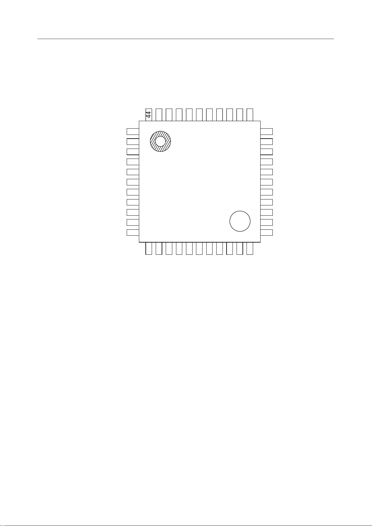
PIN CONFIGURATION (TOP VIEW) (continued)
P1.5
P1.6
P1.7
RESET
P3.0/RXD
NC
P3.1/TXD
P3.2/INT0
P3.3/INT1
P3.4/T0
P3.5/T1/HPDI
1
2
3
4
5
6
7
8
9
10
11
P1.4
44
12
P3.6/WR
P1.3
43
13
P3.7/RD
P1.2
P1.1
42
41
14
15
XTAL2
XTAL1
P1.0NCV
40
39
16
17
SSVSS
V
CC
38
18
P2.0
P0.0
37
19
P2.1
P0.1
36
20
P2.2
P0.2
35
21
P2.3
P0.3
34
22
P2.4
33
32
31
30
29
28
27
26
25
24
23
P0.4
P0.5
P0.6
P0.7
EA
NC
ALE
PSEN
P2.7
P2.6
P2.5
44-Pin Plastic QFP
6/38
¡ Semiconductor MSM80C31F/80C51F
)
PIN CONFIGURATION (TOP VIEW) (continued)
P0.5
P0.6
P0.4
39
38
P0.7EANC
37
36
35
34
ALE
33
PSEN
32
P2.7
31
P2.6
30
P2.5
29
P0.3
P0.2
P0.1
P0.0
V
CC
NC
P1.0
P1.1
P1.2
P1.3
P1.4
40
41
42
43
44
P2.4
28
27
P2.3
26
P2.2
25
P2.1
24
P2.0
1
2
3
4
5
6
7
8
9
10
11
12
13
14
15
16
17
P1.5
P1.6
P1.7
RESET
NC
P3.0/RXD
P3.1/TXD
P3.2/INT0
P3.3/INT1
P3.4/T0
P3.5/T1
23
22
21
20
19
18
NC
V
SS
XTAL1
XTAL2
P3.7/RD
P3.6/WR
44-Pin Plastic QFJ (PLCC
7/38

¡ Semiconductor MSM80C31F/80C51F
PIN DESCRIPTION
Symbol Description
V
SS
V
CC
Port 0.0
- 0.7
Port 1.0
- 1.7
Port 2.0
- 2.7
Port 3.0
- 3.7
RESET
ALE
PSEN
EA
XTAL1
XTAL2
Ground potential
Supply voltage during Normal, Idle and Power Down operation
Port 0 is an 8-bit open-drain bidirectional I/O port. It is also the mutiplexed low-order address
and data bus during accesses to external memory.
Port 1 is an 8-bit bidirectional I/O port with internal pull-ups. It can drive CMOS inputs without
external pull-ups.
Port 2 is an 8-bit bidirectional I/O port with internal pull-ups. It outputs the high-order address
byte during accesses to external memory. It can drive CMOS inputs without external pull-ups.
Port 3 is an 8-bit bidirectional I/O port with internal pull-ups. It also provides various special
features, as shown below:
Port Pin
P3.0
P3.1
P3.2
P3.3
P3.4
P3.5
P3.6
P3.7
Alternate Function
RXD
TXD
INT0
INT1
T0
T1
WR
RD
(serial input port)
(serial output port)
(external interrupt)
(external interrupt)
(Timer 0 external input)
(Timer 1 external input)
(external data memory write strobe)
(external data memory read strobe)
Port 3 can drive CMOS inputs without external pull-ups.
Reset input pin. A reset is accomplished by holding the RESET pin high for at least 1ms.
even if the oscillator has been stopped. The CPU responds by executing an internal reset. An
internal pull-down resistor permits Power-On reset using only a capacitor connected to V
CC
.
This pin does not receive the power down voltage since the function has been transferred to the
pin.
V
CC
Address Latch Enable. This output latches for latching the low byte of the address during
accesses to external memory. For this purpose, ALE is activated twice every machine cycle or
at a constant rate of 1/6th the oscillator frequency, except during an external memory access at
which time one ALE pulse is skipped. ALE can drive CMOS inputs without an external pull-up.
Program Store Enable output. This output is the read strobe to external program memory.
For this purpose, PSEN is activated twice every machine cycle. (However, when executing out
of external program memory, two activations of PSEN are skipped during each access to
external data memory.) PSEN is not activated during fetches from internal program memory.
It can drive CMOS inputs without an external pull-up.
External Access input pin. When EA is held high, the CPU executes out of internal program
memory (unless the program counter exceeds 0FFFH).
When EA is held low, the CPU executes only out of external program memory.
EA must not be floated.
Crystal 1 pin. It is an input to the inverting amplifier which forms the internal oscillator.
Crystal 2 pin. It is an output of the inverting amplifier that forms the internal oscillator.
8/38
¡ Semiconductor MSM80C31F/80C51F
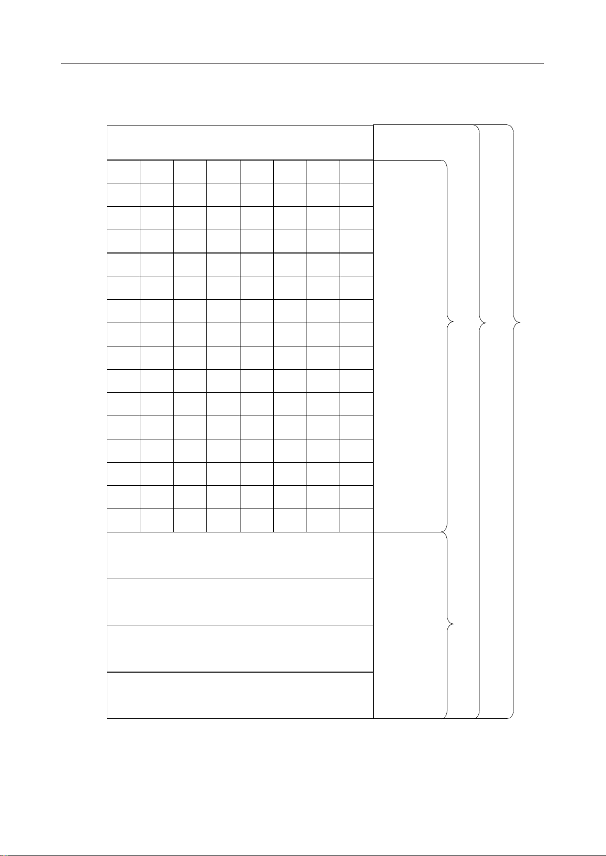
DATA MEMORY AND SPECIAL FUNCTION REGISTER LAYOUT DIAGRAM
7F
30
7F
2F
BIT
7
20
R7
1F
R0
18
DATA RAM
17
10
0F
08
07
00
R7
R0
R7
R0
R7
R0
USER RAM
80W ¥ 8 bits
ADDRESSABLE
RAM
BANK 3
BANK 2
BANK 1
BANK 0
78
0F0H
0E0H
0D0H
0B8H
0B0H
0A8H
0A0H
99H
98H
90H
8DH
8CH
8BH
8AH
89H
SPECIAL FUNCTION REGISTERS
0
88H
87H
83H
82H
81H
80H
BIT ADDRESSING
DATA ADDRESSING
B
ACC
PSW
IP
P3
IE
P2
SBUF
SCON
P1
TH1
TH0
TL1
TL0
TMOD
TCON
PCON
DPH
DPL
SP
P0
9/38
¡ Semiconductor MSM80C31F/80C51F
DETAILED DIAGRAM OF DATA MEMORY (RAM)
7FH
30H
2FH
2EH
2DH
2CH
2BH
2AH
29H
28H
27H
26H
25H
7F
77
6F
67
5F
57
4F
47
3F
37
2F
7E
76
6E
66
5E
56
4E
46
3E
36
2E
USER DATA RAM
7D
75
6D
65
5D
55
4D
45
3D
35
2D
7C
74
6C
64
5C
54
4C
44
3C
34
2C
7B
73
6B
63
5B
53
4B
43
3B
33
2B
7A
72
6A
62
5A
52
4A
42
3A
32
2A
79
71
69
61
59
51
49
41
39
31
29
78
70
68
60
58
50
48
40
38
30
28
127
48
47
46
45
44
43
42
41
40
39
38
37
BIT ADDRESSING
DATA ADDRESSING
INDIRECT ADDRESSING
24H
23H
22H
21H
20H
1FH
18H
17H
10H
0FH
08H
07H
00H
27
1F
17
0F
07
26
1E
16
0E
06
25
1D
15
0D
05
24
1C
14
0C
04
Bank 3
Bank 2
Bank 1
Bank 0
23
1B
13
0B
03
22
1A
12
0A
02
21
19
11
09
01
20
18
10
08
00
36
35
34
33
32
31
24
23
16
15
8
REGISTER ADDRESSING
7
0
10/38
¡ Semiconductor MSM80C31F/80C51F
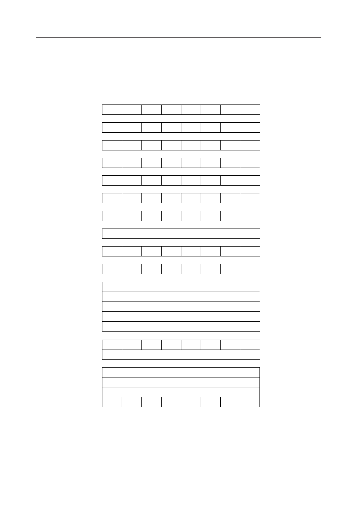
DETAILED DIAGRAM OF SPECIAL FUNCITON REGISTERS
Special
Function
Data
Address
0F0H B
(MSB) Bit Address (LSB)
F7 F6 F5 F4 F3 F2 F1 F0
E7 E6 E5 E4 E3 E2 E1 E00E0H ACC
CY AC F0 RS1 RS0 OV F1 P
D7 D6 D5 D4 D3 D2 D1 D00D0H PSW
PS PT1 PX1 PT0 PX0
— — — BC BB BA B9 B80B8H IP
B7 B6 B5 B4 B3 B2 B1 B00B0H P3
EA ES ET1 EX1 ET0 EX0
AF — — AC AB AA A9 A80A8H IE
Register
Symbol
A7 A6 A5 A4 A3 A2 A1 A00A0H P2
Not Bit Addressable99H SBUF
SM0 SM1 SM2 REN TB8 RB8 TI RI
9F 9E 9D 9C 9B 9A 99 9898H SCON
97 96 95 94 93 92 91 9090H P1
8DH TH1
8BH TL1
8AH TL0
89H TMOD
TF1 TR1 TF0 TR0 IE1 IT1 IE0 IT0
8F 8E 8D 8C 8B 8A 89 8888H TCON
82H DPL
81H SP
80H P0
87 86 85 84 83 82 81 80
Not Bit Addressable
Not Bit Addressable8CH TH0
Not Bit Addressable
Not Bit Addressable
Not Bit Addressable
Not Bit Addressable87H PCON
Not Bit Addressable83H DPH
Not Bit Addressable
Not Bit Addressable
11/38

¡ Semiconductor MSM80C31F/80C51F
INSTRUCTION LIST
List of Instruction Symbols
A : Accumulator
AB : Register pair
AC : Auxiliary carry flag
B : Arithmetic operation register
C : Carry flag
DPTR : Data pointer
PC : Program counter
Rr : Register indicator (r = 0 to 7)
SP : Stack pointer
AND : Logical product
OR : Logical sum
XOR : Exclusive-OR
+ : Addition
– : Subtraction
X : Multiplication
/ : Division
(X) : Denotes the contents of X
((X)) : Denotes the contents of address determined by the contents of X
# : Denotes the immediate data
@ : Denotes the indirect address
= : Equality
⫽ : Non-equality
¨ : Substitution
Æ : Substitution
— : Negation
< : Smaller than
> : Larger than
bit address : RAM and the special function register bit specifier address (b0 to b7)
code address : Absolute address (A0 to A15)
data : Immediate data (I0 to I7)
relative offset : Relative jump address offset value (R0 to R7)
direct address : RAM and the special function register byte specifier address (a0 to a7)
12/38
 Loading...