

Page 1

E2U0058-18-85
¡ Semiconductor
This version: Aug. 1998
MSM7719-01
¡ Semiconductor
MSM7719-01
Echo Canceler with ADPCM Transcoder
GENERAL DESCRIPTION
The MSM7719, developed for PHS (Personal Handyphone System) applications, is an LSI device
and contains a line echo canceler, an acoustic echo canceler (for handsfree conversation), and
a single channel full-duplex ADPCM transcoder.
This device includes DTMF tone and several types of tone generation, transmit/receive data mute
and gain control, and VOX function and is best suited for PHS applications.
FEATURES
• Single 5 V power supply VDD : 4.5 V to 5.5 V
• ADPCM : ITU-T Recommendations G.726
• PCM interface coding format : µ-law
• Built-in 2-channel (line and acoustic) echo canceler
Line echo canceler
Acoustic echo canceler (for handsfree conversation)
Echo attenuation : 30 dB (typ.)
Cancelable echo delay time :
27 ms (max.) for line echo canceler +27 ms (max.) for acoustic echo canceler
Line echo canceler mode only : 54 ms (max.)
• Serial PCM/ADPCM transmission data rate : 64 kbps to 2048 kbps
• Low supply current
Operating mode : Typically 50 mA (VDD = 5.0 V)
Power-down mode : Typically 0.2 mA (VDD = 5.0 V)
• Master clock frequency : 9.6 to 10.0 MHz/19.2 to 20.0 MHz
• Transmit/receive mute, transmit/receive programmable gain control
• Built-in DTMF tone generator and various tones generator
• Control through parallel microcontroller interface
Pin control available for line and acoustic echo cancelers
• Built-in VOX control
Transmit side : Voice/silence detect
Receive side : Background noise generation at the absence of voice signal
• Package:
100-pin plastic TQFP (TQFP100-P-1414-0.50-K) (Product name : MSM7719-01TS-K)
1/40
Page 2
¡ Semiconductor
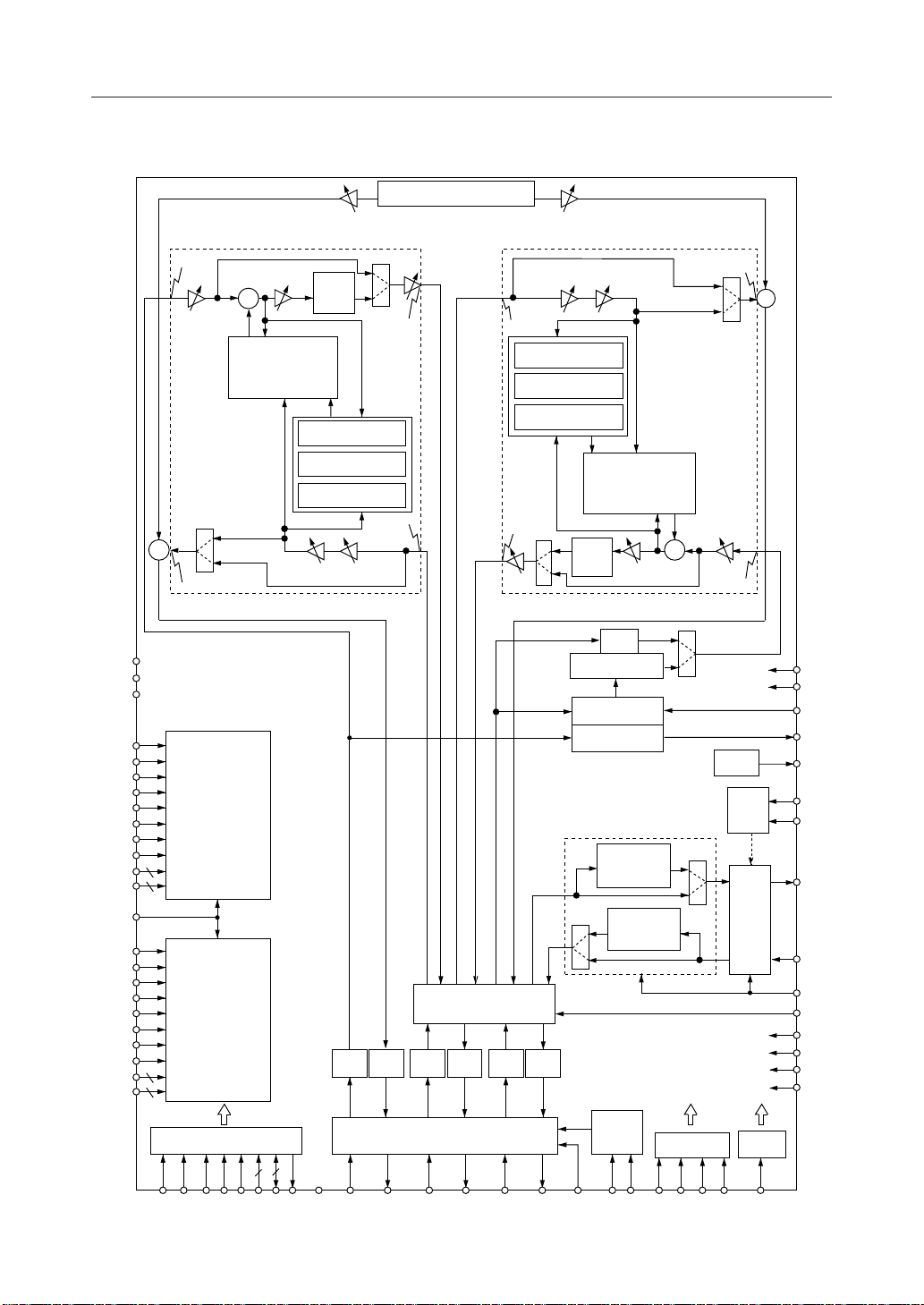
BLOCK DIAGRAM
MSM7719-01
DETSL
DETT
DETP
LTHR
LDCL
LCCL
LHD
LCLP
LHLD
LATT
LGC
LATTG2-0
LATTL2-0
+
SinL
ATTIL
RoutL
Line
Echo
Canceler
Controller
ATTtgrx
ATTsL
+
+
Line
Adaptive FIR Filter
(LAFF)
Howling Detector
Double Talk Detector
GainL ATTrL
Line Echo Canceler
Center
Clip
Power Calc.
Tone Generator (DTMF etc).
ATTgL
SoutL
RinL
ATTtgtx
ATTrA GainA
RinA
Power Calc.
Howling Detector
Double Talk Detector
SoutA
Center
Clip
ATTgA
Acoustic Echo Canceler
Power Detect
Voice Detect
ADPCM TRANSCODER
Acoustic
Adaptive FIR Filter
(AAFF)
ATTsA
Mute
Note Gen.
ADPCM
CODER
RoutA
+
ATTIA
–
+
+
SinA
MLV0-2
MUTE
VOXI
VOXO
VREF
Timing
Gen.
P/S
SG
BCLKA
SYNCA
IS
ECMODE
ATHR
ADCL
ACCL
AHD
ACLP
AHLD
AATT
AGC
AATTG2-0
AATTL2-0
Acoustic
Echo
Canceler
Controller
MTYPE
MCUSL
MCU I/F
CS
RD
WR
A4-0
D7-0
I/O Controller
N/L L/N N/L L/N N/L L/N
P/S&S/P
INT
PCMSL
PCMLNI
PCMLNO
PCMACI
PCMACO
PCMADI
PCMADO
DTHR
ADPCM
DECODER
Timing
Gen.
SYNCP
Clock Gen. Test I/F
MCK
BCLKP
MCKSL
PDN/RST
&
S/P
PDWN
TSTI1-6
IR
CONTA
IOSL0-1
V
DDD1-3
V
DDA
DG1-3
AG
2/40
Page 3
¡ Semiconductor
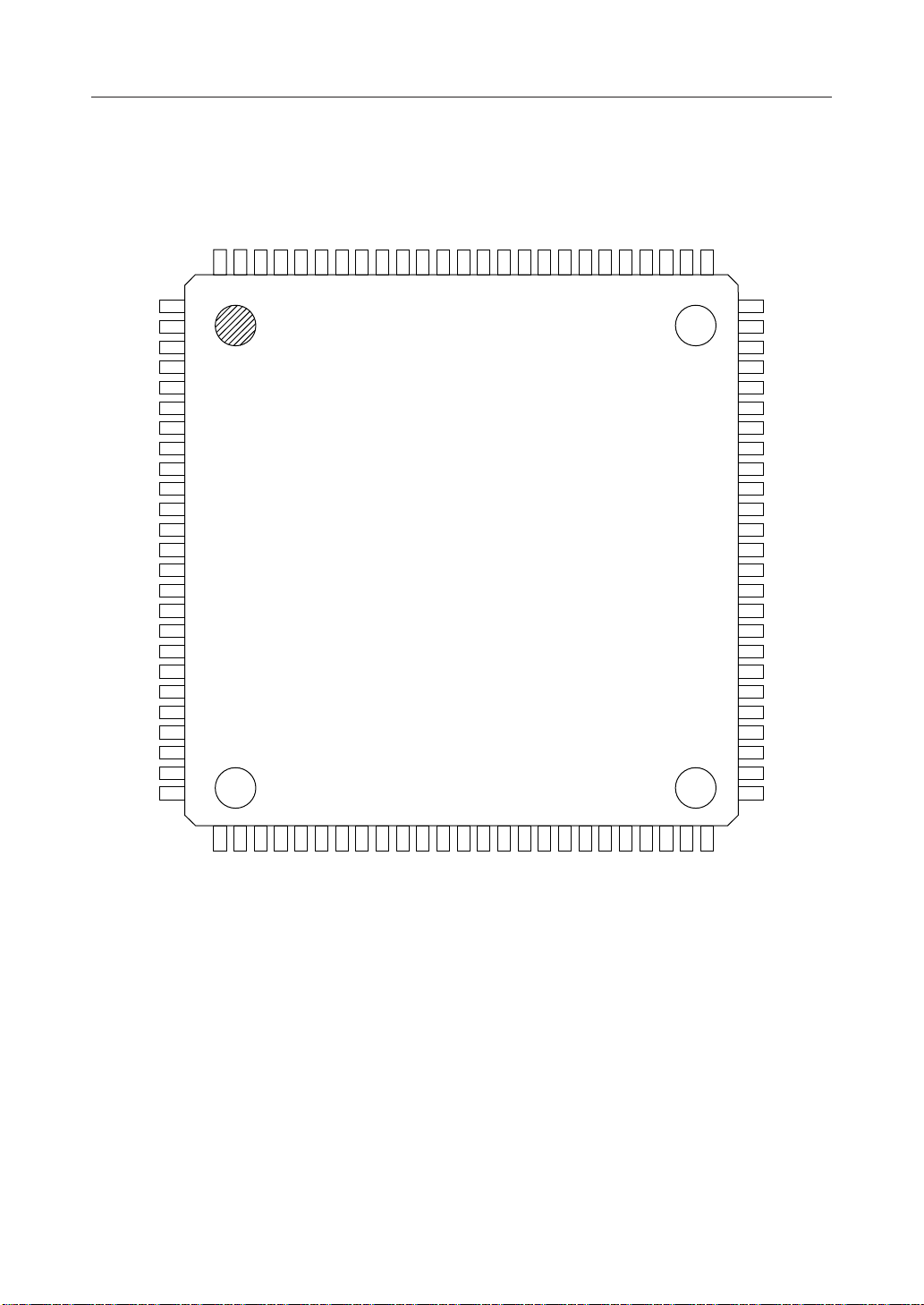
PIN CONFIGURATION (TOP VIEW)
MSM7719-01
DDD1
NC
DDD3
V
PDN/RST
SYNCA
SYNCP
D0
D1
D2
D3
D4
D5
D6
D7
NC
88
89
90
91
92
93
94
95
96
97
98
99
100
1
2WR
3RD
4A0
5A1
6A2
7V
8LDCL
9LCCL
10LHD
11LCLP
12DG1
13LHLD
14LATT
15LTHR
16LGC
17AGC
18ATHR
19AATT
20AHLD
21ACLP
22AHD
23ACCL
24ADCL
25NC
PDWN
87
TSTI1
86
INT
85
TSTI2
84
DETP
83
DG3
82
DETT
81
DETSL
80
ECMODE
79
IOSL1
78
IOSL0
77
NC
76
75
74
73
72
71
70
69
68
67
66
65
64
63
62
61
60
59
58
57
56
55
54
53
52
51
A4
CS
A3
VOX0
MCUSL
PCMSL
IS
PCMLN0
PCMAD0
PCMAC0
V
DDD2
MUTE
VOXI
TSTI6
TSTI5
BCLKP
BCLKA
MTYPE
DTHR
MLV0
MLV1
MLV2
AG
NC
NC
26
NC
28
27
LATTL1
LATTL2
30
29
LATTL0
LATTG2
36
35
34
33
32
31
DG2
AATTL0
AATTL1
AATTL2
LATTG0
LATTG1
NC: No-connect pin
100-Pin Plastic TQFP
38
37
AATTG1
AATTG2
40
39
AATTG0
PCMACI
42
41
IR
PCMADI
44
43
CONTA
PCMLNI
50
49
48
47
46
45
SG
DDA
V
TSTI4
TSTI3
MCK
MCKSL
3/40
Page 4

¡ Semiconductor
MSM7719-01
PIN FUNCTIONAL DESCRIPTION
SG
Outputs of the analog signal ground voltage.
The output voltage is approximately 2.4 V. Connect bypass capacitors of 10 mF and 0.1 mF
(ceramic type) between these pins and the AG pin. During power-down, the output changes
to 0 V.
AG
Analog ground.
DG1, 2, 3
Digital ground.
V
DDA
+5 V power supply for analog circuits.
V
DDD1, 2, 3
+5 V power supply for digital circuits.
PDN/RST
Power-down reset control input.
A logic “0” makes the LSI device enter a power-down state. At the same time, all control register
data are reset to the initial state. Set this pin to a logic “1” during normal operating mode. Since this pin
is ORed with CR0-B5 (bit 5 (B5) of control register CR0), set CR0-B5 to logic “0” when using this pin.
When this pin control is not used (i.e., when controlling by the control register), set this pin to logic
“1”.
PDWN
Power-down control input.
The device changes to the power-down state, and each bit of control register and internal variables
of control register are not reset when set to a logic “0”. During normal operation, set this pin to logic
“1”. Since this pin is ORed with CR0-B6 (bit 6 (B6) of control register CR0), set CR0-B6 to logic “0”
when using this pin. When this pin control is not used (i.e., when controlling by the control register),
set this pin to logic “1”.
MCK
Master clock input.
The frequency must be 9.6 to 10.0 MHz/19.2 to 20.0 MHz. The master clock signal is allowed to be
asynchronous with SYNCP, SYNCA, BCLKP, and BCLKA.
4/40
Page 5

¡ Semiconductor
MCKSL
Master clock selection input.
Set MCKSL to logic “0” when the master clock frequency is 9.6 to 10.0 MHz, and to logic “1”
when it is 19.2 to 20.0 MHz.
PCMACO
PCM data output of the echo canceler.
PCM is output from MSB in a sequential order, synchronizing with the rising edge of BCLKP and
SYNCP.
This pin is in a high impedance state except during 8-bit PCM output. When DTHR is set to logic
“1”, this pin becomes a 4-bit output and the input data to the input pin set by IOSL0-1 is output as
it is. In this case, this pin is in a high impedance state except during 4-bit output. Note that the echo
canceler signal output mode for this pin changes depending on the setting of IOSL0-1. (This pin is
also in a high impedance state during power-down or initial mode.)
Refer to Figs. 1-5.
PCMACI
PCM data input of the echo canceler.
PCM is shifted in at the falling edge of BCLKP and input from MSB.
The start of the PCM data (MSB) is identified at the rising edge of SYNCP. When DTHR is set to logic “1”,
this pin becomes a 4-bit input and the input data is output to the output pin set by IOSL0-1 as it is.
This pin is provided with a 500-kW pull-up resistor. Note that the echo canceler signal input mode
for this pin changes depending on the setting of IOSL0-1.
Refer to Figs. 1-5.
MSM7719-01
PCMADO
PCM data output.
PCM is serially output from MSB in synchronization with the rising edge of BCLKP and SYNCP.
This pin is in a high impedance state except during 8-bit PCM output. When DTHR is set to logic
“1”, this pin becomes a 4-bit output and the input data to the input pin set by IOSL0-1 is output as
it is. In this case, this pin is in a high impedance state except during 4-bit output.
Note that the signal ouput mode for this pin changes and the I/O control signal for this pin switches
between BCLKA/SYNCA and BCLKP/SYNCP depending on the setting of IOSL0-1. (This pin is
also in a high impedance state during power-down or initial mode.)
Refer to Figs. 1-5.
PCMADI
PCM data input.
PCM is shifted in at the falling edge of the BCLKP signal and input from MSB. The start of the PCM
data (MSB) is identified at the rising edge of SYNCP. When DTHR is set to logic “1”, this pin becomes
a 4-bit input and the input data is output to the output pin set by IOSL0-1 as it is. This pin is provided
with a 500-kW pull-up resistor. Note that the signal input mode for this pin changes and the I/O
control signal for this pin switches between BCLKA/SYNCA and BCLKP/SYNCP depending on
the setting of IOSL0-1.
Refer to Figs. 1-5.
5/40
Page 6

¡ Semiconductor
IOSL0-1
These pins specify PCM signal I/O mode for the PCMACO, PCMACI, PCMADO, and PCMADI
pins. Since The IOSL0 and IOSL1 pins are ORed with the control register bits CR3-B6 and B5, set
these bits to logic “0” before using these pins. When this pin control is not used (i.e., in the case of
control with the control register), set these pins to logic “0”.
Refer to Figs. 1-5.
IS
Transmit ADPCM data output.
This data is serially output from MSB in synchronization with the rising edge of BCLKA and SYNCA.
This pin is in a high impedance state except during 4-bit ADPCM output. When CONTA is set to
logic
“1”, this pin becomes an 8-bit output and the data that passed through the ADPCM
is output. In this case, this pin is in a high impedance state except during 8-bit output.
(This pin is also in a high imedance state during power-down or initial mode.)
Refer to Figs. 1-5.
IR
Receive ADPCM data input.
ADPCM is shifted in on the rising edge of BCLKA in synchronization with SYNCA and input
data orderly from MSB. When CONTA is set to logic “1”, this pin becomes an 8-bit input and the
data is passed through the ADPCM transcoder and processed. This pin is provided with a 500-kW
pull-up resistor.
MSM7719-01
transcoder
PCMLNO
PCM receive data output of the line echo canceler.
PCM is output from MSB in a sequential order, synchronizing with the rising edge of BCLKP and
SYNCP.
This pin is in a high impedance state except during 8-bit PCM output. When DTHR is set to logic
“1”, this pin becomes a 4-bit output and the input data to the input pin set by IOSL0-1 is output as
it is. In this case, this pin is in a high impedance state except during 4-bit output.
(This pin is also in a high impedance state during power-down or initial mode.)
Refer to Figs. 1-5.
PCMLNI
PCM transmit data input of the line echo canceler.
PCM is shifted in at the falling edge of the BCLKP signal and input from MSB. The start of the PCM
data (MSB) is identified at the rising edge of SYNCP. When DTHR is set to logic “1”, this pin becomes
a 4-bit input and the input data is output to the output pin set by IOSL0-1 as it is. This pin is provided
with a 500-kW pull-up resistor.
Refer to Figs. 1-5.
6/40
Page 7

¡ Semiconductor
BCLKA
Shift clock input for the ADPCM data (IS, IR).
The frequency is from 64 kHz to 2048 kHz.
SYNCA
8 kHz synchronous signal input for ADPCM data.
Synchronize this data with BCLKA signal. SYNCA is used for indicating the MSB of the serial
ADPCM data stream.
BCLKP
Shift clock input for the PCM data (PCMLNO/PCMLNI, PCMACO/PCMACI, PCMADO/
PCMADI). The frequency is set in the range of 64 kHz to 2048 kHz.
SYNCP
8 kHz synchronous signal input for PCM data.
This signal must be synchronized with the BCLKP signal.
MCUSL, MTYPE
MSM7719-01
If the microcontroller interface is not to be used, set the MCUSL input pin to logic “1”. This setting
skips the intitial mode as the operating mode. For the MTYPE pin, which is the microcontroller
interface selection pin, logic “0” sets the read/write independent control mode and logic “1” sets
read/write shared control mode.
When this pin control is not used (i.e., when controlling by the control register), set these pins to logic
“0”.
CS, RD, WR
A 19-byte control register is provided in this LSI device. Data is read and written by using these pins
from the external microcontroller. See the microcontroller write and read timing diagrams in the
Electrical Characteristics.
When this pin control is not used (i.e., when controlling by the control register), set these pins to logic
“1”.
A4-A0, D7-D0
A4-A0 are address input pins of the control register, and D7-D0 are data I/O pins.
When this pin control is not used (i.e., when controlling by the control register), set these pins to logic
“0”.
INT
Reserved.
PCMSL
Reserved.
7/40
Page 8
¡ Semiconductor
MSM7719-01
CONTA
ADPCM transcoder setting pin. When this pin is set to logic “1”, the transcoder-through mode is
set. In this mode, the IS and IR pins become 8-bit PCM serial input and output pins. Since this pin
is ORed with the control register bit CR1-B7, set CR1-B7 to logic “0” to use this pin.
When this pin control is not used (i.e., when controlling by the control register), set this pin to logic
“0”.
Refer to Figs. 1-5.
DTHR
Through mode setting pin. When this pin is set to logic “1”, the entire circuit is put in the through
mode. In this mode, the PCM input and output pins become 4-bit serial input and output pins and
all functions of the echo canceler, ADPCM transcoder, and MUTEVOX are disabled. Use this pin
when making 32-kbps data communication.
Since this pin is ORed with the control register bit CR1-B5, set CR1-B5 to logic “0” to use this pin.
When this pin control is not used (i.e., when controlling by the control register), set this pin to logic
“0”.
Note that 64-kbps data communication is not supported in this device.
Refer to Figs. 1-5.
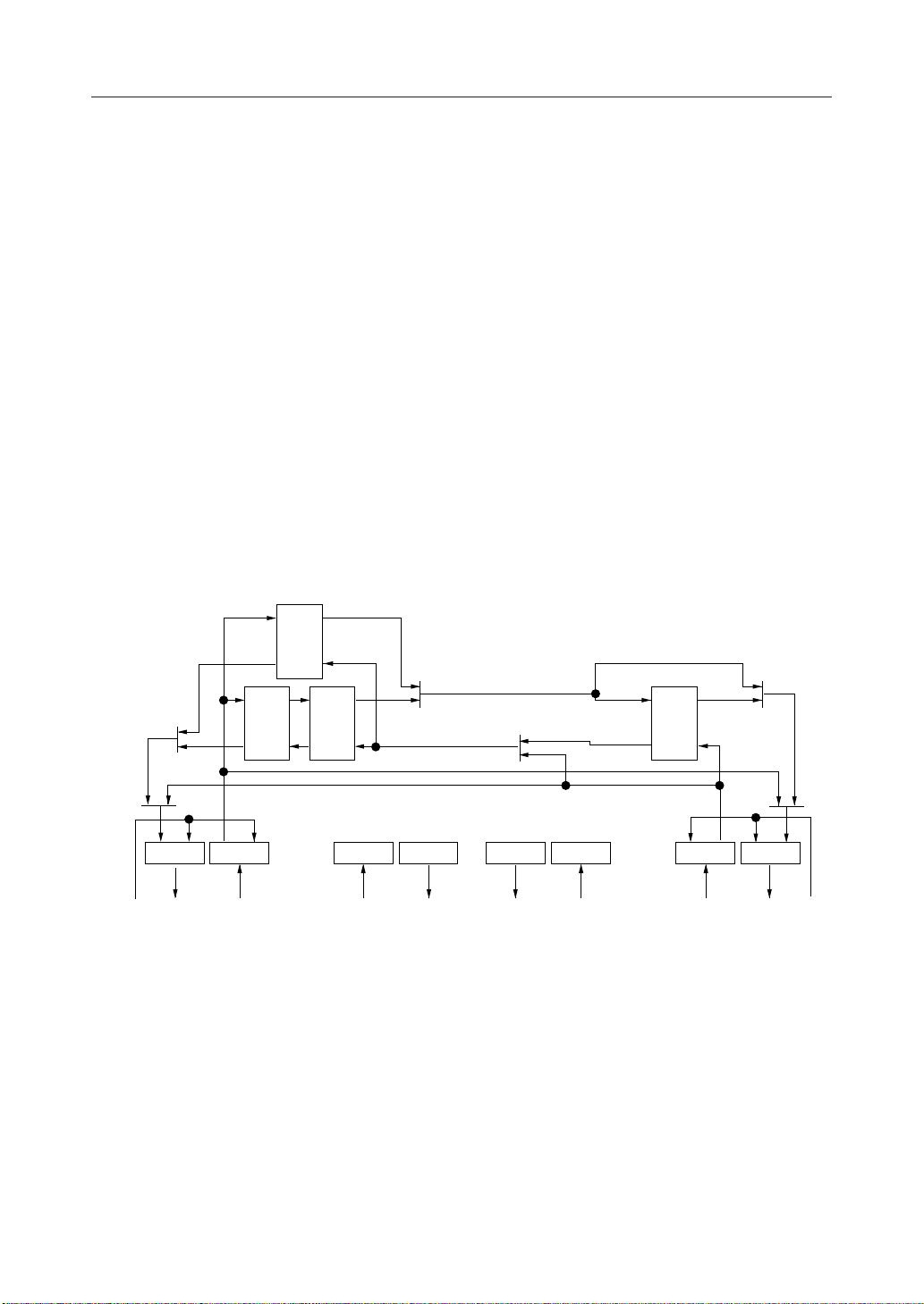
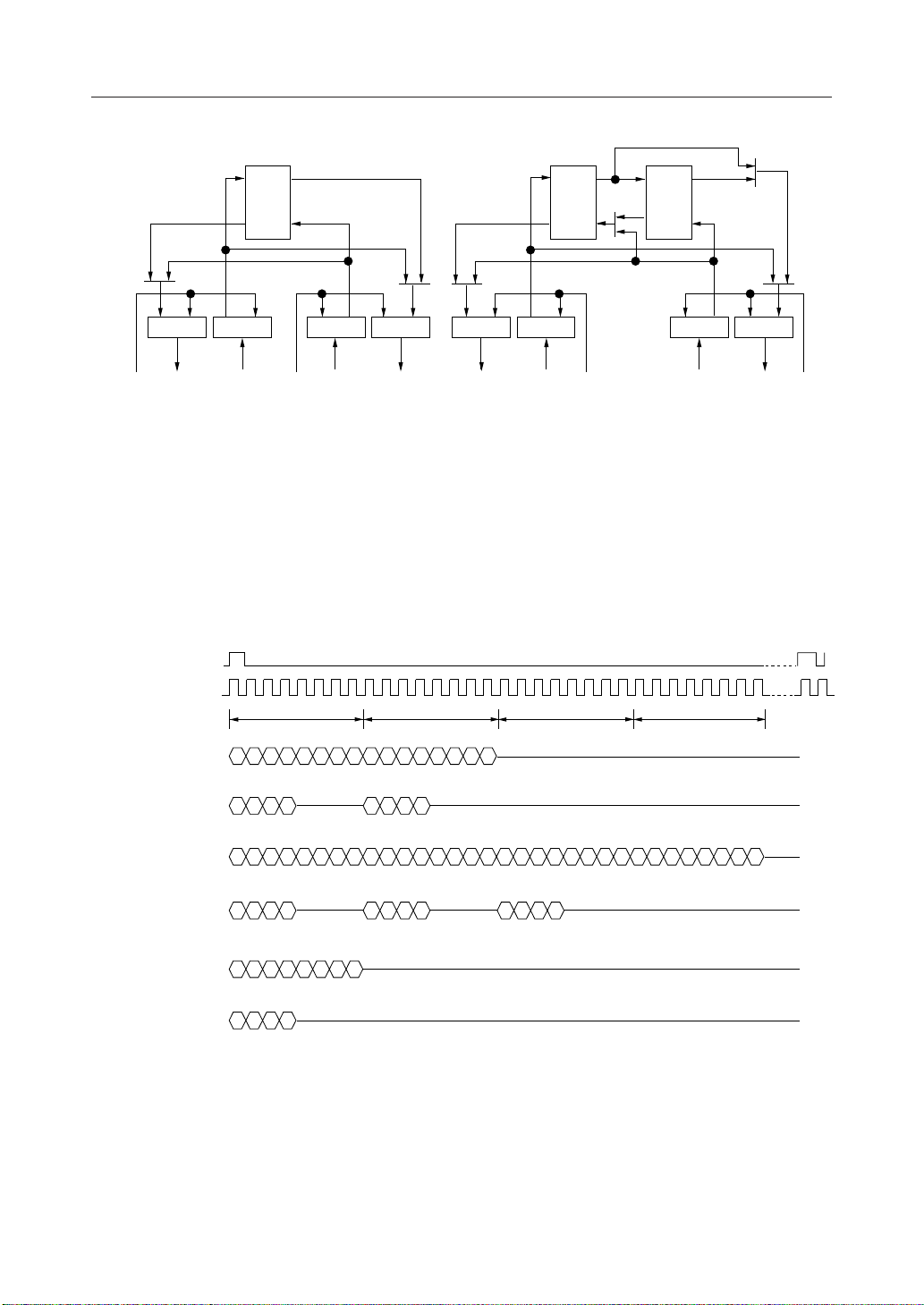
SYNCP
BCLKP
CR2-B3, B2
Echo
Canceler
(54ms)
(a)
(c)
Output Control Input Control Input Control Output Control Output Control Input Control Input Control Output Control
PCMLNO PCMACI PCMACO PCMADOPCMLNI PCMADI IR IS SYNCA
Line
Echo
Canceler
(27ms)
(c)(c)
Acoustic
Echo
Canceler
(27ms)
(a)
(b)
ADPCM
Transcoder
(b) (b)
(b)
(c)
BCLKA
Figure 1 Signal I/O Control 1
IOSL1="0", IOSL0="0"
Control (a): ECMODE, CR0-B0
Control (b): CONTA, CR1-B7
Control (c): DTHR, CR1-B5
8/40
Page 9
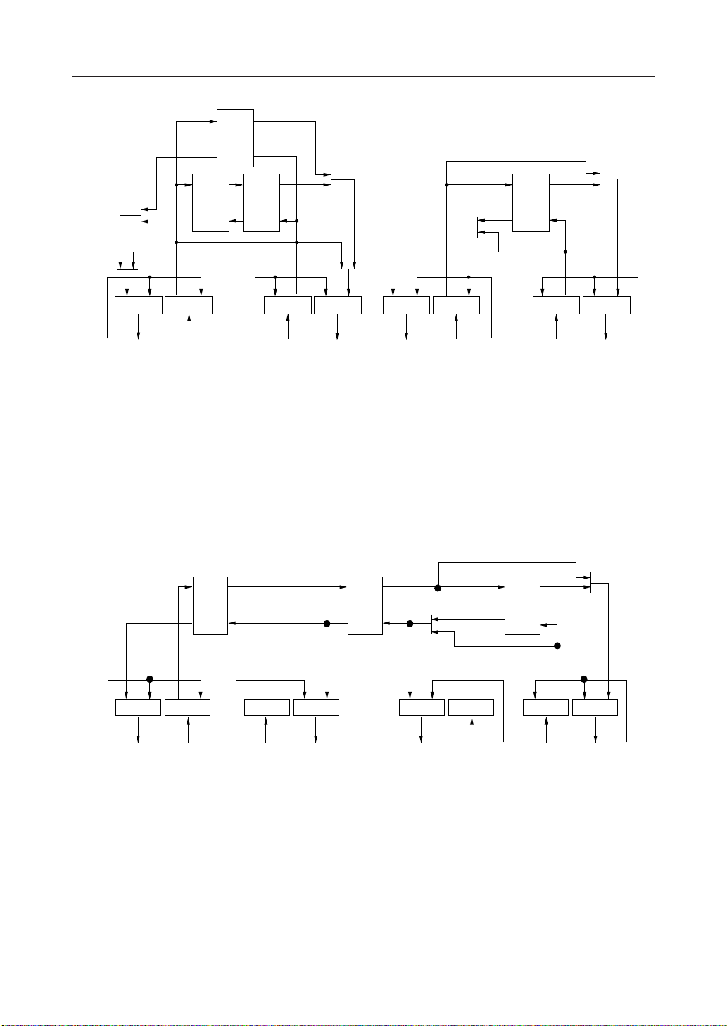
¡ Semiconductor
Line
(a)
Echo
Canceler
(27ms)
Echo
Canceler
(54ms)
Acoustic
Echo
Canceler
(27ms)
(a)
(b)
MSM7719-01
(b)
ADPCM
Transcoder
(c)
Output Control Input Control Output Control Input Control Input Control Output Control
Input Control Output Control
(c)
(c) (c) (c) (c) (b) (b)
SYNCP
BCLKP
CR2-B3, B2
PCMLNO PCMLNI IR IS SYNCA
SYNCP
BCLKP
CR2-B1, B0
PCMACI PCMACO PCMADO PCMADI SYNCP
BCLKP
CR2-B4
Figure 2 Signal I/O Control 2
IOSL1="0", IOSL0="1"
Control (a): ECMODE, CR0-B0
Control (b): CONTA, CR1-B7
Control (c): DTHR, CR1-B5
Line
Echo
Canceler
(27ms)
Acoustic
Echo
Canceler
(27ms)
ADPCM
Transcoder
(b)
BCLKA
(b)
SYNCP
BCLKP
CR2-B3, B2
Output Control Input Control Input Control Output Control Output Control Input Control Input Control Output Control
(b) (b)
PCMLNO
PCMLNI
SYNCP
BCLKP
CR2-B1, B0
PCMACI PCMACO
PCMADO
PCMADI
SYNCP
BCLKP
CR2-B4
IR IS
Figure 3 Signal I/O Control 3
IOSL1="1", IOSL0="0"
Control (a): ECMODE, CR0-B0
Control (b): CONTA, CR1-B7
Control (c): DTHR, CR1-B5
SYNCA
BCLKA
9/40
Page 10
¡ Semiconductor
,
,
(
)
MSM7719-01
(b)
Line
Echo
Canceler
(27ms)
(c) (c) (c) (c) (c) (c)
SYNCP
BCLKP
CR2-B3
PCMLNO PCMACI PCMACO PCMADOPCMLNI PCMADI IR IS SYNCA
B2
SYNCP
BCLKP
CR2-B1
B0
Figure 4 Signal I/O Control 4
SYNCP/SYNCA
BCLKP/BCLKA
PCM multiplexing
PCMADI/O data
(DTHR="0")
PCMADI/O data
(DTHR="1")
time slot 1
12345678 23456781
MSB
1234 1234
MSB
time slot 2 time slot 3 time slot 4
Acoustic
Echo
Canceler
(27ms)
(c)(c)(c)
Output Control Input ControlInput Control Output ControlOutput Control Input Control
(b)
ADPCM
Transcoder
(c)
Input Control Output Control
(b) (b)
SYNCA
BCLKA
CR2-B4
BCLKA
IOSL1="1", IOSL0="1"
Control (a): ECMODE, CR0-B0
Control (b): CONTA, CR1-B7
Control (c): DTHR, CR1-B5
PCMLNI/O data
PCMACI/O data
(DTHR="0")
PCMLNI/O data
PCMACI/O data
(DTHR="1")
IR/IS data
(CONTA="1")
IR/IS data
CONTA="0"
12345678 23456781 12345678 23456781
MSB
1234 1234 1234
MSB
12345678
MSB
1234
MSB
Note: The PCM signals (PCMADI and PCMADO) of the ADPCM transcoder can be assigned to
time slot 1 or 2.
The PCM signals (PCMLNI, PCMLNO, PCMACI, and PCMACO) of the echo canceler can
be assigned to one of the time slots 1 to 4.
The ADPCM signals (IR and IS) of the ADPCM transcoder are always assigned to time slot
1.
Figure 5 PCM Multiplexing/ADPCM Timing
10/40
Page 11

¡ Semiconductor
ECMODE
This pin specifies the operating mode of the echo canceler. When set to logic “0”, this device
operates as a line echo canceler (with cancelable echo delay time of 27 ms max.) + an acoustic echo
canceler (with cancelabel echo delay time of 27 ms max.); when set to logic “1”, it operates as a line
echo canceler (with cancelable echo delay time of 54 ms max.).
When this pin control is not used (i.e., when controlling by the control register), set these pins
to logic “0”.
LTHR, ATHR
(L: Line A: Acoustic)
These pins control the through mode of the echo canceler. In this mode, SinL/A data and RinL/A
data is output directly to SoutL/A and RoutL/A respectively, while retaining their echo canceler
coefficients.
0: Normal mode (Echo cancellation) 1: Through mode
When this pin control is not used (i.e., when controlling by the control register), set these pins to logic
“1”.
LDCL, ADCL
These pins control clearing the coefficient 1 of the adaptive FIR filter used by the echo canceler. If
the echo path changes, reset both the coefficient 1 (by setting LDCL/ADCL to “0”) and the coefficient
2 (by setting LCCL/ACCL to “0”) of the adaptive FIR filter whenever possible.
0: Resets the coefficient 1: Normal operation
When this pin control is not used (i.e., when controlling by the control register), set these pins to logic
“1”.
MSM7719-01
LCCL, ACCL
These pins control clearing the coefficient 2 of the adaptive FIR filter used by the echo canceler. If
the echo path changes, reset both the coefficient 1 (by setting LDCL/ADCL to “0”) and the coefficient
2 (by setting LCCL/ACCL to “0”) of the adaptive FIR filter whenever possible.
0: Resets the coefficient 1: Normal operation
When this pin control is not used (i.e., when controlling by the control register), set these pins to logic
“1”.
LHD, AHD
Howling detection ON/OFF control pins.
0: OFF, 1: ON
When this pin control is not used (i.e., when controlling by the control register), set these pins to logic
“0”.
LCLP, ACLP
These pins turn ON or OFF the Center Clipping funciton that forcibly sets the SoutL output of the
line echo canceler to minimum positive value when it is –57 dBm0 or less.
0: Center Clipping OFF
1: Center Clipping ON
When this pin control is not used (i.e., when controlling by the control register), set these pins to logic
“0”.
11/40
Page 12

¡ Semiconductor
LHLD, AHLD
These pins control updating the coefficient of the adaptive FIR filter (AFF) for the echo canceler.
0: Normal mode (updates the coefficient)
1: Coefficient Fixed mode
When this pin control is not used (i.e., when controlling by the control register), set these pins to logic
“0”.
LATT, AATT
These pins turn ON or OFF the ATT function that prevents howling from occurring by means of
attenuators ATTsL/A and ATTrL/A provided for the RinL/A input and the SoutL/A output of the
echo canceler.
When a signal is input to RinL/A only, the attenuator ATTsL/A of the SoutL/A output is activated.
When a signal is input to SinL/A only or to both SinL/A and RinL/A, the attenuator ATTrL/A of
the RinL/A input is activated. The ATT values are both about 6 dB.
0: ATT function ON
1: ATT function OFF
When this pin control is not used (i.e., when controlling by the control register), set these pins to logic
“0”.
LGC, AGC
MSM7719-01
These pins turn ON or OFF the gain control function that controls the RinL/A input level and
prevents howling from occurring by the gain controller (GainL/A) provided for the RinL/A input
of the echo canceler. The RinL/A input level is adjusted in the attenuation range of 0 to –8.5 dB.
This adjusting starts at the RinL/A input level of –24 dBm0.
0: gain control OFF
1: gain control ON
When this pin control is not used (i.e., when controlling by the control register), set these pins to logic
“0”.
MUTE
Receive side voice path mute level enable pin. To set a mute level, set this pin to logic “1”.
When this pin control is not used (i.e., when controlling by the control register), set this pin to logic
“0”.
MLV0-2
Receive side voice path mute level setting pins. For the control method, refer to the control register
(CR1) description. Since this signal is ORed with CR1-B2, B1, and B0 internally, set the bits of the
register to logic “0” before using these pins.
DETSL
Reserved pin.
Set this pin to logic “0”.
12/40
Page 13

¡ Semiconductor
DETT
Reserved pin.
Set this pin to logic “0”.
DETP
Reserved pin.
Set this pin to logic “0”.
LATTG2-0, AATTG2-0
Pad setting pins for the echo canceler's SoutL/A output gain.
Level ATTG2 ATTG1 ATTG0
0 dB 0 0 0
2 dB 0 0 1
4 dB 0 1 0
6 dB 0 1 1
8 dB 1 0 0
10 dB 1 0 1
12 dB 1 1 0
14 dB 1 1 1
MSM7719-01
When this pin control is not used (i.e., when controlling by the control register), set these pins to logic
“0”.
LATTL2-0, AATTL2-0
Pad setting pins for the echo canceler's SinL/A input loss.
Level ATTL2 ATTL1 ATTL0
–0 dB 0 0 0
–2 dB 0 0 1
–4 dB 0 1 0
–6 dB 0 1 1
–8 dB 1 0 0
–10 dB 1 0 1
–12 dB 1 1 0
–14 dB 1 1 1
When this pin control is not used (i.e., when controlling by the control register), set these pins to logic
“0”.
TSTI1-6
Test input pins.
Tie to logic “0”.
13/40
Page 14

¡ Semiconductor
MSM7719-01
VOXO
Signal outut for transmit side VOX function.
This pin is effective when CR6-B7 is set to logic “1” (VOX ON).
The VOX function recognizes the presence or absence of the transmit voice signal by detecting the
level of the transmit signal to the line echo canceler. “1” and “0” levels set to this pin correspond to
the presence and the absence of voice, respectively. This result appears also at the register bit CR7B7. The signal energy detect threshold is set by the control register bits CR6-B6, B5.
The timing diagram of the VOX function is shown in Figure 3.
The transmit signal to the line echo canceler refers to the signal input to the PCMLNI pin.
Refer to Figure 6.
VOXI
Signal input for receive side (acoustic echo canceler Sin side) VOX function.
The “1” level at VOXI indicates the presence of a voice signal, the decoder block processes normal
receive signal, and the voice signal on the PCMACI pin goes through. The “0” level indicates the
absence of a voice signal and the background noise generated in this device is output.
The background noise amplitude is set by the control register CR6.
Because this signal is ORed with the register bit CR6-B3, set CR6-B3 to logic “0” when using this
pin.
When this pin control is not used (i.e., when controlling by the control register), set this pin to logic
“0”.
Refer to Figure 6.
Transmit Signal
PCMLNI
(shown as an
analog signal)
VOXO
VOXI
Receive Signal
Acoustic Echo
Canceler Sin
(shown as an
analog signal)
T
VXON
Voice
Detect
Voice Silence Voice
T
VXOFF
Silence
Detect (Hangover time)
(a) Transmit Side VOX Function Timing Diagram
Voice Silence Voice
Receive Signal
Decoded Time Period
(b) Receive Side VOX Function Timing Diagram
Figure 6 VOX Function
Background
Noise
14/40
Page 15

¡ Semiconductor
ABSOLUTE MAXIMUM RATINGS
MSM7719-01
Parameter
Power Supply Voltage
Digital Input Voltage
Digital Output Voltage
Storage Temperature
Symbol
V
DD
V
DIN
V
OUT
T
STG
Condition
—
—
—
—
Rating
–0.3 to +7.0
–0.3 to V
–0.3 to V
–55 to +150
DD
DD
+ 0.3
+ 0.3
Unit
V
V
V
°C
RECOMMENDED OPERATING CONDITIONS
(VDD = 4.5 V to 5.5 V, Ta = –25°C to +70°C)
Parameter
Power Supply Voltage
Operating Temperature
Input High Voltage
Input Low Voltage
Digital Input Rise Time
Digital Input Fall Time
Master Clock Frequency
Master Clock Duty Ratio
Bit Clock Frequency
Synchronous Pulse Frequency (*1)
Clock Duty Cycle (*2)
Transmit Sync Pulse Setting Time
Receive Sync Pulse Setting Time
Receive Sync Pulse Setting Time
PCM, ADPCM Set-up Time
PCM, ADPCM Hold Time
Symbol
V
DD
Ta
V
IH
V
IL
t
Ir
t
If
f
MCK
D
C
f
BCK
f
SYNC
D
CK
t
XS
t
SX
t
XO
t
RS
t
SR
t
RO
t
WS
t
DS
t
DH
Condition
—
—
All digital inputs
All digital inputs
All digital inputs
Measurement point=0.8V&2.4V
MCK (When MCKSL="1")
MCK (When MCKSL="0")
MCK
BCLKP, BCLKA
SYNCP, SYNCA
BCLKP, BCLKA
BCLKP to SYNCP,
BCLKA to SYNCA
SYNCP to BCLKP,
SYNCA to BCLKA
SYNCP to BCLKP,
SYNCA to BCLKA
BCLKP to SYNCP,
BCLKA to SYNCA
SYNCP to BCLKP,
SYNCA to BCLKA
SYNCP to BCLKP,
SYNCA to BCLKA
SYNCP, SYNCA
—
—
Min.
+4.5
–25
2.4
0
—
—
–
100 ppm
40
64
—
40
100
100
100
100
1 BCLK
100
100
Typ.
—
+25
—
—
—
—
19.2-20.0
9.6-10.0
50
—
8.0
50
—
—
——
—
—
——
—
—
—
*1 If SYNCP and SYNCA are generated from different clocks, be sure to keep the relative
timing of the rising edges of SYNCP and SYNCA (that is, which rising edge is earlier) after
releasing the reset.
*2 The recommended condition (values) for the clock duty cycle need not be observed if the clock
duty cycle fulfills the digital interface timing.
Max.
+5.5
+70
+0.3
V
DD
0.8
5
5
+100 ppm
60
2048
—
60
—
—
100
—
—
100
100
—
—
Unit
V
°C
V
V
ns
ns
MHz
%
kHz
kHz
%
ns
ns
ns
ns
ns
ns
ms
ns
ns
15/40
Page 16

¡ Semiconductor
ELECTRICAL CHARACTERISTICS
DC Characteristics
Parameter Symbol Condition Min. Typ. Max. Unit
Power Supply Current 1
Power Supply Current 2
Input Leakage current
High Level Digital
Output Voltage
Low Level Digital
Output Voltage
Digital Output
Leakage Current
Input Capacitance
Operating mode, no signal
I
DD1
(V
DD
Power down mode
I
DD2
(VDD=5 V, only the master clock is input)
I
VI= V
IL
V
IOH= –0.4 nA
OH
I
V
OL
I
LO
C
IN
OL
V
I=VDD
=3.2 mA
=5 V)
DD
/0 V
—
MSM7719-01
= 4.5 to 5.5 V, Ta = –25 to +70°C)
(V
DD
—5080mA
— 0.2 1 mA
–10 — +10 mA
4.2 — V
0 0.2 0.4 V
——10mA
—5—pF
DD
V
Analog Interface Characteristics
(V
= 4.5 to 5.5 V, Ta = –25 to +70°C)
DD
Parameter Symbol Condition Min. Typ. Max. Unit
SG Output Voltage
SG Output Impedance
V
SG
SG
R
SG
SG
2.35 2.4 2.45
—4080
V
kW
Reset Timing
(V
= 4.5 to 5.5 V, Ta = –25 to +70°C)
DD
Parameter
Reset Signal Width
Reset Start Time
Reset Termination Time
Symbol
t
RSTW
t
RSTS
t
RSTE
Condition Min.
—
—
—
1
—— 1ms
— — 200 ms
Typ.—Max.—Unit
ms
Note: Values in the table are common to the PDN/RST pin and the control register bit CR0-B5.
• Reset timing
t
RSTW
PDN/RST
Internal
Processing
t
RSTS
Reset Initial mode
t
RSTE
16/40
Page 17

¡ Semiconductor
p
MSM7719-01
Echo Canceler Coefficient Reset Timing
(V
= 4.5 to 5.5 V, Ta = –25 to +70°C)
DD
Parameter
Echo Canceler Reset Signal Width
Echo Canceler Reset Detection Time
Echo Canceler Reset Operating Time t
Symbol
t
ECRSTW
t
ECRSTD
ECRST
Condition Min.
—
—
—
125
0 — 125 ms
— — 125 ms
Typ.—Max.—Unit
ms
Note: Values in the table are common to the PDN/RST pin and the control register bit CR0-B5.
• Echo canceler coefficient reset timing
LDCL
t
ECRSTW
ADCL
LCCL
t
ECRSTD
ACCL
Detect
(8 kHz sampling)
Coefficient reset processing (t
Note : In the above timing, the LDCL, ADCL, LCCL, and ACCL register bits are active high, and
the LDCL, ADCL, LCCL, and ACCL
Control Pin Timing
Parameter
Control Signal Width
Control Signal Detection Time
Operation Start Time
Symbol
t
SETUPW
t
SETUPD
t
SETUPS
Condition Min.
—
—
—
Note: The control pins / register bits are as follows:
DETSL, DETT, DETP, (A/L)THR, (A/L)DCL, (A/L)CCL, (A/L)HLD, (A/L)ATT, (A/L) GC,
(A/L)ATTG2-0, (A/L)ATTL2-0, PCMSL, DTHR, IOSL0-1, CINTA, MUTE, MLV0-2
t
ECRSTD
)
ECRST
ins are active low.
(V
DD
125
Echo canceler operatingReset
= 4.5 to 5.5 V, Ta = –25 to +70°C)
Typ.—Max.—Unit
ms
0 — 125 ms
0 — 125 ms
• Control pin timing
Control Pin
Detect
(8 kHz sampling)
t
SETUPD
t
SETUPS
t
SETUPW
t
SETUPD
t
SETUPS
Internal Processing Internal ProcessingInternal Processing
17/40
Page 18

¡ Semiconductor
Digital Interface Characteristics
Parameter Symbol Condition Min. Typ. Max. Unit
Digital Output Delay Time
PCM, ADPCM Interface
t
t
t
t
SDX
XD1
XD2
XD3
, t
SDR
, t
RD1
, t
RD2
, t
RD3
• PCM/ADPCM output timing
—
MSM7719-01
= 4.5 to 5.5 V, Ta = –25 to +70°C)
(V
DD
0—
0—
0—
0—
100
100
100
100
ns
ns
ns
ns
BCLKP
SYNCP
PCMO
BCLKA
0
t
XS
High-Z High-Z
t
t
XS
12345678910
t
SX
t
XD1
t
XO
t
t
MSB LSB
SDX
123456789100
t
SX
SYNCA
t
XD1
t
XO
IS
t
SDX
t
MSB LSB
• PCM/ADPCM input timing
BCLKA
SYNCA
0 10
t
RS
123456789
t
SR
t
RO
DS
WS
XD2
XD2
t
XD3
t
XD3
t
WS
High-ZHigh-Z
tDHt
IR
BCLKP
SYNCP
PCMI
MSB
123456789100
t
t
SR
RO
MSB
t
DS
t
RS
t
WS
t
DH
LSB
LSB
18/40
Page 19

¡ Semiconductor
MSM7719-01
AC Characteristics (Gain Settings)
(V
= 4.5 to 5.5 V, Ta = –25 to +70°C)
DD
Parameter Symbol Condition Min. Typ. Max. Unit
Transmit/Receive Gain
Setting Accuracy
D
For all gain set values –1 0 +1 dB
G
AC Characteristics (VOX Function)
(V
= 4.5 to 5.5 V, Ta = –25 to +70°C)
DD
Parameter Symbol Condition Min. Typ. Max. Unit
VOXO pin:see Fig.6
Voice/silence
differential:10 dB
140/300 160/320 180/340 ms
–2.5 0 +2.5 dB
(Voice Signal ON/OFF Detect Time)
Transmit VOX Detection Level
Accuracy (Voice Detection Level)
t
VXON
t
VXOFF
D
SilenceÆvoice — 5 — msTransmit VOX Detection Time
VoiceÆsilence
For detection level set values by
VX
CR6-B6,B5
AC Characteristics (DTMF and Other Tones)
(V
= 2.7 to 3.6 V, Ta = –25 to +70°C)
DD
Parameter Symbol Condition Min. Typ. Max. Unit
Frequency Deviation
Tone Reference
Output Level
(*1)
Relative Value of
DTMF Tones
R
Df
Df
V
TL
V
TH
V
RL
V
RH
DTMF
T1
T2
Transmit side tone
(Gain set value:0dB)
Receive side tone
(Gain set value:0dB)
V
TH/VTL, VRH/VRL
DTMF Tones
Other various tones
DTMF (Low group)
DTMF (High group), Others
DTMF (Low group)
DTMF (High group), Others
–1.5 — +1.5 %
–1.5 — +1.5 %
–10 –8 –6 dBm0
–8 –6 –4 dBm0
–10 –8 –6 dBm0
–8 –6 –4 dBm0
123dB
*1 Not including programmable gain set values
19/40
Page 20

¡ Semiconductor
Microcontroller Interface (WR and RD Pins Controlled Independently)
= 4.5 to 5.5 V, Ta = –25 to +70°C)
(V
DD
Parameter
Address and Chip Select Setup Time
(with respect to the falling edge of WR)
Address and Chip Select Setup Time
(with respect to the rising edge of WR)
WR Pulse Width t
Data Input Setup Time
Data Input Hold Time
Address and Chip Select Setup Time
(with respect to the falling edge of RD)
Address and Chip Select Setup Time
(with respect to the rising edge of RD)
RD Pulse Width
Data Output Setup Time
Data Output Hold Time
Symbol
t
CWS
t
CWH
WW
t
DWS
t
DWH
t
CRS
t
CRH
t
RW
t
DOD
t
DOH
Condition Min.
30——
15——
45——
30
MTYPE=0
15
30
15——
45——
——40
0——
Typ.
MSM7719-01
—
—
—
Max.
—
—
—
Unit
ns
• Microcontroller write timing (WR and RD controlled independently)
A4-0
CS
t
CWS
t
WW
t
CWH
WR
D7-0
High-Z High-Z
t
DWStDOH
• Microcontroller read timing (WR and RD controlled independently)
A4-0
CS
t
RW
t
CRH
RD
t
CRS
D7-0
High-Z High-Z
t
DODtDOH
20/40
Page 21

¡ Semiconductor
Microcontroller Interface (Shared Control of WR and RD Pins)
(V
DD
Parameter
Address Setup Time
(with respect to the falling edge of WR)
Address Setup Time
(with respect to the rising edge of WR)
WR Pulse Width t
Address Setup Time
(with respect to the falling edge of CS)
Address Setup Time
(with respect to the rising edge of CS)
CS Pulse width
Data Input Setup Time
Data Input Hold Time
Address Setup Time
(with respect to the falling edge of CS)
Address Setup Time
(with respect to the rising edge of CS)
Data Output Delay Time
Data Output Hold Time
Symbol
t
WRWS
t
WRWH
WRW
t
CSWS
t
CSWH
t
CSW
t
DWS
t
DWH
CSRS
CSRH
DOD
DOH
Condition Min.
30 — —
15 — —
45 — —
30
15 — —
MTYPE=1
45 — —
30 — —
15 — —
30 — —t
15 — —t
——40t
MSM7719-01
= 4.5 to 5.5 V, Ta = –25 to +70°C)
Typ.—Max.—Unit
ns
0——t
• Microcontroller write timing (shared control of WR and RD)
A4-0
t
CSWS
t
CS
WR
D7-0
t
WRWS
High-Z High-Z
CSW
t
WRW
t
DWStDWH
• Microcontroller read timing (shared control of WR and RD)
A4-0
RD
t
CSW
CS
t
CSRS
t
CSWH
t
WRWH
t
CSRH
D7-0
High-Z High-Z
t
DODtDOH
21/40
Page 22

¡ Semiconductor
]
]
Echo return loss (E. R. L.) vs. echo attenuation
Conditions:
- Input level of white noise of –10 dBm, 3.4 kHz band at Rin
- Echo delay time: 2 ms
- ATT, GC, NLP: Off
MSM7719-01
40
35
30
25
20
Echo Attenuation [dB]
15
10
5
0
–40 –30 –20 –10 0
E. R. L. vs. Echo Attenuation
E. R. L. [dBm
Rin input vs. echo attenuation
Conditions:
- Input level of 3.4 kHz-band white noise at Rin
- Echo delay time: 2 ms
E. R. L.=–6 dBm
- ATT, GC, NLP: Off
40
35
30
25
20
Echo Attenuation [dB]
15
10
5
0
–50
Rin Input Level vs. Echo Attenuation
–40
–30
Rin Input Level [dBm
–20
–10
0
22/40
Page 23

¡ Semiconductor
]
Echo delay time vs. echo attenuation
Conditions:
- Input level of white noise of –10 dBm, 3.4 kHz band at Rin
E. R. L.= –6 dBm
- ATT, GC, NLP: Off
ECMODE=27 ms
MSM7719-01
40
35
30
25
20
Echo Attenuation [dB]
15
10
5
0
Echo Delay Time vs. Echo Attenuation
0 5 10 15 20 25 30 35 40 45 50 55 60 65 70
Echo Delay Time [ms
Conditions:
- Input level of white noise of –10 dBm, 3.4 kHz band at Rin
E. R. L.= –6 dBm
- ATT, GC, NLP: Off
ECMODE=54 ms
40
35
30
25
20
Echo Attenuation [dB]
15
10
5
0
Echo Delay Time vs. Echo Attenuation
0 5 10 15 20 25 30 35 40 45 50 55 60 65 70
Echo Delay Time [ms]
23/40
Page 24

¡ Semiconductor
(
FUNCTIONAL DESCRIPTION
Control Registers
Table 1 Control Register Map
MSM7719-01
A4
A3 A1
0
0
0
0
0
0
0
0
0
0
0
0
Address
A2
0
A0
0
CONTA
PCMSL IOSL1
TX TONE
GAIN3
DTMF/OTHERS
VOX
ON/OFFONLVL1
LTHR
ATHR
Reg
Name
CR0 0 0
CR1 0 001
CR2 0 100
CR3 0 101
CR4 0 010
CR5 0 011
CR6 0 110
CR7 0 111
CR8 1 000
CR9 1 001
CR10 1 100
CR11 1 101
B7
B6 B5 B4 B3 B2 B1 B0
— PDWN
ADPCM
RESET
——
TX TONE
GAIN2
TX TONE
SEL
VOX
OUT
SEND
Silence Level
1
LDCL
ADCL
Contents
PDN/
RST
DTHR
—
—
TX
MUTERXMUTERXMLV2RXMLV1RXMLV0
PCM AD
SEL
OPE
MODE3
PCM LN
SEL1
IOSL0 — DETSL
TX TONE
GAIN1
RX TONE
SEND
LVL0
Silence Level
ON
0
LCCL
ACCL
— DMWR——
TX TONE
GAIN0
TONE4
OFF
TIME
INT
LHD
AHD
RX TONE
GAIN3
TONE3 TONE2 TONE1 TONE0
VOX
IN
DET
CPT
LCLP
(NLP)*
ACLP
(NLP)*
D TONE3 D TONE2 D TONE1 D TONE0
LATTL0 LATTG2 LATTG1 LATTG0 — —LATTL2 LATTL1
OPE
MODE2
PCM LN
SEL0
DETAUTO
RX TONE
GAIN2
RX. NOISE
LEVEL SEL
DET
DTMF
LHLD
(ADP)*
AHLD
(APD)*
OPE
MODE1
PCM AC
SEL1
OPE
MODE0
PCM AC
SEL0
DETT DETP
RX TONE
GAIN1
RX. NOISE
RX TONE
GAIN0
RX. NOISE
LVL1
DETL DETA
LATT
(ATT)*
(GC)*
AATT
(ATT)*
(GC)*
LVL0
LGC
AGC
R/W
R/W
R/W
R/W
R/W
R/W
R/W
R/W
R
R/W
R/W
R/W
R/W
CR12 1 010
CR13 1 011
CR14 1 110
CR15 1 111
CR16 0 000
CR17 0 001
CR18 0 100
0
0
A15 A14
0
0
1
1
1
AATTL0 AATTG2 AATTG1 AATTG0 — —AATTL2 AATTL1
A13
A12 A11 A10 A9 A8
A4A5A6A7
D12D13D14D15
D4D5D6D7
————
————
A3 A2 A1 A0
D11 D10 D9 D8
D3 D2 D1 D0
————
————
R/W : Read/Write enable R : Read only register
*
: These are the symbols of control pins used in the MSM7602
echo canceler LSI device).
R/W
R/W
R/W
R/W
R/W
R/W
R/W
24/40
Page 25

¡ Semiconductor
MSM7719-01
(1)CR0 (Basic operating mode settings)
B7 B6 B5 B4 B3 B2 B1 B0
CR0
Initial value *
— PDWN PDN/RST —
00000000
OPE
MODE3
OPE
MODE2
OPE
MODE1
OPE
MODE0
* : Indicates the value to be set when a resetting is made through the PDN/RST pin. (Also when
reset by bit 5 (B5, PDN/RST), the other bits of CR0 are reset to initial values.)
B7 … Not used
B6 … Power-down (entire system) 0: Power-on 1: Power-down
ORed with the inverted external power-down signals
Set the PDWN pin to “1” when this register is used. The control registers and their internal
variables are retained.
B5 … Power-down reset (entire system)0: Power-on 1: Power-down reset
ORed with the inverted external power-down reset signals
Set the PDN/RST pin to “1” when this register is used. The control registers and their internal
variables are reset.
B4 … Not used
B3, 2, 1, 0 … Selection of an operating mode
(0, 0, 0, 0) : Initial mode
This mode enables a change (see Fig. 5) in memory that contains internal default values such
as tone generation frequencies.
In this mode, the PCM output pin acts to output idle patterns and the PCM input pin acts to
input idle patterns; the echo canceler and the ADPCM transcoder do not operate. When
power-down reset occurs or when power-down is released, the device enters the initial mode
about 200 ms after that. When the MCUSL pin is set to “1”, this mode is skipped. This mode
is released by setting any of the following modes:
(0, 1, 0, 0) : Handsfree conversation mode
The tone detector, the ADPCM encoder/decoder, the tone generator, the line echo canceler,
and the acoustic echo canceler become operative and can be controlled by the contents of the
control registers.
(0, 1, 0, 1) : Line echo canceler expansion mode
The tone detector, the ADPCM encoder/decoder, the tone generator, and the line echo
canceler (54 ms) become operative and can be controlled according to the contents of the
control registers.
(Others): Not used
This register is internally processed by a logical OR of the MCUSL pin and B2, and
between the ECMODE pin and B0.
25/40
Page 26

¡ Semiconductor
MSM7719-01
(2) CR1 (Setting of ADPCM operating mode and PCM I/O signals)
B7 B6 B5 B4 B3 B2 B1 B0
CR1
Initial value
CONTA
00000000
ADPCM
RESET
DTHR
TX
MUTE
RX
MUTE
RX
MLV2
RX
MLV1
RX
MLV0
B7 … Control of through mode for the ADPCM CODEC
0: Normal mode 1: Through mode
This bit is valid when the CONTA pin is set to “0”.
B6 … Transmitter/receiver ADPCM resetting (conforming to G.721) 1: Reset
B5 … Control of through mode for transmit/receive signal (4-bit) through the entire circuit
0: Normal mode 1: Through mode
When set to “1”, the device enters the through mode for 4-bit transmit/receive signal through
the entire circuit, and the PCM input and output pins are configured to be 4-bit serial input and
output. All the functions of the echo canceler, ADPCM transcoder, MUTE, and VOX become
invalid. Use this bit when making 32-kbps data communication. Note that 64-kbps data
communication is not supported in this device.
B4 … Muting of transmitter ADPCM data 1: Mute
B3 … Muting of receiver ADPCM data 1: Muting specified by bits B2, B1, and B0 is enabled.
This bit is valid when the MUTE pin is set to “0”.
B2, B1, B0… Setting of a receiver voice path mute level
(MLV2, MLV1, MLV0) = (0, 0, 0) : Through
(0, 0, 1) : – 6 dB
(0, 1, 0) : –12 dB
(0, 1, 1) : –18 dB
(1, 0, 0) : –24 dB
(1, 0, 1) : –30 dB
(1, 1, 0) : –36 dB
(1, 1, 1) : MUTE
26/40
Page 27

¡ Semiconductor
MSM7719-01
(3)CR2 (Setting of PCM I/O multiplex control)
B7 B6 B5 B4 B3 B2 B1 B0
CR2
Initial value
———
00000000
PCM AD
SEL
PCM LN
SEL1
PCM LN
SEL0
PCM AC
SEL1
PCM AC
SEL0
B7, 6, 5… Not used
B4 … PCM I/O multiplex timing control (PCMADI and PCMADO pins) of the ADPCM transcoder.
0: Time Slot 1 1: Time Slot 2
B3, 2… PCM I/O multiplex timing control (PCMLNI, PCMLNO pins) of the line echo canceler (See
Table 2.)
B1, 0 … PCM I/O multiplex timing control (PCMACI and PCMACO pins) of the acoustic echo
canceler (See Table 2.)
Table 2 PCM Multiplex Timing Control Table
B3 B2
(B1 B0)
00 1
01 2
10 3
11 4
Corresponding time slot
Note : The outputs are all in high impedance state for all time slots from the time a resetting is made
to the initial mode.
27/40
Page 28

¡ Semiconductor
(4)CR3 (Setting of PCM signal I/O)
B7 B6 B5 B4 B3 B2 B1 B0
CR3
Initial value
PCMSL IOSL1 IOSL0 —
00000000
B7 … Reserved
B6, 5… PCM signal I/O control (see Figs. 1 to 4)
B4 … Not used
B3, 2, 1, 0… Reserved
MSM7719-01
DETSL DETAUTO DETT DETP
28/40
Page 29

¡ Semiconductor
MSM7719-01
(5)CR4 (Adjustment of tone generator gain)
B7 B6 B5 B4 B3 B2 B1 B0
CR4
Initial value
TX TONE
GAIN3
TX TONE
GAIN2
00000000
TX TONE
GAIN1
TX TONE
GAIN0
RX TONE
GAIN3
RX TONE
GAIN2
RX TONE
GAIN1
B7, 6, 5, 4 ... Transmit side gain adjustment for the tone generator [ATTtgtx] (See Table 3.)
B3, 2, 1, 0 ... Receive side gain adjustment for the tone generator [ATTtgrx] (See Table 4.)
Table 3 Setting of Transmit Side Gain of Tone Generator
RX TONE
GAIN0
B7 B6 B5 B4
0000
0001
0010
0011
0100
0101
0110
0111
Table 4 Setting of Receive Side Gain of Tone Generator
B3 B2 B1 B0
0000
0001
0010
0011
0100
0101
0110
0111
Tone generator gain
–36 dB
–34 dB
–32 dB
–30 dB
–28 dB
–26 dB
–24 dB
–22 dB
Tone generator gain
–36 dB
–34 dB
–32 dB
–30 dB
–28 dB
–26 dB
–24 dB
–22 dB
B7 B6 B5 B4
1000
1001
1010
1011
1100
1101
1110
1111
B3 B2 B1 B0
1000
1001
1010
1011
1100
1101
1110
1111
Tone generator gain
–20 dB
–18 dB
–16 dB
–14 dB
–12 dB
–10 dB
–8 dB
–6 dB
Tone generator gain
–20 dB
–18 dB
–16 dB
–14 dB
–12 dB
–10 dB
–8 dB
–6 dB
Settings of Table 4 are made in relation to the following tone levels:
DTMF tone (Low frequency group) : –2 dBm0
DTMF tone (High frequency group) and other tone : 0 dBm0
For example, when bits B3, B2, B1, and B0 are set to “1, 1, 1, 1” (–6 dB), the PCMLNO pin outputs a
tone of the following levels:
DTMF tone (Low frequency group) : –8 dBm0
DTMF tone (High frequency group) and other tone : –6 dBm0
The default value change command enables the gain adjustment by –1 dB step.
Writing “390Ah” into the address 16Dh adds a gain of –1 dB to the values in the above table. The
default value is “4000h”.
29/40
Page 30

¡ Semiconductor
(6)CR5 (Setting of tone generator operating mode and tone frequency)
B7 B6 B5 B4 B3 B2 B1 B0
CR5
Initial value
DTMF/OTHERS
SEL
TX TONE
SEND
00000000
RX TONE
SEND
TONE4
TONE3 TONE2 TONE1 TONE0
B7 … Selection of DTMF signal and S stone
0: Others 1: DTMF signal
B6 … Transmission of transmit side tone 0: Not transmit 1: Transmit
B5 … Transmission of receive side tone 0: Not transmit 1: Transmit
B4, 3, 2, 1, 0… Setting of a tone frequency (See Table 5.)
Table 5 Setting of Tone Generator Frequencies
(a) When B7 = “1” (DTMF tone)
B4 B3 B1 B0
*0 00
*0 01
*0 10
*0 11
*0 00
*0 01
*0 10
*0 11
B2
0
0
0
0
1
1
1
1
Description
697 Hz + 1209 Hz (1)
697 Hz + 1336 Hz (2)
697 Hz + 1477 Hz (3)
697 Hz + 1633 Hz (A)
770 Hz + 1209 Hz (4)
770 Hz + 1336 Hz (5)
770 Hz + 1477 Hz (6)
770 Hz + 1633 Hz (B)
B4 B3 B1 B0
*1 00
*1 01
*1 10
*1 11
*1 00
*1 01
*1 10
*1 11
B2
0
0
0
0
1
1
1
1
MSM7719-01
Description
852 Hz + 1209 Hz (7)
852 Hz + 1336 Hz (8)
852 Hz + 1477 Hz (9)
852 Hz + 1633 Hz (C)
941 Hz + 1209 Hz (*)
941 Hz + 1336 Hz (0)
941 Hz + 1477 Hz (#)
941 Hz + 1633 Hz (D)
(b) When B7 = “0” (Others)
The table below lists default frequencies. Eight tones from “10000” to “10111” are single tones. For
procedures to change frequencies, see the next page.
B4 B3 B2 B1 B0
000 00
000 00
000 10
000 11
001 00
001 01
001 10
001 11
010 00
010 01
010 10
010 11
011 00
011 01
011 10
011 11
Description
—
—
—
—
—
—
—
—
—
—
—
—
—
—
—
—
B4 B3 B2 B1 B0
100 00
100 01
100 01
100 11
101 00
101 01
101 10
101 11
110 00
110 01
110 10
110 11
111 00
111 01
111 10
111 11
Description
400 Hz Single tone
1000 Hz Single tone
2000 Hz Single tone
2667 Hz Single tone
1300 Hz Single tone
2080 Hz Single tone
*Hz Single tone
*Hz Single tone
—
—
—
—
—
—
—
—
* User specified frequency (see Table 6)
30/40
Page 31

¡ Semiconductor
MSM7719-01
Frequencies of tones (other than DTMF signals) to be generated by the tone generator can be changed.
Tone frequencies can be changed in the Initial mode. See Figure 8 for procedures to change tone
frequencies. The related subaddresses are shown below.
Note: Transmitted Tone Frequency = A ¥ 8.192 (A = frequency)
ex. When frequency = 1000 Hz, 1000 ¥ 8.192 = 9011.2 = 9011d (eliminate after the decimal point) =
2333h
Table 6 Tone Generator Subaddresses
Single tone
Subaddress 1
B4 B3 B2 B1 B0
(Frequency 1)
(See Note above)
10000
10001
10010
10011
10100
10101
10110
10111
178h
179h
17Ah
17Bh
17Ch
17Dh
17Eh
17Fh
Transmit single tone
31/40
Page 32

¡ Semiconductor
MSM7719-01
(7)CR6 (VOX function control)
B7 B6 B5 B4 B3 B2 B1 B0
CR6
Initial value
VOX
ON/OFF
00000000
ON
LVL1
ON
LVL0
OFF
TIME
VOX
IN
RX. NOISE
LEVEL SEL
RX. NOISE
LVL1
RX. NOISE
LVL0
B7 … Turns ON or OFF the VOX function 0: OFF, 1: ON
B6,5…Setting of transmit side voice or silence detection level
(0, 0) : –20 dBm0
(0, 1) : –25 dBm0
(1, 0) : –30 dBm0
(1, 1) : –35 dBm0
Note: • The detection level is changeable by inserting the pad of –1dB to –5dB in addion to the alove
values.
• Write 16384 ¥ 10
Example: When –1dB pad is inserted, 16384 ¥ 10
(–A/20)
at address “2DEh”.
(– (–1)/20)
=18383.15=18383d (eliminate after the decimal point)=47CFh
B4 … Setting of hangover time (T
) (See Figure 6.)
VXOFF
0: 160 ms 1: 320 ms
B3 … VOX input signal (receiver side)
0: Transmits an internal background noise.
1: Transmits a voice reception signal.
Set the VOXI pin to “0” to use this data.
B2 … Setting of a receiver side background noise level
0: Reserved
B1, 0… Externally-set background noise level
(0, 0) : No noise
(0, 1) : –55 dBm0
(1, 0) : –45 dBm0
(1, 1) : –35 dBm0
(8)CR7 (Detection register : read-only)
B7 B6 B5 B4 B3 B2 B1 B0
CR7
Initial value
VOX
OUT
Silence level1Silence level
0
00000000
INT
DET
CPT
DET
DTMF
DETL DETA
B7… Detection of transmit side voice or noise
0: Silence 1: Voice
B6, 5… Transmit side silence level (Indicator)
(0, 0) : –10dB or less with respect to the detection level defined by CR6-B6, B5.
(0, 1) : –5 to –10 dB with respect to the detection level defined by CR6-B6, B5.
(1, 0) : –0 to –5 dB with respect to the detection level defined by CR6-B6, B5.
(1, 1) : –0 dB or more with respect to the detection level defined by CR6-B6, B5.
Note : The above outputs are valid only when the VOX function is enabled by bit 7 of CR6.
B4, 3, 2, 1, 0 … Reserved
32/40
Page 33

¡ Semiconductor
MSM7719-01
(9)CR8 (Setting of line echo canceler operating mode)
B7 B6 B5 B4 B3 B2 B1 B0
CR8
Initial value
LTHR
10 000000
LDCL LCCL LHD
LCLP
(NLP)*1
LHLD
(ADP)*1
LATT
(ATT)*1
LGC
(GC)*1
*1 Name of a control pin used by the MSM7602
B7 … Through mode control bit for the line echo canceler
In this mode, RinL data and SinL data is output directly to RoutL and SoutL respectively.
The coefficient is not cleared.
1: Through mode 0: Normal mode (echo cancellation)
B6 … Selects whether or not to clear the coefficient 1 of the adaptive FIR filter (LAFF) used by
the line echo canceler.
1: Resets the coefficient
0: Normal operation
B5 … Selects whether or not to clear the coefficient 2 of the adaptive FIR filter (LAFF) used by
the line echo canceler.
1: Resets the coefficient
0: Normal operation
B4 … Howling detector (HD) ON/OFF control 1: ON 0: OFF
B3 … Turns ON or OFF the Center Clipping function which forcibly sets the SoutL output of the line
echo canceler to minimum positive value when it is –57 dBm0 or less.
1: Center Clipping ON
0: Center Clipping OFF
B2 … Selects whether or not to update the coefficient of the adaptive FIR filter (LAFF) for the line
echo canceler.
1: Coefficient Fixed mode
0: Normal mode (updates the coefficient.)
B1 … Turns ON or OFF the ATT function which prevents howling from occurring by means of
attenuators ATTsL and ATTrL provided for the RinL input and the SoutL output of the line
echo canceler.
When a signal is input to RinL only, the attenuator ATTsL of the SoutL output is activated.
When a signal is input to SinL only or to both SinL and RinL, the attenuator ATTrL of the RinL
input is activated. Their ATT values are both about 6 dB.
1: ATT function OFF
0: ATT function ON
B0 … Turns ON or OFF the gain control function which controls the RinL input level and
prevents howling from occurring by the gain controller (GainL) for the RinL input of the line
echo canceler.
The RinL/A input level is adjusted in the attenuation range of 0 to –8.5 dB. This adjusting starts
at the RinL/A input level of –24 dBm0.
1: Gain control function ON
0: Gain control function OFF
33/40
Page 34

¡ Semiconductor
MSM7719-01
(10) CR9 (Setting of acoustic echo canceler operating mode)
B7 B6 B5 B4 B3 B2 B1 B0
CR9
Initial value
ATHR
10000000
ADCL ACCL AHD
ACLP
(NLP)*1
AHLD
(ADP)*1
AATT
(ATT)*1
AGC
(GC)*1
*1 Name of a control pin used by the MSM7602
B7 … Through mode control bit for acoustic echo canceler.
In this mode, RinA data and SinA data is output directly to RoutL and SoutL respectively.
The coefficient is not cleared.
1: Through mode 0: Normal mode (echo cancellation)
B6 … Selects whether or not to clear the coefficient 1 of the adaptive FIR filter (AAFF) for the
acoustic echo canceler.
1: Resets the coefficient 0: Normal operation
B5 … Selects whether or not to clear the coefficient 2 of the adaptive FIR filter (AAFF) for the
acoustic echo canceler.
1: Resets the coefficient 0: Normal operation
B4 … Howling detector (HD) ON/OFF control 1: ON 0: OFF
B3 … Turns ON or OFF the Center Clipping function which forcibly sets the Sout output of the
acoustic echo canceler to a minimum positive value when it is –57 dBm0 or less.
1: Center Clipping ON
2: Center Clipping OFF
B2 … Selects whether or not to update the coefficient of the adaptive FIR filter (AAFF) for the
acoustic echo canceler.
1: Coefficient fixed mode
0: Normal mode (updates the coefficient.)
B1 … Turns ON or OFF the ATT function which prevents howling from occurring by means of
attenuators ATTrA and ATTsA provided for the RinA input and the SoutA output of the
acoustic echo canceler.
When a signal is input to RinA only, the attenuator ATTsA of the SoutA output is
activated. When a signal is input to SinA only or to both SinA and RinA, the attenuator ATTrA
of the RinA input is activated. Their ATT values are both about 6 dB.
1: ATT function OFF
0: ATT function ON
B0 … Turns ON or OFF the gain control function which controls the RinA input level and
prevents howling from occurring by the gain controller (GainA) for the RinA input of the
acoustic echo canceler.
The RinL/A input level is adjusted in the attenuation range of 0 to –8.5 dB. This adjusting starts
at the RinL/A input level of –24 dBm0.
1: Gain control ON
0: Gain control OFF
34/40
Page 35

¡ Semiconductor
MSM7719-01
(11) CR10 (Tone detection frequency)
B7 B6 B5 B4 B3 B2 B1 B0
CR10
Initial value
—
00000000
— — DMWR
D TONE3
D TONE2 D TONE1 D TONE0
B7, 6, 5... Not used
B4... Controls changing the default value in default store memory
1: Write
Writes the 16-bit data that is set in CR15 (D15-D8) and CR16 (D7-D0) into the 16-bit addresses
that are set in CR13 (A15-A8) and CR14 (A7-A0)
B3, 2, 1, 0 ... Reserved
35/40
Page 36

¡ Semiconductor
(12) CR11 (Transmit side pad control)
B7 B6 B5 B4 B3 B2 B1 B0
CR11
Initial value
LATTL2 LATTL1 LATTL0 LATTG2 LATTG1 LATTG0 — —
00000000
B7, 6, 5... Setting of pad for transmit loss
(0, 0, 0) : 0 dB
(0, 0, 1) : –2 dB
(0, 1, 0) : –4 dB
(0, 1, 1) : –6 dB
(1, 0, 0) : –8 dB
(1, 0, 1) : –10 dB
(1, 1, 0) : –12 dB
(1, 1, 1) : –14 dB
B4, 3, 2... Setting of pad for transmit gain
(0, 0, 0) : 0 dB
(0, 0, 1) : 2 dB
(0, 1, 0) : 4 dB
(0, 1, 1) : 6 dB
(1, 0, 0) : 8 dB
(1, 0, 1) : 10 dB
(1, 1, 0) : 12 dB
(1, 1, 1) : 14 dB
MSM7719-01
(13) CR12 (Receive side pad control)
B7 B6 B5 B4 B3 B2 B1 B0
CR12
Initial value
AATTL2 AATTL1 AATTL0 AATTG2 AATTG1 AATTG0 — —
00000000
B7, 6, 5... Setting of pad for receive loss
(0, 0, 0) : 0 dB
(0, 0, 1) : –2 dB
(0, 1, 0) : –4 dB
(0, 1, 1) : –6 dB
(1, 0, 0) : –8 dB
(1, 0, 1) : –10 dB
(1, 1, 0) : –12 dB
(1, 1, 1) : –14 dB
B4, 3, 2... Setting of pad for receive gain
(0, 0, 0) : 0 dB
(0, 0, 1) : 2 dB
(0, 1, 0) : 4 dB
(0, 1, 1) : 6 dB
(1, 0, 0) : 8 dB
(1, 0, 1) : 10 dB
(1, 1, 0) : 12 dB
(1, 1, 1) : 14 dB
36/40
Page 37

¡ Semiconductor
(14) CR13, 14, 15, 16 (Default value store registers)
B7 B6 B5 B4 B3 B2 B1 B0
CR13
Initial value
CR14
Initial value
CR15
Initial value
CR16
Initial value
A15 A14 A13 A12 A11 A10 A9 A8
00000000
B7 B6 B5 B4 B3 B2 B1 B0
A7 A6 A5 A4 A3 A2 A1 A0
00000000
B7 B6 B5 B4 B3 B2 B1 B0
D15 D14 D13 D12 D11 D10 D9 D8
00000000
B7 B6 B5 B4 B3 B2 B1 B0
D7 D6 D5 D4 D3 D2 D1 D0
00000000
MSM7719-01
37/40
Page 38

¡ Semiconductor
Direct Access to Default Store Memory
MSM7719-01
The contents of the default store memory can be
changed (e.g., to change tone detection levels
and tone generation frequencies) in the initial
mode (CR0-B3 to CR0-B0=“0000”).
Refer to the following procedure:
•Set the default value store memory address
(CR13, CR14).
•Set the write data into CR15 and CR16.
•Set the DMWR (change default) command
(CR10-B4=“1”).
Figure 8 Flow Chart of Default Value Store
Default Value Store
Memory
Default Value Store Memory
Direct Access
Set address.
Set write data.
Set command to
write in upper byte
(DMWR)
Yes
Continue to
write?
No
END
Memory Direct Access
(1) CR13, CR14
CR15, CR16
(2) CR10
Data (CR15, CR16) Address (CR13, CR14)
Figure 7 Memory Map for Default Value Store Memory Direct Access
38/40
Page 39

¡ Semiconductor
MSM7719-01
Resetting of Echo Canceler Coefficient
In cases where an echo path changes, the echo canceler may be slow in converging. In such cases,
resetting the coefficient of the echo canceler can force it to converge immediately.
In addtion, if the echo path changes after the coefficient is reset, the echo canceler may again be slow
in converging.
There are four resetting modes available, as shown in the table below. If an echo path changes,
execute coefficient reset both by LDCL/ADCL and by LCCL/ACCL pin control (Reset 3) whenever
possible, because resetting by both of them do not affect any echo path state.
Echo Convergence TimeControl
No reset (LTHR/ATHR)
Reset 1 (LDCL/ADCL)
Reset 2 (LCCL/ACCL)
Reset 3 (both LDCL/ADCL and LCCL/ACCL)
Degree of Effect
on Echo Route
SignificantFast
No effectSlow
Notes on Data Communication
Use the following setting when making data communication:
For 4-bit (32 kbps) data communication:
DTHR=“1” (common to handsfree communication mode and line echo canceler expansion
mode)
Notes:
1. The MSM7719 does not support 8-bit (64 kbps) data communication.
2. Data dropouts or a data error of a few SYNCs occurs upon switching between data
communication and voice communication.
3. Of the voice data through modes, ATHR and LTHR converts PCM data “7Fh” into “FFh”.
39/40
Page 40

¡ Semiconductor
PACKAGE DIMENSIONS
TQFP100-P-1414-0.50-K
Mirror finish
MSM7719-01
(Unit : mm)
Package material
Lead frame material
Pin treatment
Solder plate thickness
Package weight (g)
Epoxy resin
42 alloy
Solder plating
5 mm or more
0.55 TYP.
Notes for Mounting the Surface Mount Type Package
The SOP, QFP, TSOP, SOJ, QFJ (PLCC), SHP and BGA are surface mount type packages, which
are very susceptible to heat in reflow mounting and humidity absorbed in storage.
Therefore, before you perform reflow mounting, contact Oki’s responsible sales person for the
product name, package name, pin number, package code and desired mounting conditions
(reflow method, temperature and times).
40/40
 Loading...