OKI MSM6948GS-K, MSM6948RS Datasheet

E2A0034-16-X1
¡ Semiconductor MSM6948/6948V
¡ Semiconductor
This version: Jan. 1998
Previous version: Nov. 1996
MSM6948/6948V
1200 bps Single Chip MSK Modem
GENERAL DESCRIPTION
The MSM6948/6948V is a single chip MSK (Minimum Shift Keying) modem which is fabricated by
Oki’s low power consumption CMOS silicon gate technology.
The demodulator receives the data to be transmitted (SD) synchronized with the transmit timing
clock (ST) generated by the on-chip clock generator. The signal, which is modulated by MSK method,
is output.
The demodulator converts the received MSK signal to the received data (RD) by means of a delay
detection technique after limiting the band of the received MSK signal. This signal is input to the
digital PLL and the re-generated timing clock (RT) is output from the demodulator, synchronized
with the RD.
FEATURES
• Signal power supply: +5 V
• On-chip SCF (Switched Capacitor Filter)
• The transmit filter can be also used as voice splatter filter.
• The receive timing re-generator has two different lock-in time performance options to be chosen
from.
• Built-in crystal oscillation circuit.
• Small number of external components for easy application.
• Wide application-wireless data equipment, MCA system.
• Low power consumption CMOS.
• Package options:
18-pin plastic DIP (DIP18-P-300-2.54) (Product name: MSM6948RS)
24-pin plastic SOP (SOP24-P-430-1.27-K) (Product name: MSM6948GS-K)
1/13

¡ Semiconductor MSM6948/6948V
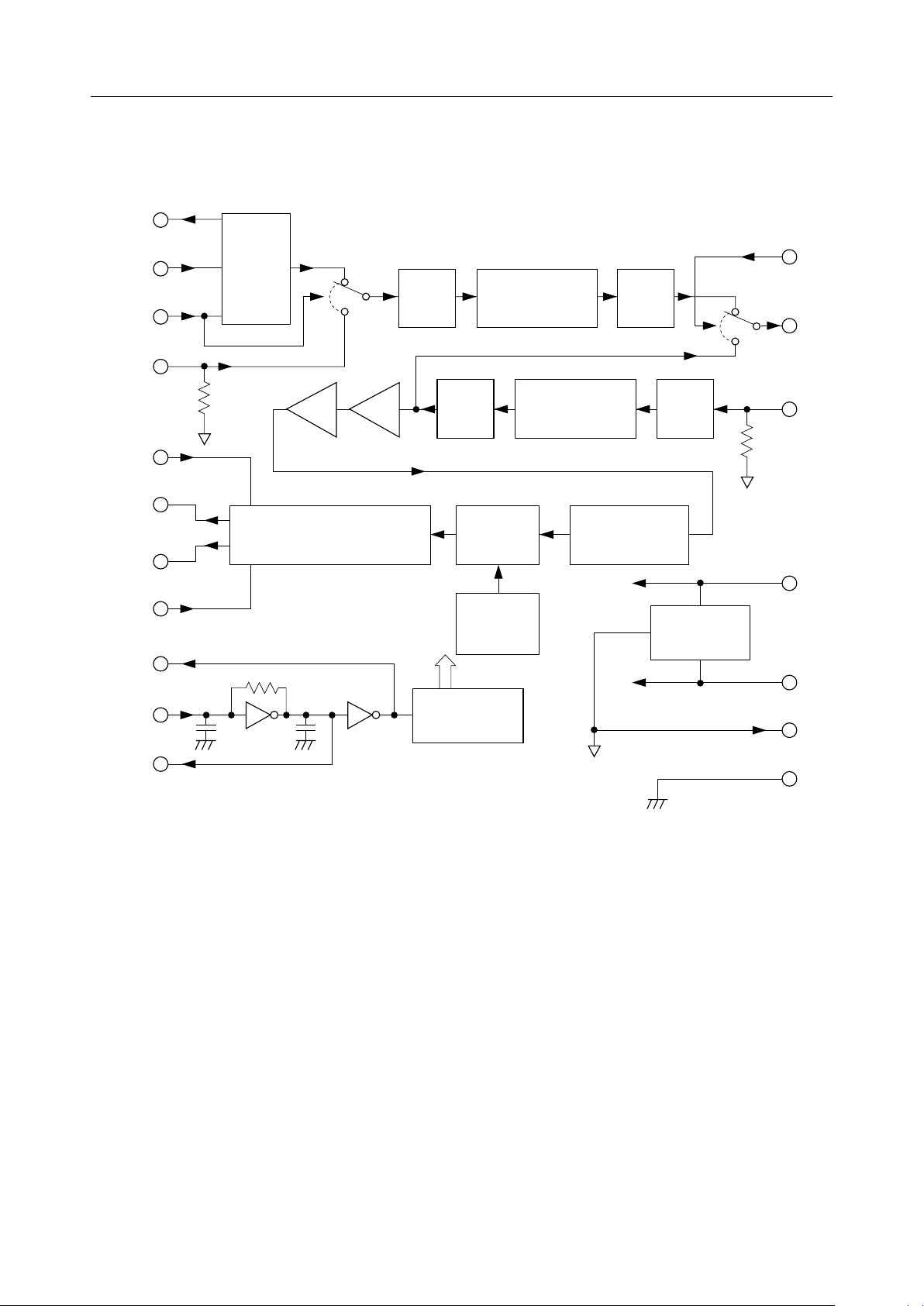
BLOCK DIAGRAM
ST
*2
SD
ME
TI
CF
RT
RD
CT
MCK
X1
Modulator
SH LIM
Timing
Re-generator
RC
LPF
Generator
RC
LPF
Clock
PDF
*1
Power
ON
Reset
Transmit
LPF
Receive
BPF
RC
LPF
Delay
Detector
RC
LPF
Signal
Ground
FT
AO
AI
V
AG
SG
DD
X2
*1 Post Detection Filter
*2 NC (MSM6948V)
DG
2/13

¡ Semiconductor MSM6948/6948V
PIN CONFIGURATION (TOP VIEW)
1
X1
2 17X2 FT
3
4
5
6
7
8
9
DG
18
V
16*MCK CT
15ME CF
14SD RT
13ST RD
12SG AI
11AG AO
10
TI
DD
X1
X2
*MCK
ME
(NC)
SD
(NC)
(NC)
ST
1
2
3
4
5
6
7
8
9
10 15SG AI
11
12
24
V
23
FT
22
CT
21
CF
20
(NC)
19
RT
18
(NC)
17
(NC)
16
RD
14AG AO
13DG TI
DD
18-Pin Plastic DIP
*NC (MSM6948V)
NC : No connect pin
24-Pin Plastic SOP
3/13

¡ Semiconductor MSM6948/6948V
PIN DESCRIPTION
Name Description
X1
X2
Crystal connection pins.
A 3.6864 MHz crystal shall be connected.
When an external clock is applied for MSM6948's oscillation source, it has to be input to X2.
In this case, X2 has to be AC-coupled by the capacitor of 200 pF. X1 shall be left open.
*MCK
ME
SD
ST
SG
3.6864 MHz ±0.02% clock output.
This can be used for other devices under limited load conditions.
When digital "1" is put on this pin, MSK modulator output is connected to the input of
transmit LPF.
When digital "0" is put on, the input of transmit LPF is connected to TI that is voice signal input.
The data put on ME terminal is synchronized with the rising edge of ST and input to internal
logic as a control data. The rising edge of this synchronized data resets MSK modulator.
Transmit data input.
The data on this pin is synchronized with the rising edge of ST and input to MSK modulator
as an actual transmit data.
SD
50%SD
ST
50%SD
MSK
Modulated
Data
t
setup
t
; Min. 300 ns
setup
; Min. 300 ns
t
hold
t
hold
ST is synchronizing signal used for ME and SD.
This is made from master clock and is usually 1200 Hz.
Built-in analog signal ground.
The DC voltage is approximately half of V
, so the analog signals of AI, AO, and TI interfaces
DD
with peripheral circuits which must be implemented by AC-coupling. To make this voltage
source impedance lower and ensure the device performance, it is necessary to put a bypass
capacitor on SG in close physical proximity to the device.
AG
*NC : MSM6948V
Analog ground.
This pin should be common with DG at the system ground point as close as possible.
4/13
 Loading...