
¡ Semiconductor MSM5718B70
1
¡ Semiconductor
MSM5718B70
18-Megabit RDRAM (2M ¥ 9)
DESCRIPTION
The 18-Megabit Rambus™ DRAM (RDRAM™) is an extremely high-speed CMOS DRAM organized
as 2M words by 9 bits. It is capable of bursting up to 256 bytes of data at less than 2 nanoseconds per
byte. The use of Rambus Signaling Logic (RSL) technology makes transfer rates greater than 500
MHz achievable while using conventional system and board design methodologies. Lower effective
latency is attained by operating the dual 2KByte sense amplifiers as high speed caches, and by using
random access mode to facilitate large block transfers.
RDRAMs are general purpose high-performance memory devices suitable for use in a broad range
of applications including PC and consumer main memory, graphics, video, and any other
application where high-performance is required.
FEATURES
• Rambus Interface:
Over 500 MB/sec peak transfer rate per RDRAM
Rambus Signaling Logic (RSL) interface
Synchronous protocol for fast block-oriented transfers
Direct connection to Rambus ASICs, MPUs, and Peripherals
15 active signals require just 32 total pins on the controller interface (including power)
3.3 V operation
Additional/multiple Rambus Channels provide an additional 500 MB/second band-width each
• Dual 2KByte sense amplifiers may be operated as caches for low latency access
• Random Access mode enables any burst order at full band width
• Features for graphics include random-access mode, write-per-bit and mask-per-bit operations
• Control and refresh logic entirely self-contained
• On-chip registers for flexible addressing and timing
• Available in horizontal surface mount plastic package (SHP32-P-1125-0.65-K)
E2G1033-17-54
MSM5718B70 ¡ Semiconductor
2
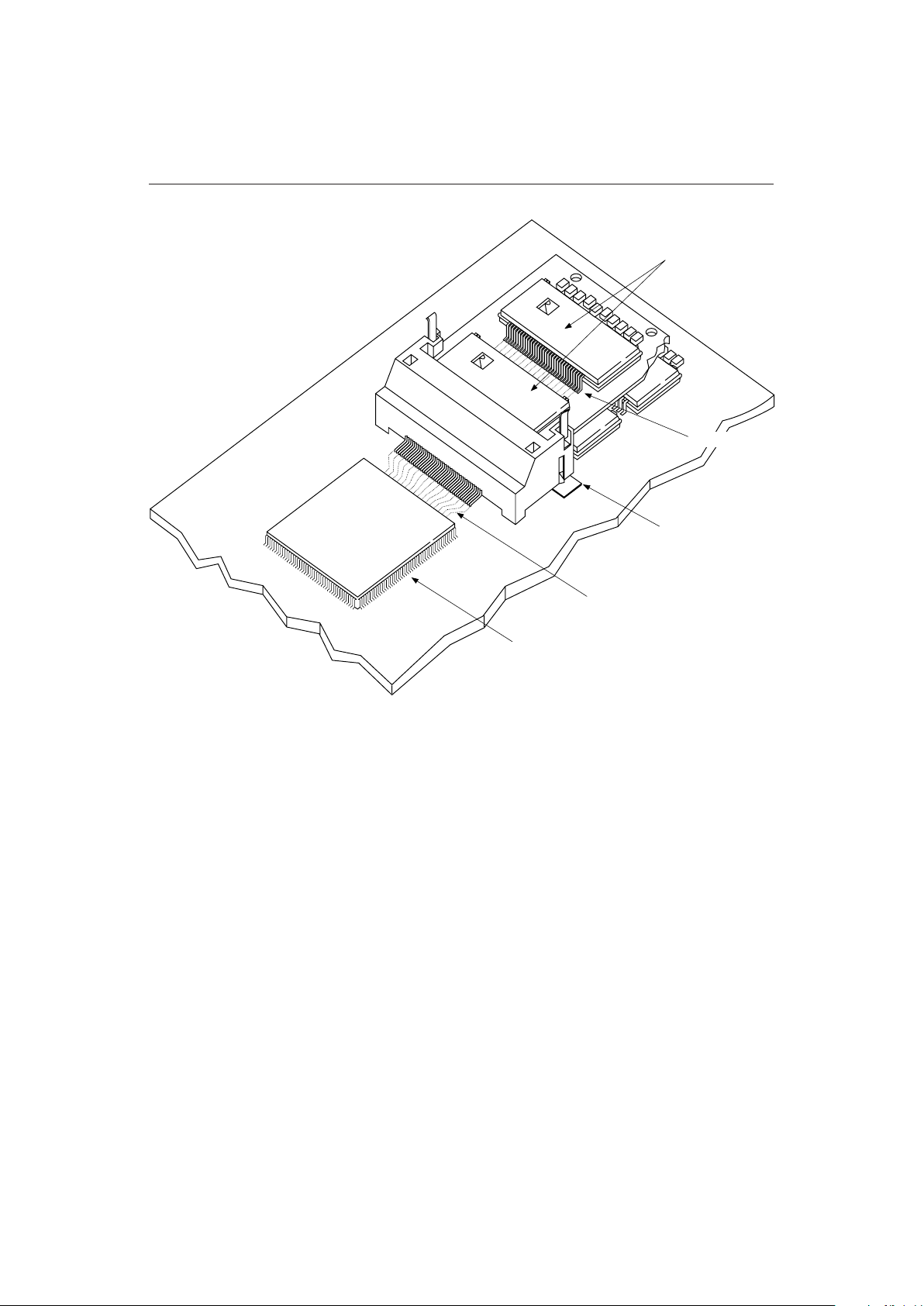
RDRAMs
RModule
RSocket
Rambus Channel
Controller
Fig. 1 Rambus Subsystem
SYSTEM BENEFITS
• Fully engineered solution includes clock chips, memory expansion sockets and simple layout
• For graphics subsystems addressing display resolutions of 1024 ¥ 768 ¥ 8 or above, it provides high
performance, fewest controller pins, and ease of memory expansion
• For Pentium® processor class main memory, it provides fast memory subsystem, fewer components,
and 2 MB granularity
• Sufficient performance for unified memory system architectures in consumer applications
PART NUMBERS
The 18-Megabit RDRAMs are available in horizontal surface mount plastic package (SHP), with a
500 MHz clock rate, a 533 MHz clock rate and a 600 MHz clock rate. The part numbers for the various
options are shown in Table 1.
¡ Semiconductor MSM5718B70
3
Table 1 Part Numbers
500 MHz 533 MHz
MSM5718B70-50GS-K MSM5718B70-53GS-K
600 MHz
MSM5718B70-60GS-K
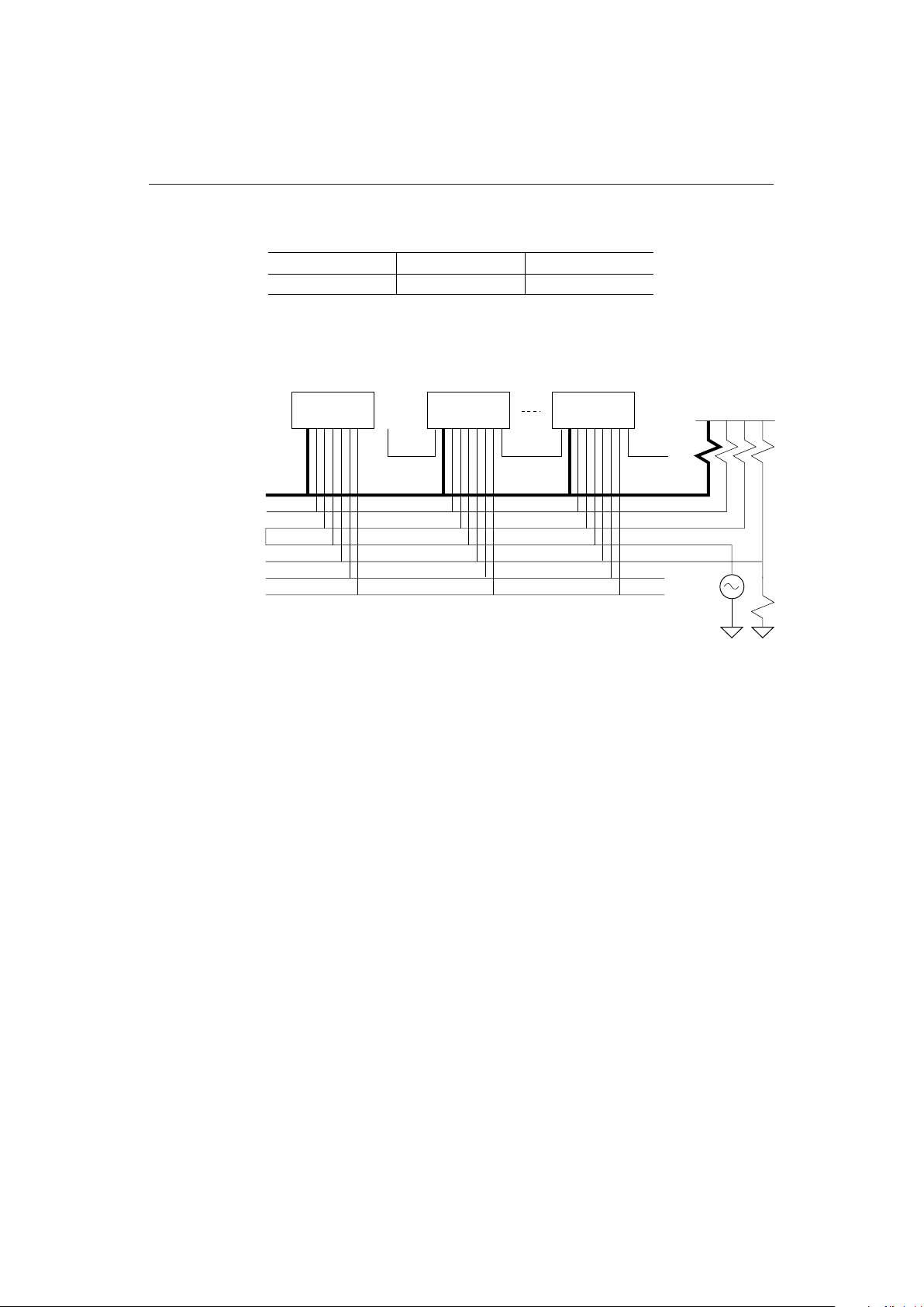
Fig. 2 Controller and RDRAMs Connect to Terminated Transmission Lines
RAMBUS SYSTEM OVERVIEW
A typical Rambus memory system has three main elements: the Rambus Controller, the channel, and
the RDRAMs. The logical representation of this is shown in Fig. 2.
The Rambus channel is a high-speed, byte-wide, synchronous bus used to connect Rambus devices
together. The channel carries all address, data, and control information to and from devices. Transfer
of data on the Rambus channel is managed through the use of a high level block-oriented protocol.
BusData [8:0]
BusCtrl, BusEnable
ClkFromMaster
ClkToMaster
Vref
Gnd, GndA
Vdd, VddA
Controller RDRAM 1 RDRAM n
V
term
SIn
Rambus Channel = 9 bits every 2 ns
Vdd
SOut
NC
SInSOut
MSM5718B70 ¡ Semiconductor
4
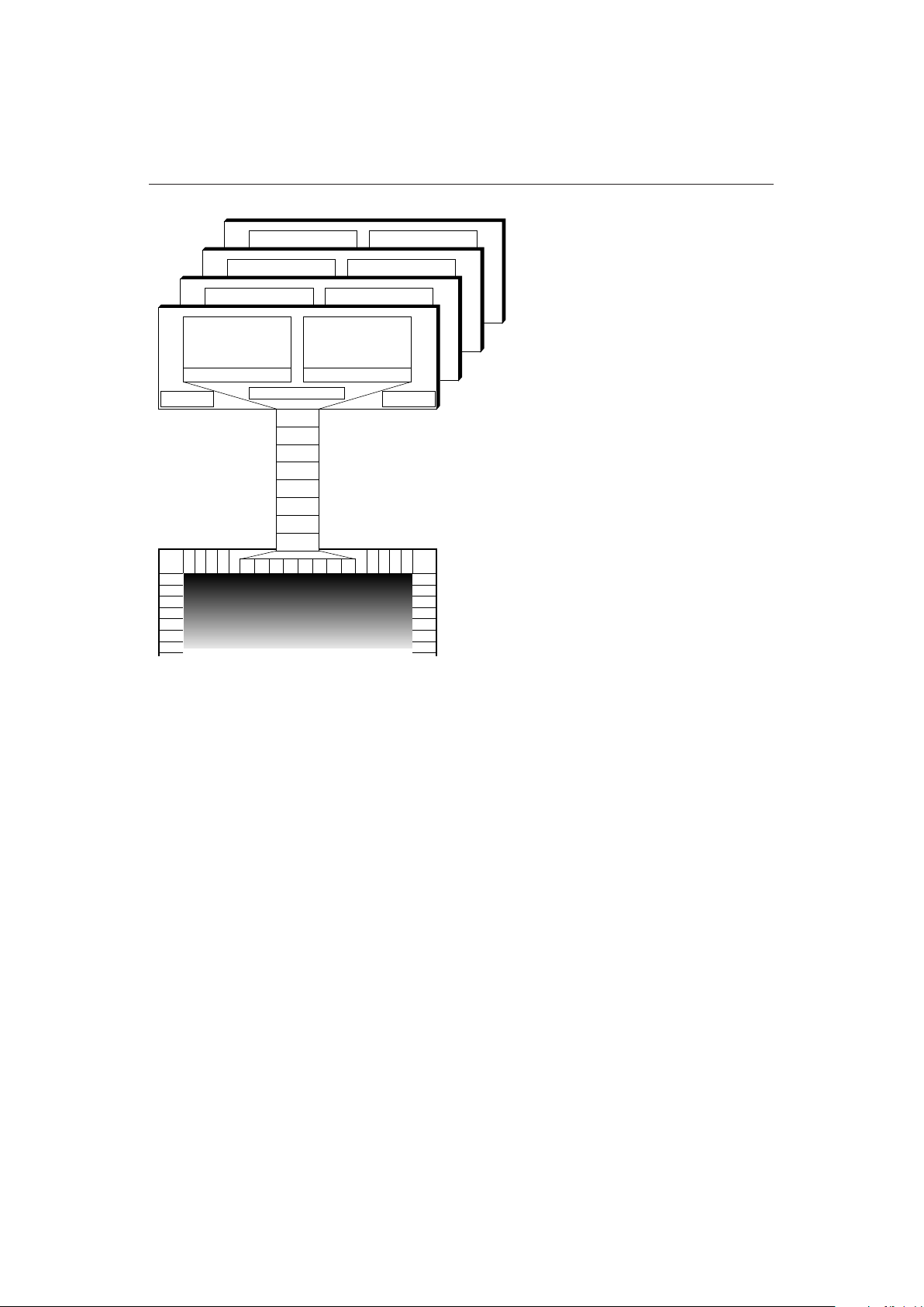
a b c d e f g h
Byte h
Byte g
Byte f
Byte e
Byte d
Byte c
Byte b
Bank 1 Bank 2
Sense Amp Cache page 1 Sense Amp Cache page 2
Address Comparators
Registers
Bank 3 Bank 4
Bank 5 Bank 6
Bank 7 Bank 8
RDRAM 4
RDRAM 3
RDRAM 2
RDRAM 1
Clocking
Rambus Channel
9 bits every 2 ns
Rambus Interface Cell
Macrocell in embedded array and standard cell libraries
Converts Rambus channel small swing signals to ASICcore-compatible CMOS levels
Converts 9 bits every 2 ns to 72 bits (X2) every 16 ns
Contains PLLs
•
•
•
•
Byte a
The Rambus channel has thirteen high-speed Rambus Signaling Logic (RSL) I/O signals that are
used to transfer information at 2 nanosecond intervals. These signals use low voltage swings (logic
0 = 2.25 V, logic 1 = 1.55 V) to achieve high bus speeds. Two TTL level signals are used for initialization
and powerdown operation. Fourteen signals supply power and DC voltage references to the
RDRAM, and the remaining pins are No Connects (reserved for future expansion).
The Rambus interface is implemented on both master and slave devices. Rambus masters (ASIC
devices, memory controllers, graphics engines, peripheral chips, or microprocessors) are the only
devices capable of generating transaction requests. RDRAMs are slave devices and can respond to
requests from master devices.
Fig. 1 shows a typical physical implementation of a Rambus system. It includes a controller ASIC
that acts as the Channel master and a base set of RDRAMs soldered directly to the board. An
RSocket™ is included on the Channel for memory upgrade using RModule™ expansion cards.
Fig. 3 Data Transfer on the Rambus Channel

¡ Semiconductor MSM5718B70
5
RDRAM PACKAGES AND PINOUTS
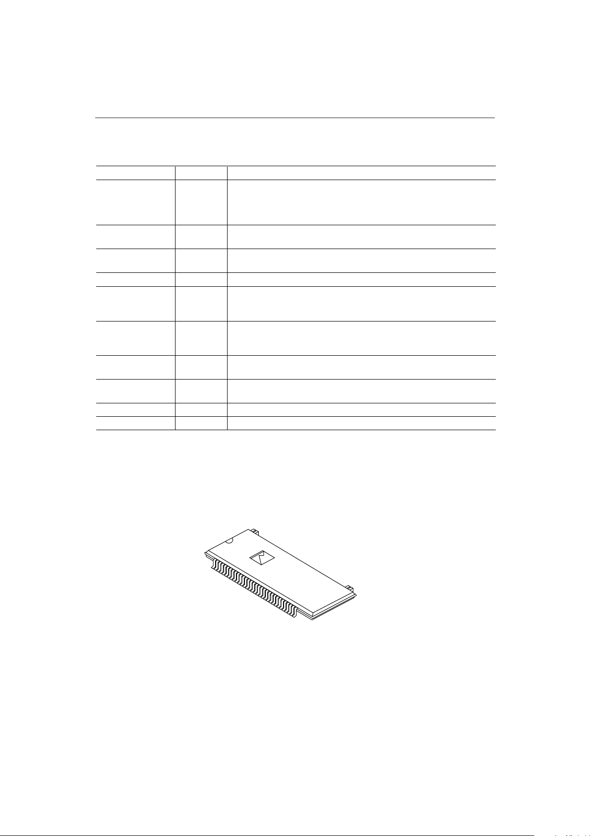
RDRAMs are available in horizontal surface mount plastic package (SHP).
The package has 32 signal pins and four mechanical pins that provide support for the device. The
mechanical pins are located on the opposite side from the signal leads in the SHP.
V
DD
1
Gnd
2
BusData8 3
Gnd 4
BusData7
5
(NC) 6
BusEnable
7
V
DD
8
BusData6 9
Gnd
10
BusData5 11
V
DDA
12
RxClk 13
GndA 14
TxClk
15
V
DD
16
BusData4
17
Gnd 18
BusCtrl 19
SIn
20
V
REF
21
SOut
22
BusData3 23
Gnd 24
BusData2
25
(NC) 26
BusData1 27
Gnd
28
BusData0 29
(NC)
30
Gnd 31
V
DD
32
Fig. 4 SHP Pin Numbering
MSM5718B70 ¡ Semiconductor
6
Table 2 Pin Descriptions
Signal lines for request, write data, and read data packets. The request
packet contains the address, operation codes, and the count of the bytes
to be transferred. These are low-swing active-low signals referenced to
Vref.
Signal I/O Description
BusData [8-0] I/O
Receive clock. Incoming request and write data packets are aligned to
this clock. This is a low-swing active-low signal referenced to Vref.
RxClk I
Transmit clock. Outgoing acknowledge and read data packets are aligned
with this clock. This is a low-swing active-low signal referenced to Vref.
TxClk I
Logic threshold reference voltage for low swing signals.
Vref I
Control signal to frame packets transmit part of the operation code to
acknowledge requests, and to interrupt (terminate) pending transactions.
This is a low-swing active-low signal referenced to Vref.
BusCtrl I/O
Control signal to manage the operating modes of the RDRAMs and to
transfer column addresses for random-access (non-sequential) transactions.
This is a low-swing active-low signal referenced to Vref.
BusEnable I
+3.3V power supply. VddA is a separate analog supply for clock recovery
in the RDRAM.
Vdd, VddA
Circuit ground. GndA is a separate analog ground for clock generation in
the RDRAM.
Gnd, GndA
Initialization daisy chain input. TTL levels. Active high.
SIn I
Initialization daisy chain output. TTL levels. Active high.
SOut O
Pin 1
Pin 32
Mechanical
Pins
Mechanical
Pins
Fig. 5 SHP Package
¡ Semiconductor MSM5718B70
7
PROTOCOL
The transaction protocol used in Rambus systems is built from several types of information packets.
These include the request, acknowledge, serial mode, and data packets.
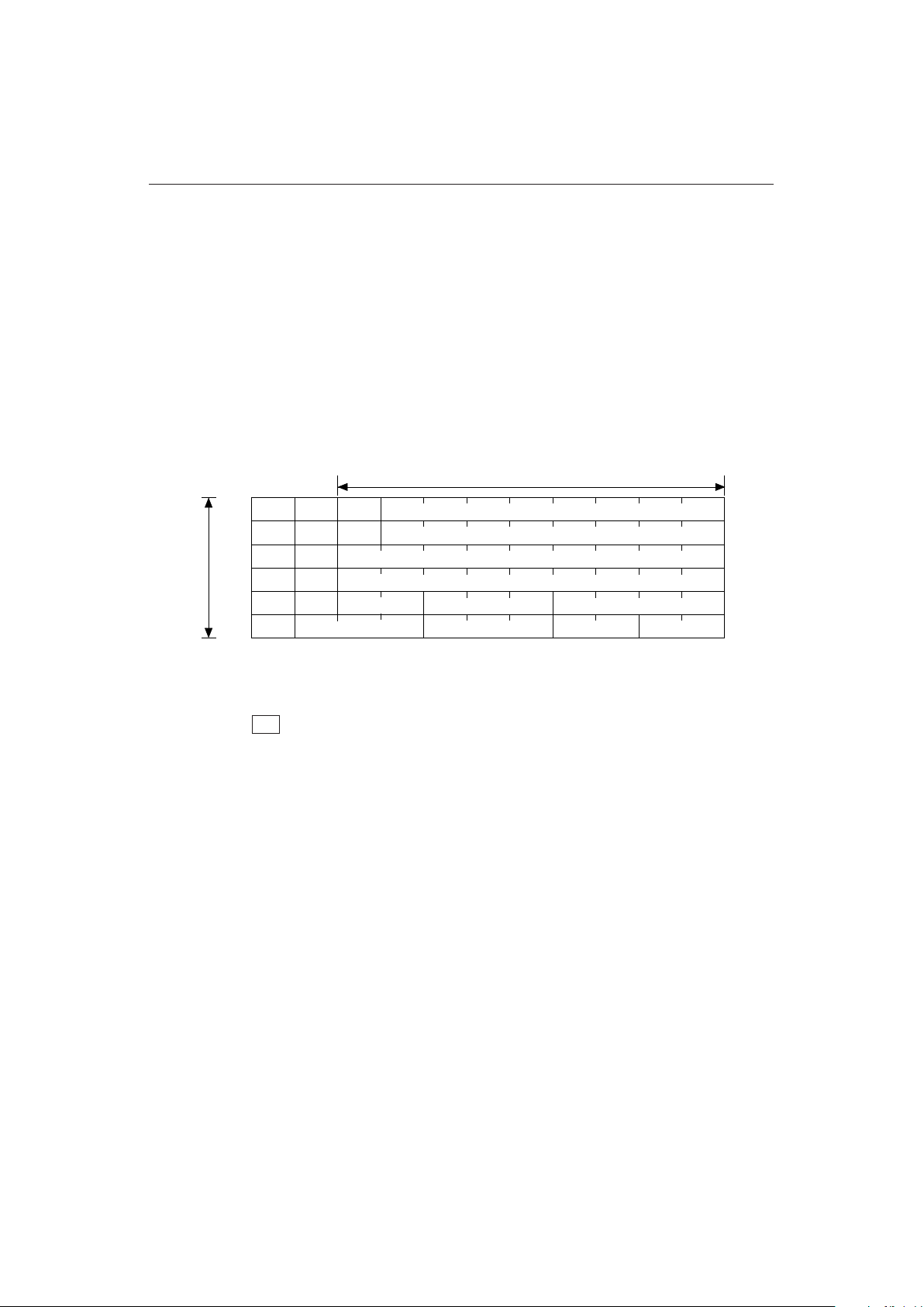
Request Packet
A master device initiates a transaction by generating a six-byte request packet containing address,
control, and byte count information as shown in Fig. 6. The Op and OpX fields in the Request packet
contain a command that is used to instruct the RDRAM which operation is being requested. A
summary of these commands is shown in Table 3.
Start Op[0]
Bus-
Ctrl
Bus-
Enable
BusData (8:0)
Adr[9:2]
Op[1] Op[3] Adr[17:10]
OpX[1] Adr[26:18]
Op[2] Adr[35:27]
OpX[0] Count[6, 4, 2]ReqUnimp[5:4] ReqUnimp[3:0]
Count[7, 5, 3]ReqUnimp[8:6] Count[1:0] Adr[1:0]
—
—
—
—
—
—
[0]
even
[0]
odd
[1]
even
[1]
odd
[2]
even
[2]
odd
Time
Clock Cycle Number
Fig. 6 Request Packet
1
Note: 1. A — in this diagram signifies that this pin is not used by this packet. If it is not used
by another packet, it is pulled to a logic zero value.

MSM5718B70 ¡ Semiconductor
8
Table 3 Command Summary
Op[3:0] OpX[1:0] Name Description
Read sequential data from memory space.
0000 00 Rseq
Read random-access (non-sequential) data from memory space.0000 01 Rnsq
Write sequential data to memory space with no per-bit mask application.0100 00 WseqNpb
Write sequential data to memory space with data-per-bit masking. Static
bit masks are supplied by the MDReg while write data is supplied in the
data packet.
0100 01 WseqDpb
Write sequential data to memory space with mask-per-bit masking. Both
write data and dynamic bit masks are supplied in the data packet.
0100 10 WseqBpb
Write sequential data to memory space with mask-per-bit masking. Static
write data is supplied by the MDReg while dynamic bit masks are supplied
in the data packet.
0100 11 WseqMpb
Read data from register space.
0110 00 Rreg
Write data to register space.
0111 00 Wreg
Write random-access (non-sequential) data to memory space with no perbit mask application.
1000 00 WnsqNpb
Write random-access (non-sequential) data to memory space with maskper-bit masking. Both write data and dynamic bit masks are supplied in
the data packet.
1000 10 WnsqBpb
Write random-access (non-sequential) data to memory space with maskper-bit masking. Static write data is supplied by the MDReg while dynamic
bit masks are supplied in the data packet.
1000 11 WnsqMpb
Write random-access (non-sequential) data to memory space with byte
masking and no per-bit mask application. Both byte masks and write data
are supplied in the data packet.
1100 00 WbnsNpb
Write random-access (non-sequential) data to memory space with byte
masking and data-per-bit masking. Static bit masks are supplied by the
MDReg while byte masks and write data are supplied in the data packets.
1100 01 WbnsDpb
Write random-access (non-sequential) data to memory space with byte
masking and mask-per-bit masking. Static write data is supplied by the
MDReg while byte masks and dynamic bit masks are supplied in the data
packets.
1100 11 WbnsMpb
Broadcast write to register space of all responding devices with no acknowledge permitted.
1111 WregB00
Write random-access (non-sequential) data to memory space with data-perbit masking. Static bit masks are supplied by the MDReg while write data is
supplied in the data packet.
01 WnsqDpb
1000
¡ Semiconductor MSM5718B70
9
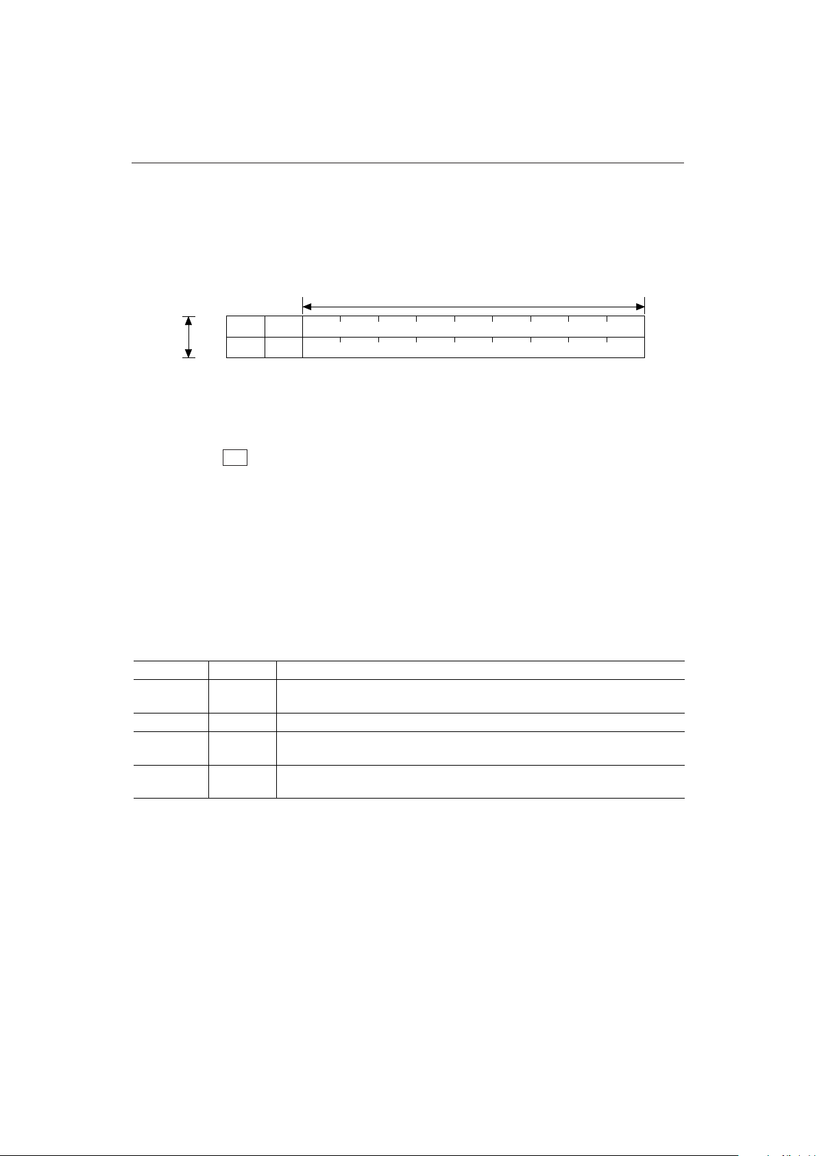
Acknowledge Packet
Each RDRAM monitors the channel for a request to access its assigned memory range. The device
matching the address range requested then drives an acknowledge packet back to the master.
Ack[0]
Bus-
Ctrl
Bus-
Enable
BusData (8:0)
Ack[1]
—
—
[0]
even
[0]
odd
Time
Clock Cycle Number
—
—
The Ack[1:0] field in the Acknowledge packet carries the RDRAM's response to the request. If the
RDRAM is able to complete the operation as requested, it returns an okay response. If the RDRAM
is unable to complete the operation as requested, it returns a negative acknowledge response (Nack).
The encoding of the Ack[1:0] bits is shown in Table 4.
Table 4 Ack[1:0] Encodings
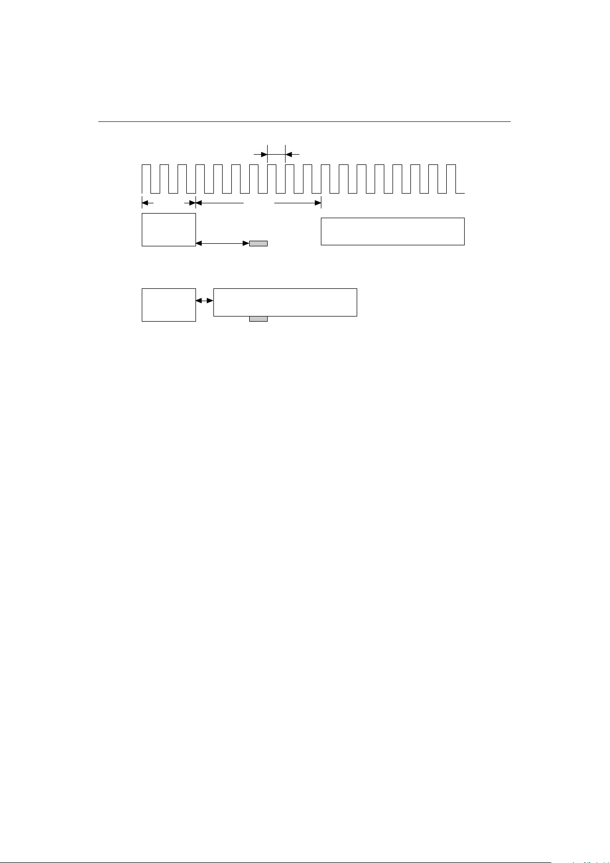
In response to an acknowledged command, the RDRAM either drives a data packet back to the
master in the case of a read, or accepts a data packet from the master in the case of a write. Fig. 8 shows
an example of 16 byte read and write transactions. The actual timing from the end of a request packet
to data and acknowledge packets is adjustable through RDRAM register settings.
Ack [1:0] Name Description
Indicates passive acceptance of the request (WregB), or indicates that the addressed
device did not respond (all other commands).
00
Non-
existent
Indicates that the request was accepted by the addressed (responding) device.
01 Okay
Indicates that the request could not be accepted because the state of the responding
device prevented an access at the fixed timing slot.
10 Nack
This should not be returned by this responding device. Initiating devices will, when
presented with this combination, have an undefined response.
11 Ack3
Fig. 7 Acknowledge Packet
1
Note: 1. A — in this diagram signifies that this pin is not used by this packet. If it is not used
by another packet, it is pulled to a logic zero value.
MSM5718B70 ¡ Semiconductor
10
1t
CYCLE
3t
CYCLE
7t
CYCLE
3t
CYCLE
Read Request Read DataAck
1t
CYCLE
Ack
Write Request Write Data
Fig. 8 Sample 16-Byte Read and Write Transactions
¡ Semiconductor MSM5718B70
11
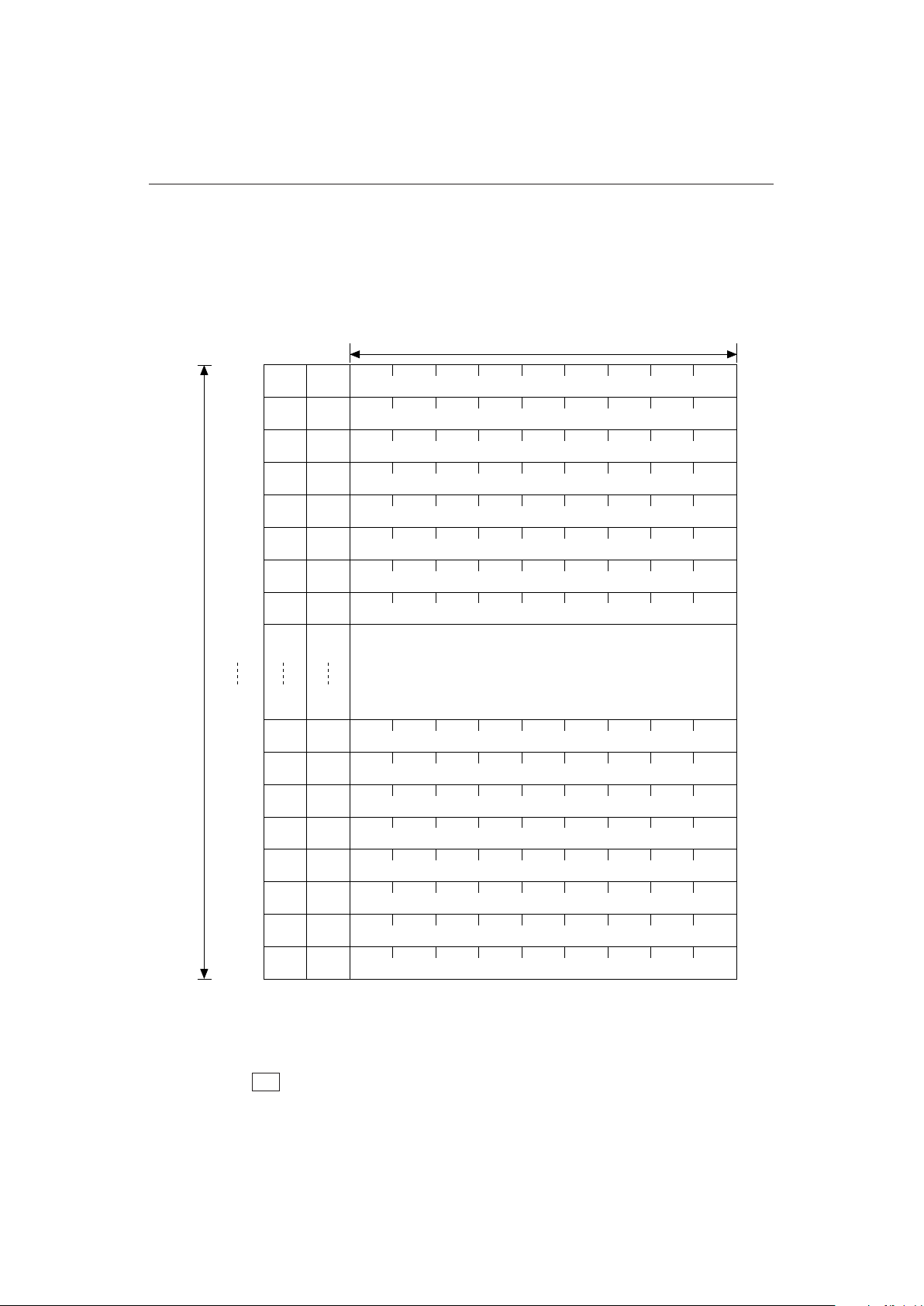
Serial Address Packet
The non-sequential (Random Access) commands specify the eight column address bits needed to
access random octbytes within the open page. These address bits are provided using a Serial Address
packet.
SAdr
[1][3]
Bus-
Ctrl
Bus-
Enable
BusData (8:0)
—
—
[4]
even
Clock Cycle Number
—
—
SAdr
[1][4]
[4]
odd
SAdr
[1][5]
—
—
[5]
even
—
—
SAdr
[1][6]
[5]
odd
SAdr
[1][7]
—
—
[6]
even
—
—
SAdr
[1][8]
[6]
odd
SAdr
[1][9]
—
—
[7]
even
—
—
SAdr
[1][10]
[7]
odd
SAdr
[n][3]
—
—
[4*n]
even
—
—
SAdr
[n][4]
[4*n]
odd
SAdr
[n][5]
—
—
[4*n+1]
even
—
—
SAdr
[n][6]
[4*n+1]
odd
SAdr
[n][7]
—
—
[4*n+2]
even
—
—
SAdr
[n][8]
[4*n+2]
odd
SAdr
[n][9]
—
—
[4*n+3]
even
—
—
SAdr
[n][10]
[4*n+3]
odd
Time
Fig. 9 Serial Address Packet Format
1
Note: 1. A — in this diagram signifies that this pin is not used by this packet. If it is not used
by another packet, it is pulled to a logic zero value.
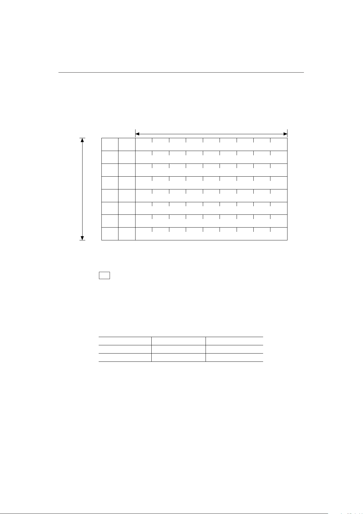
MSM5718B70 ¡ Semiconductor
12
Serial Control Packet
The protocol also allows the channel master to issue an early termination instruction for a memory
read or write transaction. This is done using a Serial Control packet.
SCtrl
[0]
Bus-
Ctrl
Bus-
Enable
BusData (8:0)
—
—
[0]
even
Clock Cycle Number
—
—
SCtrl
[1]
[0]
odd
SCtrl
[2]
—
—
[1]
even
—
—
SCtrl
[3]
[1]
odd
SCtrl
[4]
—
—
[2]
even
—
—
SCtrl
[5]
[2]
odd
SCtrl
[6]
—
—
[3]
even
—
—
SCtrl
[7]
[3]
odd
Time
The value of the Serial Control field specifies whether the instruction should continue or terminate.
This is shown in the table below.
Table 5 Serial Control Field
Serial Control Field Description Value
SCtrl[7:0] Continue 00000000
SCtrl[7:0] Terminate 00100000
Fig. 10 Serial Control Packet Format
1
Note: 1. A — in this diagram signifies that this pin is not used by this packet. If it is not used
by another packet, it is pulled to a logic zero value.
 Loading...