

OKI MSM5116400D-60TS-K, MSM5116400D-50TS-K, MSM5116400D-70SJ, MSM5116400D-60SJ, MSM5116400D-70TS-K Datasheet
...
Semiconductor
M SM5116400D
This version:Apr.1999
4,194,304-Word
4-Bit DYNA MIC RAM : FAST PAGE MODE TY PE
´´´´
DESCRIPTION
The MSM5116400D is a 4,194,304-word ´ 4-bit dynamic RAM fabricated in Oki’s silicon-gate CMOS
technology. The MSM5116400D achieves high integration, high-speed operation, and low-power consumption
because Oki manufactures the device in a quadruple-layer polysilicon/double-layer metal CMOS process. The
MSM5116400D is available in a 26/24-pin plastic SOJ, 26/24-pin plastic TSOP.
FEATURES
4,194,304-word ´ 4-bit configuration
·
Single 5V power supply, ±10% tolerance
·
Input : TTL compatible, low input capacitance
·
· Output : TTL compatible, 3-state
· Refresh : 4096 cycles/64 ms
· Fast page mode, read modify write capability
CAS before RAS refresh, hidden refresh, RAS-only refresh capability
·
· Multi-bit test mode capability
· Package options:
26/24-pin 300mil plastic SOJ (SOJ26/24-P-300-1.27) (Product : MSM5116400D-xxSJ)
26/24-pin 300mil plastic TSOP (TSOPII26/24-P-300-1.27-K) (Product : MSM5116400D-xxTS-K)
xx : indicates speed rank.
PRODUCT FAMILY
Family
MSM5116400D-50 50ns 25ns 13ns 13ns 90ns 413mW
MSM5116400D-60 60ns 30ns 15ns 15ns 110ns 385mW
MSM5116400D-70 70ns 35ns 20ns 20ns 130ns 358mW
Access Time (Max.) Power Dissipation
t
RAC
t
AA
t
CAC
t
OEA
Cycle Time
(Min.)
Operating (Max.) Standby (Max.)
5.5mW
1/14
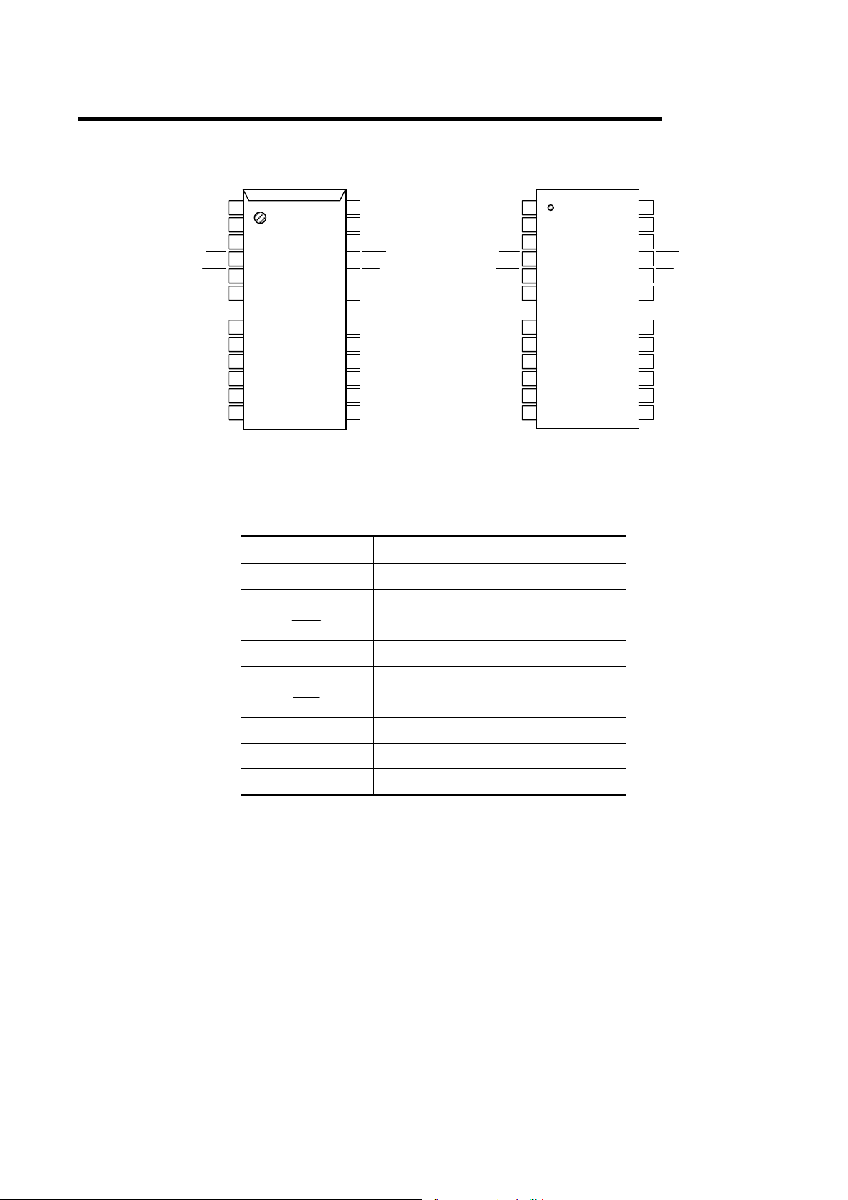
PIN CONFIGRATION (TOP VIEW)
MSM5116400D
V
1
CC
DQ1
2
DQ2
3
WE
4
RAS
5
A11
6
A10
8
9
A0
10
A1
11
A2
12
A3
13
V
CC
26/24-Pin Plastic SOJ
Pin Name Function
A0–A11 Address Input
V
DQ1
DQ2
WE
RAS
A11
A10
A0
A1
A2
A3
V
1
CC
2
3
4
5
6
8
9
10
11
12
13
CC
26
25
24
23
22
21
19
18
17
16
15
14
V
SS
DQ4
DQ3
CAS
OE
A9
A8
A7
A6
A5
A4
V
SS
26/24-Pin Plastic TSOP
RAS Row Address Strobe
(K Type)
26
25
24
23
22
21
19
18
17
16
15
14
V
SS
DQ4
DQ3
CAS
OE
A9
A8
A7
A6
A5
A4
V
SS
CAS Column Address Strobe
DQ1–DQ4 Data Input/Data Output
OE Output Enable
WE Write Enable
V
CC
V
SS
Power Supply (5V)
Ground (0V)
NC No Connection
2/14
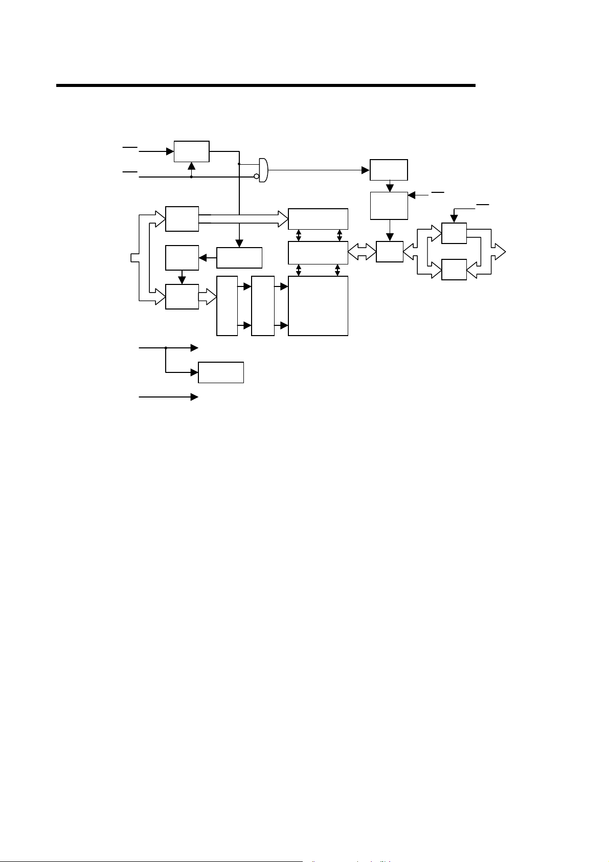
BLOCK DIAGRAM
A
DQ
DQ
OE
WE
RAS
CAS
VCCV
Column
10
Address
Buffers
Internal
0 – A11
Address
Counter
Address
Buffers
Timing
Generator
Row
1212
On Chip
V
Generator
BB
Refresh
Control Clock
Row
Deco-
ders
Word
Drivers
10
Column Decoders
Sense Amplifiers
Memory
Cells
Timing
Generator
Write
Clock
Generator
I/O
Selector
MSM5116400D
Output
4
Buffers
44
4
Buffers
Input
4
4
4
1 -
4
SS
3/14
ELECTRICAL CHARACTERISTICS
Absolute Maximum Ratings
Parameter Symbol Rating Unit
MSM5116400D
Voltage on Any Pin Relative to V
SS
Short Circuit Output Current
Power Dissipation
Operating Temperature
Storage Temperature
*: Ta = 25°C
Recommended Operating Conditions
Parameter Symbol Min. Typ. Max. Unit
V
Power Supply Voltage
Input High Voltage
Input Low Voltage
V
V
V
CC
SS
IH
IL
V
T
I
OS
P
D*
T
opr
T
stg
0.5 to 7.0
-
50 mA
1W
0 to 70 °C
55 to 150
-
V
°C
(Ta = 0°C to 70°C)
4.5 5.0 5.5 V
000V
*1
0.5
+
0.8 V
V
-
2.4
0.5
¾
*2
¾
V
CC
Notes: *1. The input voltage is VCC + 2.0V when the pulse width is less than 20ns (the pulse width is with
respect to the point at which V
*2. The input voltage is V
the point at which V
SS
- 2.0V when the pulse width is less than 20ns (the pulse width respect to
SS
is applied).
is applied).
CC
Capacitance
(VCC = 5.0V ± 10%, Ta = 25°C, f=1MHz)
Parameter Symbol Typ. Max. Unit
Input Capacitance (A0 – A11)
Input Capacitance
(RAS, CAS, WE, OE)
Output Capacitance (DQ1 – DQ4)
C
C
C
IN1
IN2
I/O
¾
¾
¾
5pF
7pF
7pF
4/14
DC Characteristics
MSM5116400D
(VCC = 5V ± 10%, Ta = 0°C to 70°C)
Parameter
Output High Voltage
Output Low Voltage
Input Leakage
Current
Output Leakage
Current
Average Power
Supply Current
(Operating)
Power Supply
Current
(Standby)
Average Power
Supply Current
(RAS-only Refresh)
Symbol
V
OH
V
OLIOL
I
LI
I
LO
I
CC1
I
CC2
I
CC3
Condition
IOH = -5.0mA
= 4.2mA
0V £ VI £ 6.5V ;
All other pins not
under test = 0V
DQ disable
0V £ V
O
£ V
CC
RAS, CAS cycling,
t
= Min.
RC
RAS, CAS = V
RAS, CAS
– 0.2V
V
CC
IH
³
RAS cycling,
CAS = V
t
RC
= Min.
IH
,
MSM5116400
D-50
Min.
Max
2.4 V
MSM5116400
Min.
2.4 V
CC
D-60
Max
CC
MSM5116400
D-70
Min.
2.4 V
Max
CC
Unit Note
V
00.400.400.4V
10
-
10
-
¾
¾
10
10
75
2
10
-
10
-
¾
¾
10
10
70
2
10
-
10
-
¾
¾
10
10
A
m
A
m
65 mA 1,2
2
mA 1
¾
¾
0.5
75
¾
¾
0.5
70
¾
¾
0.5
65 mA 1,2
I
CC5
RAS = VIH,
CAS = V
,
IL
DQ = enable
¾
2
Power Supply
Current
(Standby)
Average Power
Supply Current
(CAS before RAS
RAS = cycling,
I
CC6
CAS before RAS
¾
75
Refresh)
I
CC7
RAS = VIL,
CAS cycling,
t
= Min.
PC
¾
70
Average Power
Supply Current
(Fast Page Mode)
Notes: 1. ICC Max. is specified as ICC for output open condition.
2. The address can be changed once or less while RAS = V
3. The address can be changed once or less while CAS = V
¾
¾
¾
2
70
65
.
IL
.
IH
¾
¾
¾
2mA1
65 mA 1,2
60 mA 1,3
5/14
 Loading...