

OKI MSM13Q0150, MSM13Q0340, MSM14Q0230, MSM13Q0840, MSM13Q0530 Datasheet
...
D
ATA SHEET
OKI ASIC PRODUCTS
MSM13Q/14Q000
0.35 µm Sea of Gates Arrays
November 1999

■ ■
–––––––––––––––––––––––––––––––––––––––––––––––––––––––––––––––––––––––––––––––––––––––––––
Oki Semiconductor

MSM13Q0000/14Q0000
0.35 µm Sea of Gates Arrays
DESCRIPTION
Oki’s 0.3 5 µm ASIC products deliver ultra-high performance and high density at low power dissipation.
The MSM13Q0000/14Q0000 series devices (referred to as “MSM13Q/14Q”) are implemented with the
industry-standard Cell-Based Array (CBA) architecture in a Sea-of-Gates (SOG) structure. Built in a
0.35 µm drawn CMOS technology (with an L-Effective of 0.27 µm), these SOG devices are available in
three layers (MSM13Q) and four layers (MSM14Q) of metal. The semiconductor process is adapted from
Oki’s production-proven 64-Mbit DRAM manufacturing process.
The MSM13Q/14Q Series contains 6 arrays each, offering over 1 million raw gates and 352 I/O pads. Up
to 66% and 90% of the raw gates can be used for the 3-layer and 4-layer arrays, respectively. Oki’s 0.35
µm family is optimized for 3-V core operation with optimized 3-V I/O buffers and 5-V tolerant 3-V buffers. These SOG products are designed to fit the most popular plastic quad flat packs (QFPs), thin QFPs
(TQFPs) , and plastic ball grid array (PBGA) packages.
The MSM13Q/14Q Series uses the popular CBA architecture from Silicon Architects of Synopsys which
mixes two types of cells (8-transistor compute cells and 4-transistor drive cells) on the same die to deliver
high gate density and high drives. The CBA is supported by a rich macro library, optimized for synthesis.
Memory blocks are efficiently created by Oki’s memory compilers to generate single- and dual-port
RAM’s in high-density and low-power configurations with synchronous RAM options.
As such, the MSM13Q/14Q series is well suited to memory-intensive designs with high production volumes approaching the real estate and cost savings of standard cells. At the same time, its SOG architecture allows rapid prototyping turnaround times. Thus, Oki’s MSM13Q/14Q family offers the best of two
worlds: quick prototyping of a gate array and low production cost of a standard cell.
Oki’s 0.35 µm ASIC products are supported by leading-edge CAD tools including a synthesis-linked
floorplanner, motive static timing analyzer, and H-clock tree methodology. They are further supported
by specialized macrocells including phase-locked loop (PLL), pseudo-emitter coupled logic (PECL),
peripheral component interconnect (PCI), universal synchronous receiver/transmitter (UART) cells, and
ARM7TDMI RISC cores.
FEATURES
• 0.35 µm drawn 3- and 4-layer metal CMOS
• Optimized 3.3-V core
• Optimized 3-V I/O and 3-V I/O that is 5-V
tolerant
• CBA SOG architecture
• Over 1.0M raw gates and 352 pads
• User-configurable I/O with V
state, and 1- to 24-mA options
• Slew-rate-controlled outputs for low-radiated
noise
• H-clock tree cells which reduce the maximum
skew for clock signals
, VDD, TTL, 3-
SS
• User-configurable single and dual-port;
synchronous or asynchronous memories
• Specialized macrocells including PLL, PECL,
PCI, UART, and ARM7TDMI
• Floorplanning for front-end simulation, backend layout controls, and link to synthesis
• Joint Test Action Group (JTAG) boundary scan
and scan-path ATPG
• Support for popular CAE systems, including
Cadence, IKOS, Mentor Graphics, Synopsys,
Viewlogic, and Zycad
1Oki Semiconductor
■
MSM13Q0000/14Q0000 ■ ––––––––––––––––––––––––––––––––––––––––––––––––––––––––––––––––––––––––
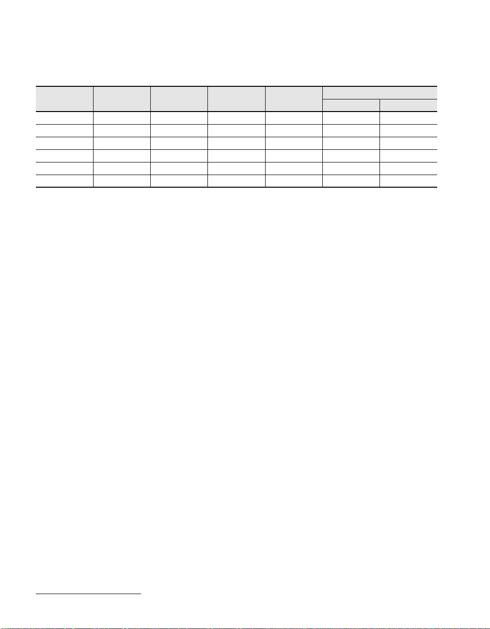
MSM13Q/14Q FAMILY LISTING
MSM13Q/14Q
Series
0150 144 157,192 105,319 143,045 196 802
0230 176 242,400 152,712 208,464 240 1,010
0340 208 346,176 204,244 276,941 288 1,202
0530 256 536,400 289,656 391,572 360 1,490
0840 320 847,048 415,054 567,522 452 1,874
1020 352 1,033,000 475,180 650,790 500 2,066
PAD No.
Raw Gate
(Gates)
Usable Gate
M13Q(3LM)
Usable Gate
M14Q(4LM)
Raw Gate
Row Column
ARRAY ARCHITECTURE
The primary components of a 0.35 µm MSM13Q/14Q circuit include:
• I/O base cells
• Configurable I/O pads for VDD, VSS, or I/O (optimized 3-V I/O and 3-V I/O that is 5-V tolerant)
•V
and VSS pads dedicated to wafer probing
DD
• Separate power bus for output buffers
• Separate power bus for internal core logic and input buffers
• Core base modules containing three compute cells for each drive cell
• Isolated gate structure for reduced input capacitance and increased routing flexibility
Each array has 24 dedicated corner pads for power and ground use during wafer probing, with 4 pads
per corner. The arrays also have separate power rings for the internal core functions (V
and output drive transistors (V
DDO
and V
SSO
).
The array architecture uses optimally sized transistors to efficiently implement logic and memory in a
metal programmable technology. CBA uses two types of cells: compute cells and drive cells. The compute cell employs four PMOS and four NMOS trasnsistors whose sizes are optimized for logic and memory implementations as shown in
Figure 1
. The quantity and size of the transistors in a compute cell are
carefully selected to maximize the efficiency of most commonly used functions in VLSI design. The drive
cell consists of two large PMOS pull-up transistors and two large pull-down transistors. The compute
and drive cells are tiled to create a channelless core array, with three comput cells for each drive cell as
shown in
Figure 2
. The 3:1 ratio of compute to drive cells was selected for optimal implementation of
emerging applications. Macrocells are created using either compute cells, drive cells, or combinations of
compute and drive cells.
DDC
and V
SSC
)
2 Oki Semiconductor

––––––––––––––––––––––––––––––––––––––––––––––––––––––––––––––––––––––– ■ MSM13Q0000/14Q0000
Compute Cell Compute Cell Compute Cell Drive Cell
Figure 1. Base Cell Consisting of Three Compute Cells and One Drive Cell
■
Compute Cell Drive Cell
Figure 2. Core Array with Base Cell Mirrored Horizontally and Ver tically
3Oki Semiconductor

■
MSM13Q0000/14Q0000 ■ ––––––––––––––––––––––––––––––––––––––––––––––––––––––––––––––––––––––––
ELECTRICAL CHARACTERISTICS
Absolute Maximum Ratings (VSS = 0 V, Tj = 25°C)
Parameter
Power supply voltage V
Input voltage Normal buffers V
5-V tolerant V
Output voltage Normal buffers V
5-V tolerant V
Input current Normal buffers I
5-V tolerant I
Output current per I/O Normal buffers IO I
5-V tolerant I
Storage temperature T
Symbol Conditions Rated Value Unit
DD
O
O
I
I
O
stg
[1]
-0.3 to +4.6 V
I
I
-0.3 to VDD+0.3
-0.3 to 6.0
-0.3 to VDD+0.3
-0.3 to 6.0
-10 to +10
-6 to +6
= 1, 2, 4, 6, 8, 12, 24 mA -24 to +24
O
I
= 2, 4, 6, 8, 12 mA -8 to +8
O
– -65 to +150 °C
V
V
mA
mA
1. Permanent device damage may occur if ABSOLUTE MAXIMUM RATINGS are exceeded. Functional operation should be restricted to the conditions
in the other specifications of this data sheet. Exposure to absolute maximum rating conditions for extended periods may affect device reliability.
Recommended Operating Conditions (VSS = 0 V)
Parameter
Power supply voltage V
Junction temperature T
Symbol Rated Value Unit
(3 V) +3.0 to +3.6 V
DD
j
-40 to +85 °C
4 Oki Semiconductor
 Loading...