

OKI MSC1951-01GS-K, MSC1951-01RS Datasheet

E2C0027-27-Y2
¡ Semiconductor MSC1951-01
¡ Semiconductor
This version: Nov. 1997
Previous version: Jul. 1996
MSC1951-01
7-Segment ¥ 16-Digit or 16-Segment ¥ 6-Bargraph display Controller/Driver
GENERAL DESCRIPTION
MSC1951-01 is a Bi-CMOS bargraph and alphanumeric display controller designed to interface
with either vacuum fluorescent display.
MSC1951-01 can drive displays with up to 16 figures with either 16 segment bargraph or sevensegment type code plus a decimal point and comma tail.
MSC1951-01 adopts a serial interface system, which allows data transfer from the microcomputer
only by two signal lines of SCLK and DATA.
FEATURES
• Can display up to 16 digits of 7-segment type character with comma/point or of 16-segment
type bargraph.
• The number of display digits is programmable within 16.
• The brightness adjustment is programmable by 1/32 step.
• The display contents can be changed at any digit.
• Buit-in PLA can display alphanumeric characters, e.g., 0 to 9 A, C, E, F, P, L (capital letters), b,
and d (small letters). In addition, 16-segment dot display and bar display are allowed.
• Instruction is executed by one byte.
• Driver output
Current : –20 mA max. (Digit)
–10 mA (Segment), Plastic DIP
–05 mA (Segment), Plastic QFP
Withstand voltage : 58 V max.
• Can be used for LED.
• Pin compatible with 10951 manufactured by Rockwell.
• Power supply voltage : 5V ± 10%
• Package options:
40-pin plastic DIP (DIP40-P-600-2.54) (Product name : MSC1951-01RS)
44-pin plastic QFP (QFP44-P-910-0.80-K) (Product name : MSC1951-01GS-K)
1/17
¡ Semiconductor MSC1951-01
2/17
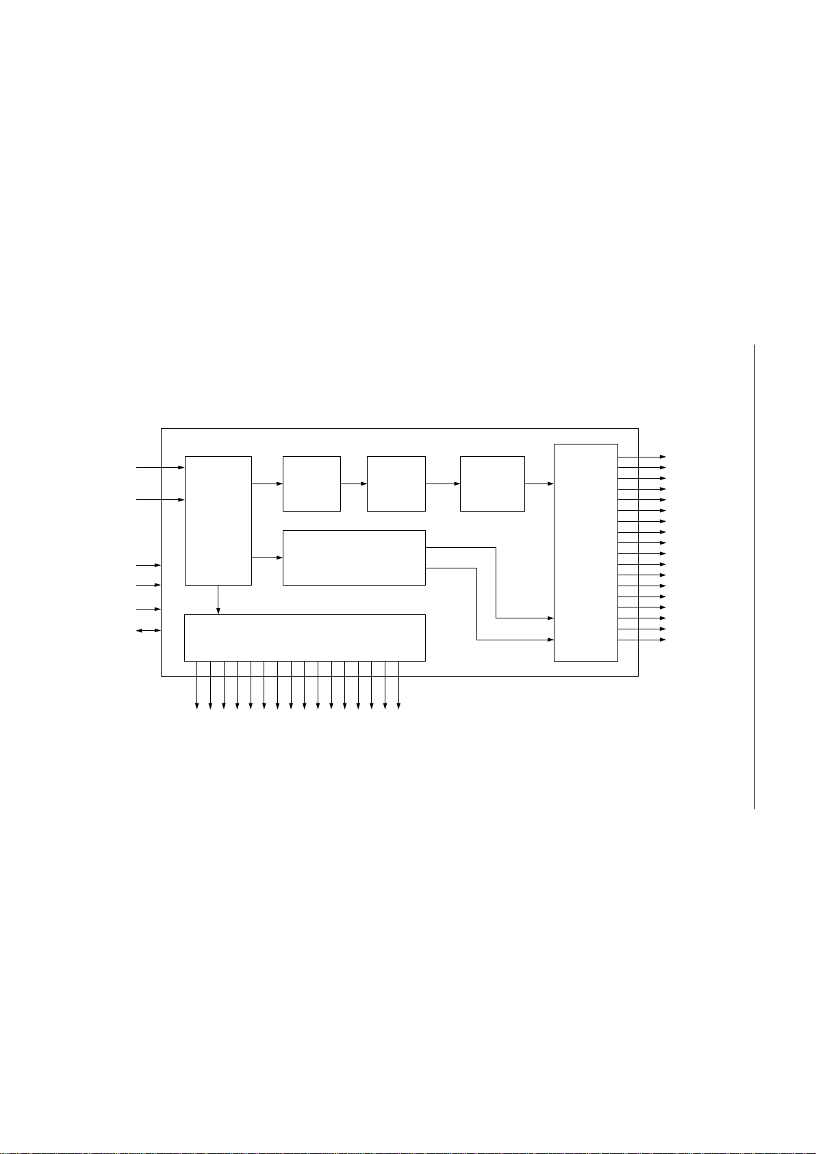
BLOCK DIAGRAM
SGA
SGB
SGC
SGD
SGE
SGF
SGG
SGH
SGI
SGJ
SGK
SGL
SGM
SGN
SGO
SGP
PNT
TAIL
AD16
AD15
AD14
AD13
AD12
AD11
AD10
AD 9
AD 8
AD 7
AD 6
AD 5
AD 4
AD 3
AD 2
AD 1
DATA
SCLK
POR
V
SS
V
DD
A
SEGMENT
DRIVERS
(ANODE)
SEGMENT
DECODER
64¥16
PLA
6¥16
DISPLAY
DATA
BUFFER
TIMING
AND
CONTROL
2¥16
DECIMAL PT.
COMMA TAIL
DIGIT DRIVERS
(GRID)

¡ Semiconductor MSC1951-01
INPUT AND OUTPUT CONFIGURATION
• Schematic Diagrams of Logic Portion Input Circuit
V
SS
V
SS
INPUT
V
DD
• Schematic Diagrams of Logic Portion Output Circuit
V
SS
V
SS
V
DD
OUTPUT
V
DD
• Schematic Diagrams of Driver Output Circuit
V
SS
V
SS
V
DD
OUTPUT
3/17
¡ Semiconductor MSC1951-01
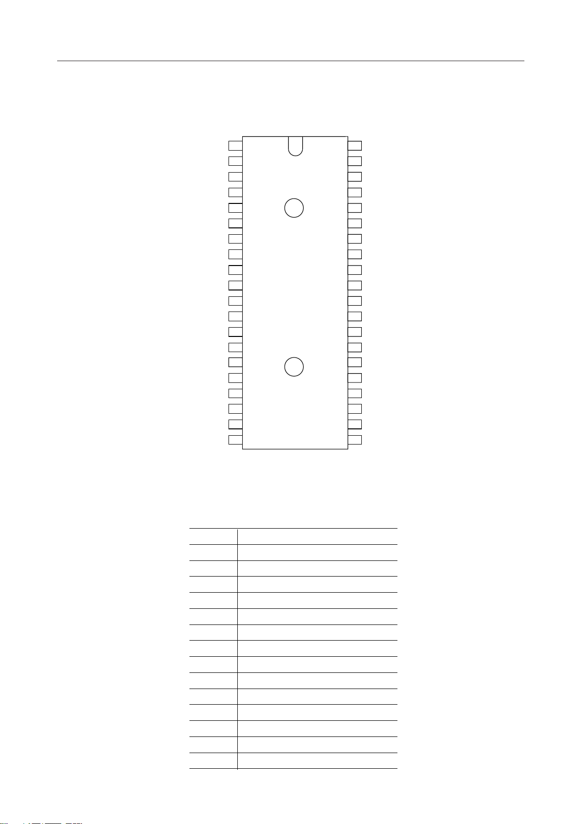
PIN CONFIGURATION (TOP VIEW)
V
DD
V
SS
AD16
AD15
AD14
AD13
AD12
AD11
AD10
AD 9
AD 8
AD 7
AD 6
AD 5
AD 4
AD 3
AD 2
AD 1
(GND)
POR
38
37
34
PNT
TAIL
SGP
SGO
SGN
SGM
SGL
SGK
SGJ
SGI
SGH
SGG
SGF
SGE
SGD
SGC
SGB
SGA
SCLK
DATA
140
239
3
4
536
635
7
833
932
10 31
11 30
12 29
13 28
14 27
15 26
16 25
17 24
18 23
A
19 22
20 21
40-Pin Plastic DIP
Pin No. Function
1 Power supply (5V)
2 Digit output pin 16
~
17 Digit output pin 1
18 GND
19 TEST pin
20 POWER-ON-RESET pin
21 Data input pin
22 Shift clock pin
23 Segment output pin A
~~
38 Segment output pin P
39 TAIL output pin
40 POINT output pin
~
4/17
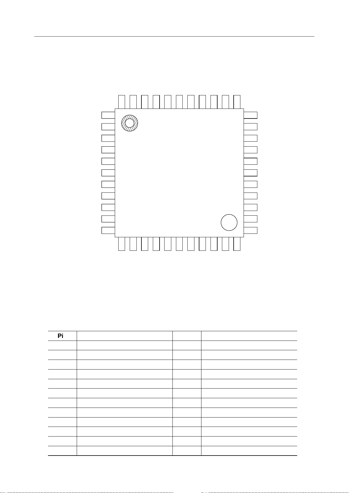
¡ Semiconductor MSC1951-01
(GND)
DD
SS
AD16
AD15
AD14
AD13
44
43
42
41
V
40
V
39
PNT
38
TAIL
37
SGP
36
SGO
35
SGN
34
NC
AD12
AD11
AD10
AD 9
AD 8
AD 7
AD 6
AD 5
AD 4
AD 3
10
11
1
2
3
4
5
6
7
8
9
22
21
20
19
18
17
16
15
14
13
12
AD 2
AD 1
(GND)
DD
V
A
POR
(GND)
DD
V
DATA
SCLK
SGA
SGB
NC
33
32
31
30
29
28
27
26
25
24
23
SGM
SGL
SGK
SGJ
SG I
SG H
SGG
SGF
SGE
SGD
SGC
Pin Function
1 No-connection pin
2 Digit output pin 12
~
~
13 Digit output pin 1
14 GND
15 TEST pin
16 POWER-ON-RESET pin
17 GND
18 Data input pin
19 Shift clock pin
20 Segment output pin A
21 Segment output pin B
NC : No-connection pin
44-Pin Plastic QFP
Pin Function
22 No-connection pin
23 Segment output pin C
~
36 Segment output pin P
37 TAIL output pin
38 POINT output pin
39 GND
40 Power supply (5V)
41 Digit output pin 16
~
44 Digit output pin 13
~
~
5/17
¡ Semiconductor MSC1951-01
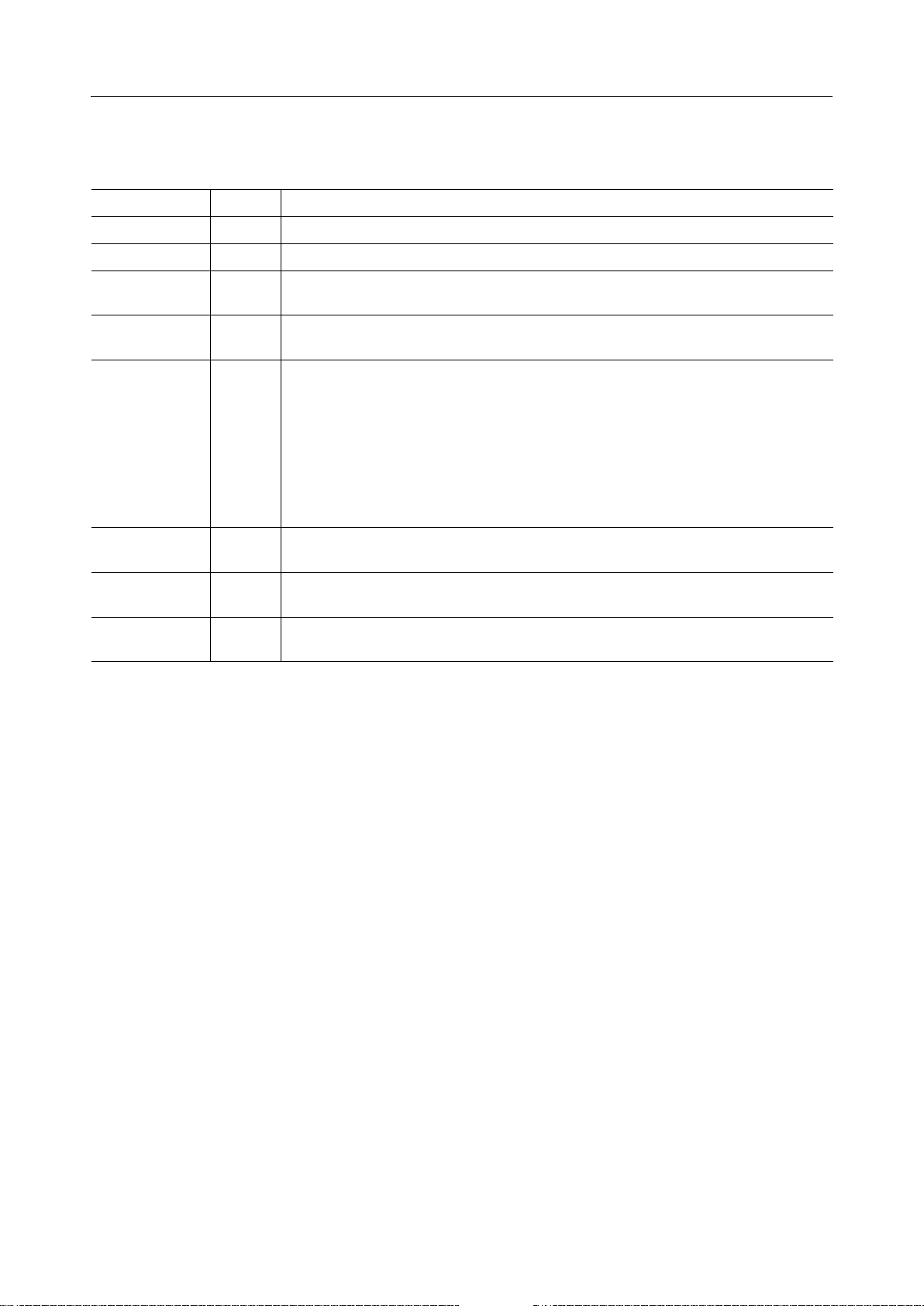
PIN DESCRIPTIONS
Symbol Type Description
V
SS
V
DD
DATA I
SCLK I
POR I
A I/O
AD16 to AD1 O
SGA to SGP
TAIL, PNT
—
—
Power supply pin
GND pin
Serial data Input of display data/control data
Input from MSB
Shift clock signal input of shift register
Shifts data at the falling edge of SCLK
Power-on-reset input. Input of "H" level into this pin with the power turned on
initializes this IC.
The internal state after the initialization is as follows:
1) AD1 to AD16, SGA to SGP, TAIL and PNT output are in the off state.
2) The duty cycle is set to "0".
3) The digit counter value is set to 16 digits.
4) The buffer pointer is set to AD1.
5) Pin "A" is in the output mode.
Usually used as an output mode, and outputs 1/5 of the internal oscillation
frequency. In the test mode, operates as an input pin.
Grid output pin
The output configuration is an emitter follower.
O
Segment output pin
The output configuration is an emitter follower.
6/17
 Loading...