E2C0024-27-Y4
¡ Semiconductor
This version: Nov. 1997
Previous version: Jul. 1996
MSC1230¡ Semiconductor
MSC1230
111-Bit 2/3-Duty Controller/Driver with Digital Dimming Function
GENERAL DESCRIPTION
The MSC1230 is a Bi-CMOS display driver with digital dimming function. It enables switching
between 1/3-duty vacuum fluorescent (VF) display tube and universal VF display tube by pin
control.
The MSC1230 consists of a 112-bit shift register, a 111-bit latch, a 10-bit digital dimming circuit,
37 segment drivers, and 3 grid drivers.
The MSC1230 provides an interface with a microcomputer only by three signal lines: CS,
DATA-IN, and CLOCK.
By using the chip select function, the DATA-IN and CLOCK signal lines can be shared
by other peripheral circuits.
FEATURES
• Power supply voltage :
• Operating temperature range : Ta=–40 °C to +85 °C
• 37-segment driver outputs : IOH=–6 mA at VOH = VDD –0.8 V
• 3-grid driver outputs : IOH=–30 mA at VOH = VDD –0.8 V
• Built-in digital dimming circuit (10-bit resolution)
• Switchable between 1/3-duty VF display tube and universal VF display tube*
When SEL pin is left open : Selects universal VF display tube (The grids GRID1, GRID2,
and GRID1+GRID2 are turned on repeatedly in this order)
When SEL pin is used at 0 V : Selects 1/3-duty VF display tube (The grids GRID1, GRID2,
and GRID3 are turned on repeatedly in this order)
• Built-in oscillation circuit (external R and C)
• Built-in Power-On-Reset circuit
• Package:
56-pin plastic QFP (QFP56-P-910-0.65-2K)(Product name: MSC1230GS-2K)
* A universal VF display tube is a display tube for which, like a gate array, the user can freely
design characters and patterns on the master layer (grid). (Pattern can be created without gaps
between grids.)
Since the outline dimensions of the display tube and the grid layout are predetermined,
desired patterns can be displayed in a short time.
The universal VF display tube is used for the display parts for audio equipment, household
appliances, and automobile equipment.
VDD=8 V to 18 V (built-in 5 V regulator for logic circuit)
1/13

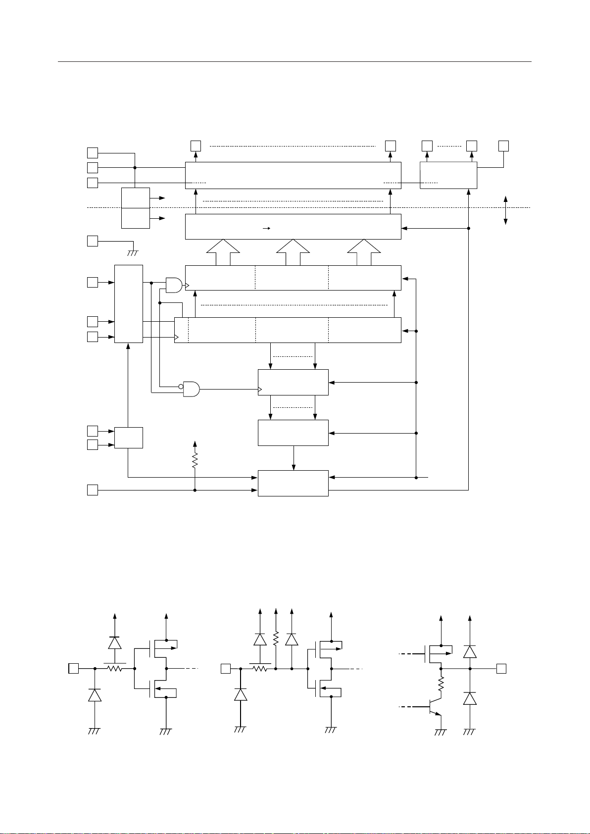
BLOCK DIAGRAM
MSC1230¡ Semiconductor
V
DD1
V
DD2
DGND
LGND
CS
DATA-IN
CLOCK
OSC0
OSC1
5V
REG.
POR
Control
Circuit
OSC
SEG37 SEG1 GRID3 GRID1
37-bit Segment Driver
5V
POR
37
75111 74 38 37 1
112 111 107106 97 96
5V
37bit data
111 37-Segment Control
3737
111-bit Latch
111-bit data
112-bit Shift Register
10-bit data
10-bit Latch
10-bit data
10-bit Digital
Diming
1
37
3-bit Grid Driver
1
V
3
DD
V
=8 - 18V
DD
VCC=5.0V
(Regurator)
SEL
112bits=0: Digital Dimming Mode
112bits=1: VF Data Input Mode
INPUT AND OUTPUT CONFIGURATION
l Schematic Diagram 1 of
Logic Portion Input Circuit
(5V Reg.)
GND
INPUT
V
DD
GND
l Schematic Diagram 2 of
Logic Portion Input Circuit
V
DD
COLn
GND
Timing
Generator
(5V Reg.)
GND
POR
l Schematic Diagram of
Driver Output Circuit
V
GND
DD
V
DD
OUTPUT
GND
2/13

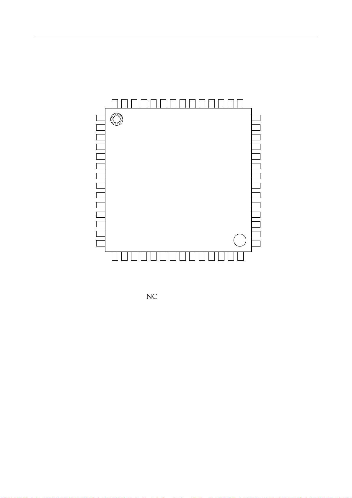
PIN CONFIGURATION (TOP VIEW)
MSC1230¡ Semiconductor
SEG19
SEG20
SEG21
SEG22
SEG23
SEG24
SEG25
SEG26
SEG27
SEG28
SEG29
10
11
SEG30 12
SEG31 13
SEG32 14
SEG17
SEG18
55
56
SEG15
SEG16
53
54
DD2
V
SEG14
51
52
NC
50
DGND
49
1
2
3
4
5
6
7
8
9
22
21
20
15
16
17
18
19
NC
48
23
DD1
V
47
24
SEG13
SEG1245
46
25
26
SEG1144
27
SEG1043
28
42
41
40
39
38
37
36
35
34
33
32
31
30
29
SEG9
SEG8
SEG7
SEG6
SEG5
SEG4
SEG3
SEG2
SEG1
NC
GRID1
GRID2
GRID3
V
DD3
SEG34
SEG33
NC
SEG36
SEG35
SEG37
LGND
NC: No connection
56-Pin Plastic QFP
NC
OSC1
OSC0
SEL
CS
CLOCK
DATA-IN
3/13

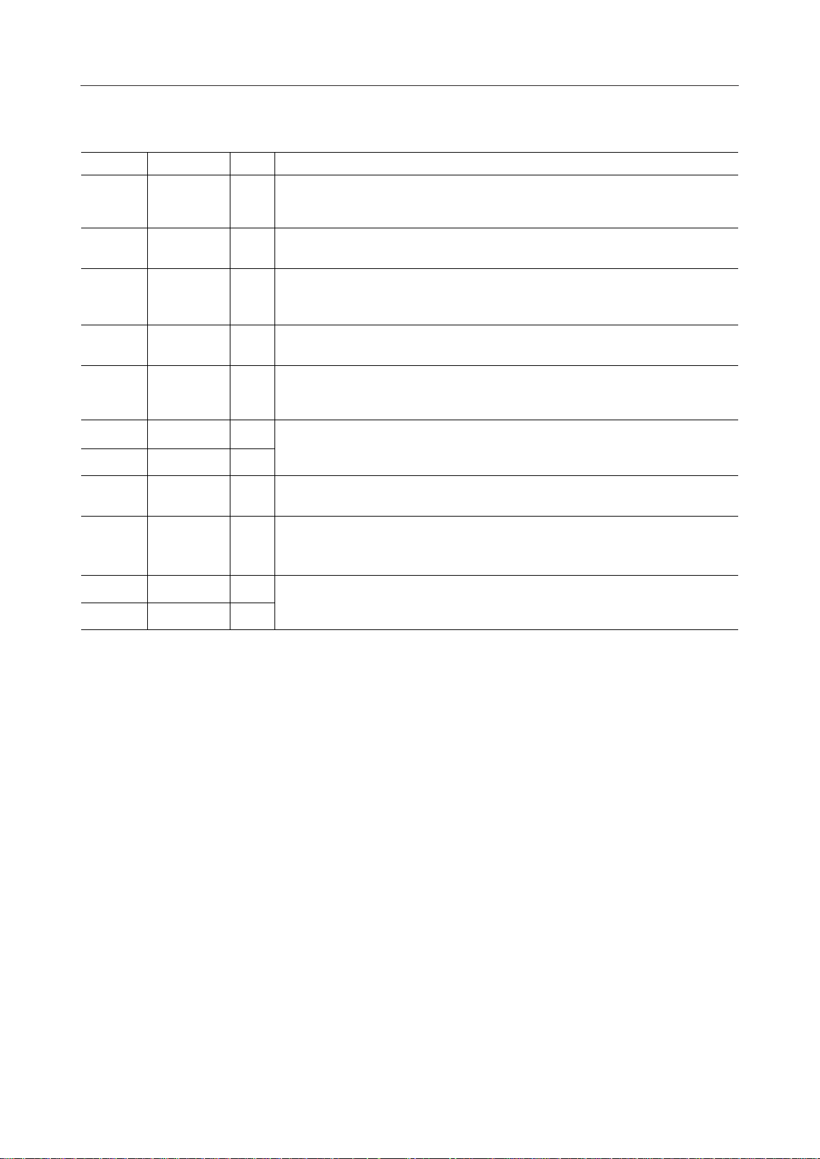
PIN DESCRIPTION
MSC1230¡ Semiconductor
Pin
34 to 46,
Symbol Type Decription
SEG1 to 37 O Output pins for segment signals for driving VF display tube.
52 to 56,
1 to 19
30 to 32
25
GRID1 to 3 O Output pins for grid signals for driving VF display tube.
SEL I When at a "L" level, this pin selects 1/3-duty VF display tube.
28
27
24
23
26
47
51
29
49 —
21 —
CLOCK
OSC0
OSC1
CS
V
DD1
V
DD2
V
DD3
DGND
LGND
The GRID3 output is not used when the universal VF display tube is used.
When at a "H" level (or when used in the open state), this pin selects universal
VF display tube.
IDATA-IN
Pin for series data input from microprocessor.
Data is input to the shift register on the rising edge of the CLOCK signal.
I
Serial clock input pin.
Data is input through the DATA-IN pin at the rising edge of the serial clock.
RC oscillator connecting pins.
I
Connect a resistor between the OSC1 and OSC0 pins and a capacitor between
O
the OSC0 pin and the ground.
I
Chip select input pin. Circuit operation is valid when this pin is at a "L" level.
Power supply pins. When using these pins, connect each of them to the power
—
supply.
Ground pins for driver and logic. These pins can be connected with each other
when they are used.
4/13
 Loading...