E2C0023-27-Y3
¡ Semiconductor MSC1218
¡ Semiconductor
This version: Nov. 1997
Previous version: Jul. 1996
MSC1218
63-Bit Triplex Controller/Driver with Digital Dimming Function
GENERAL DESCRIPTION
The MSC1218 is a Bi-CMOS driver for 1/3 duty vacuum fluorescent display tube.
It contains a 64-bit shift register, a 63-bit latch, a 10-bit digital dimming circuit, and three grids.
The MSC1218 has only three microcontroller interface signal lines: CS, D-IN, and CLOCK.
The chip select function enables the D-IN and CLOCK lines to be shared with other peripheral
circuits.
FEATURES
• Power supply Voltage : 8 to 18V (built-in 5V regulator for logic circuit)
• Operating temperature : -40 to +85°C
• 21-segment driver outputs : IOH=–6mA at VOH=VDD–0.8V
• 3-grid driver outputs : IOH=–16mA at VOH=VDD–0.8V
• Built-in digital dimming circuit : 10-bit resolution
• Built-in RC oscillation circuit : External R and C
• Built-in Power-On-Reset circuit
• Package:
32-pin plastic SSOP(SSOP32-P-430-1.00-K) (Product name: MSC1218GS-K)
1/12

¡ Semiconductor MSC1218
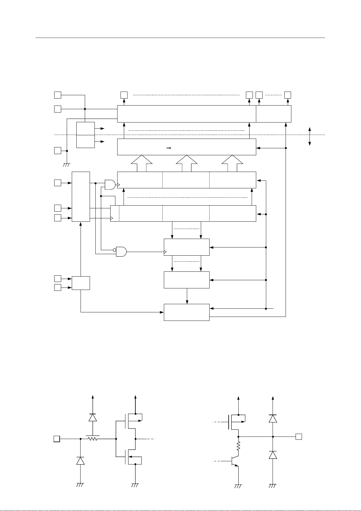
BLOCK DIAGRAM
SEG21 SEG1 GRID3 GRID1
V
DD1
V
DD2
5V
REG.
5V
21-bit Segment Driver 3-bit Grid Driver
21-bit data
V
DD
=8 - 18V
GND
CS
DATA-IN
CLOCK
OSC0
OSC1
POR
Control
Circuit
OSC
POR
21
64 63 59 58 49 48
63 21-Segment Control
2121
4363 42 22 21 1
63-bit Latch
63-bit data
64-bit Shift Register
10-bit data
10-bit Latch
10-bit data
10-bit Digital
Diming
Timing
Generator
1
VCC=5.0V
(Regurator)
21
1
POR
64 bits=0: Digital Dimming Mode
64 bits=1: VF Data Input Mode
INPUT AND OUTPUT CONFIGURATION
• Schematic Diagrams of Logic Portion Input
Circuit
INPUT
V
DD
GND
(5V Reg.)
GND
• Schematic Diagrams of Driver Output Circuit
V
GND
DD
V
GND
DD
OUTPUT
2/12

¡ Semiconductor MSC1218
PIN CONFIGURATION (TOP VIEW)
SEG 1
SEG 2
SEG 3
SEG 4
SEG 5
SEG 6
SEG 7
SEG 8
SEG 9
SEG10
SEG11
SEG12
SEG13
SEG14
SEG15
SEG16
SEG17
1
2
3
4
5
6
7
8
9
10
11
12
13
14
15
16
32
31
30
29
28
27
26
25
24
23
22
21
20
19
18
17
GRID1
GRID2
GRID3
V
DD2
OSC0
OSC1
GND
DATA-IN
CLOCK
CS
V
DD1
SEG21
SEG20
SEG19
SEG18
32-Pin Plastic SSOP
3/12

¡ Semiconductor MSC1218
PIN DESCRIPTIONS
Pin
32,
1 - 20
29 - 31
24
23
27
26
22
21
28
25 —
Symbol Type Decription
SEG1 - 21 O Output pins for segment signals for driving VF display tube (anode).
GRID1 - 3 O Output pins for grid signals for driving VF display tube (grid).
CLOCK
OSC0
OSC1
CS
V
DD1
V
DD2
GND
ID-IN
Serial data input pin (positive logic).
Shift clock input pin.
I
Serial data shifts at the rising edge of CLOCK.
RC oscillator connecting pins. Oscillation frequency is 3.2MHz.
I
Connect a resistor between the OSC1 and OSC0 pins and a capacitor between
O
the OSC0 pin and the ground.
Chip select input pin. Data transfer is inhibited when this pin is "H".
I
Power supply pins. When using these pins, connect each of them to the power
supply.
—
Ground pin.
4/12
 Loading...