


E2C0022-27-Y3
¡ Semiconductor
This version: Nov. 1997
Previous version: Jul. 1996
MSC1215-xx¡ Semiconductor
MSC1215-xx
¥¥
17
¥ 2 Duplex Driver with Dimming, Keyscan and A/D Converter Function
¥¥
GENERAL DESCRIPTION
The MSC1215-xx is a 1/2-duty vacuum fluorescent display tube driver implemented in BiCMOS technology. This LSI consists of a 37-bit shift register, 34 latches, an analog dimming
circuit, (a PWM conversion circuit), a 3¥4 keyscan circuit, a 6ch-6-bit A/D converter and 17
segment drivers, and 2-grid pre-drivers.
The MSC1215-xx has capabilities of displaying audio system frequencies and various informations on a VFD tube for the automobile application and also interfacing with keyboard inputs and
on an analog volume input.
For automobile audio systems, the front panel functions (such as a frequency display, keyboard
input and analog voltage input from a volume) can be accomplished by this IC.
The analog dimming/PWM conversion modes can be selected automatically for the brightness
control, so this IC is applicable to any type of automobile without any change of the specifications.
The interface with a MCU can be done only with 3 wires (CS, DATA I/O and CLOCK signals).
Also, DATA I/O and CLOCK signal lines can be shared with other peripherals because of chip
select function by CS signal.
FEATURES
• Power supply voltage : VDD=8 to 18 V
• Operating temperature range : Ta=–40 to +85°C)
• 17-segment driver outputs (IOH=–5mA at VOH=VDD–0.8 V)
• Built-in analog dimming circuit (6-bit resolution, user-programmable)
• Built-in PWM conversion circuit (Lamp PWM signal to vacuum fluorescent display PWM
signal)
• Built-in automatic-selection circuit for analog dimming/PWM conversion function
• Built-in 6ch 6-bit A/D converter
• Built-in 3 ¥ 4 Keyscan circuit
• Built-in oscillation circuit (external R and C, f
• Built-in Power-On-Reset circuit
• Package:
42-pin plastic DIP (DIP 42-P-600-2.54) (Product name: MSM1215-xxRS)
xx indicates the code number.
=3.3 MHz)
OSC
1/22

BLOCK DIAGRAM
MSC1215-xx¡ Semiconductor
SEG1 SEG17
V
DD
GND
PWMOUT
CS
DATA I/O
CLOCK
OSC0
OSC1
VK
VD
SW1
Regulator
Timing
OSC
+
-
D/A
P. O. R
5V
17 Segment
VF Tube Driver
34Æ17 Segment Control
bit 34-18
(Grid2)
L
D
34-bit Latch
bit34 bit1
34-bit Shift Register
R
Timing Generator
MUX Latch PWM
Select
Logarithm Counter
bit 17-1
(Grid1)
Grid
Pre-driver
3-bit
Latch
3-bit
S/R
Test
SW1 (VF Data)
SW2 (Keyscan)
SW3 (A/D)
Mode
Select
Test1-8
GRID1
GRID2
to PWM OUT
SW2
Read Enable
"H"at SW2 ON
Decoder
De-glitch PWM detector Look up table
SI
12-bit Presetable S/R
out
Set S S PE
444
4-bit
LLL
Latch
444
Timing
Generator
Row Col
321 3214
Detector
With 100kW pull-up resistor
6-bit dig. comp.
+
-
"H" at SW3 ON
Read Eable
Timing
Generator
PE
O
SW3
CH1
CH2
CH3
CH4
CH5
CH6
V
REF
Channel
Select
V
REF
6ch 6-bit
A/D
& Logic
36-bit
S/R
2/22
INPUT AND OUTPUT CONFIGURATION
GND
(5V Reg.)
V
DD
GND
DATAI/O
GND
(5V Reg.)
GND
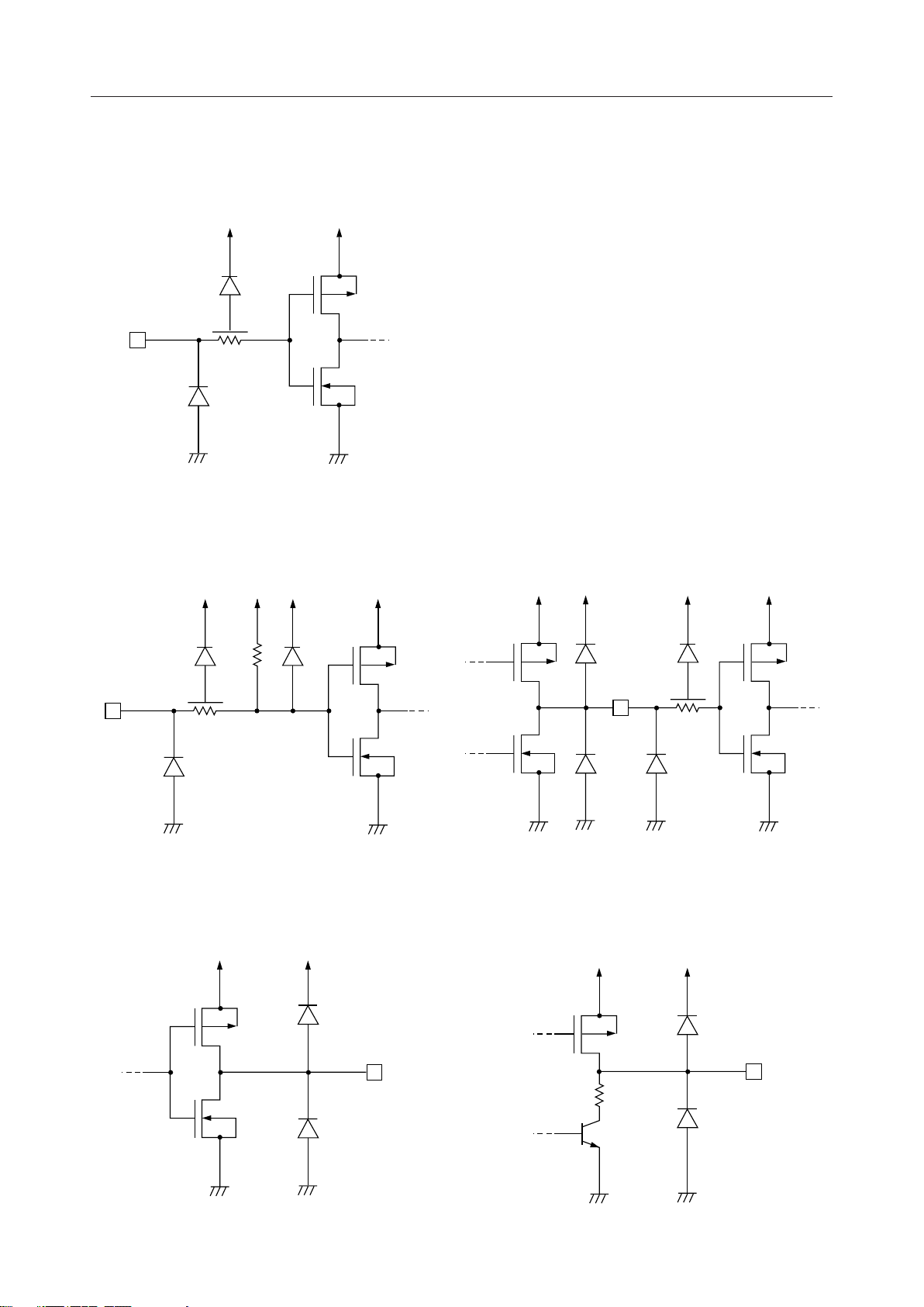
• Schematic Diagrams of Logic Portion Input Circuit 1
MSC1215-xx¡ Semiconductor
INPUT
V
DD
GND
(5V Reg.)
GND
• Schematic Diagrams of Logic Portion Input
Circuit 2
V
DD
(5V Reg.)
• Schematic Diagrams of Logic Portion Input/
Output Circuit
COLn
GND
GND
• Schematic Diagrams of Logic Portion Output
Circuit
(5V Reg.)
(5V Reg.)
OUTPUT
• Schematic Diagrams of Driver Output Circuit
V
DD
V
DD
OUTPUT
GND
GND
GND
GND
3/22

PIN CONFIGURATION (TOP VIEW)
MSC1215-xx¡ Semiconductor
COL4
GRID1
GRID2
SEG 1
SEG 2 5
SEG 3 6
SEG 4
SEG 5
SEG 9 9 CH334
SEG10 10
SEG11 11 CH132
SEG12
SEG13
SEG14 15 VK28
SEG15 16 DATA I/O
1 COL3
2 COL2
3
4
7
8
VDD12 GND31
13
14
42
41
40
39
38
37
33
27
COL1
VD
V
REF
CH6
CH536
CH435
CH2
OSC030
OSC129
SEG16 17 CS26
SEG17 18 CLOCK25
SEG 6 19 ROW 1
SEG 7 20 ROW 2
SEG 8
21 ROW 322
24
23
42-Pin Plastic DIP
4/22

ABSOLUTE MAXIMUM RATINGS
MSC1215-xx¡ Semiconductor
Parameter
Supply Voltage
Input Voltage (1)
Input Voltage (2)
Power Dissipation
Storage Temperature
Symbol Condition Rating Unit
T
V
V
V
DD
IN1
IN2
P
STG
All inputs except VK
D
—
VK
Ta=85°C
— –55 to +150
RECOMMENDED OPERATING CONDITION
Parameter
Supply Voltage
Operating Temperature
High Level Input Voltage (1)
High Level Input Voltage (2)
Low Level Input Voltage
Clock Frequency
OSC Frequency
Frame Frequency 200f
Symbol Typ. Unit
V
DD
T
OP
V
IH1
V
IH2
V
IL
f
c
f
osc
FR
Condition
—
—
All inputs except VK
VK
All inputs
—
R=4.7 kW, C=10 pF
–0.3 to +20 V
–0.3 to +6
–0.3 to +V
400
DD
V
V
mW
°C
Min.
8
–40
3.8
3.8
0
—
—
—
—
—
—
—
—
3.33
Max.
18
85
5.5
V
DD
0.8
250
—
V
°C
V
V
V
kHz
MHz
——Hz—
5/22

ELECTRICAL CHARACTERISTICS
DC Characteristics
Parameter
"H" Input Voltage
"L" Input Voltage
"H" Input Current (1)
"H" Input Current (2)
"L" Input Current (1)
"L" Input Current (2)
"H" Output Voltage (1)
"H" Output Voltage (2) V
Symbol Min. Unit
V
IH
V
IL
I
IH1
I
IH2
I
IL1
I
IL2
V
OH1
OH2
Condition
All inputs except VD
All inputs except VD
All inputs except COL1-4
=4.4 V
V
IN
COL1-4, V
=3.8 V
IN
All inputs except COL1-4
VIN=0 V
COL1-4, VIN=0 V
SEG, GRID
=–5 mA, VDD=9.5 V
I
OH1
DATA I/O, V
I
OH2
=9.5 V
DD
=–200 mA
Output open
MSC1215-xx¡ Semiconductor
(Ta=–40 to +85°C, V
Max.
3.8 V
—
–5
–70
–5
–160
V
-0.8
DD
4
4.5
=8 to 18V)
DD
—
0.8
5
–5
5
–10
—
—
—
V
mA
mA
mA
mA
V
V
V
"L" Output Voltage (1)
"L" Output Voltage (2)
Current Consumption
V
OL1
V
OL2
DD
SEG,GRID, V
I
OL1
I
OL1
I
OL1
DATA I/O, ROW1-3
=9.5 V, I
V
DD
=3.3 MHz, no loadI
f
osc
DD
=500 mA
=200 mA
=2 mA
=200 mA
OL2
=9.5 V
—
—
—
—
—
2
1
0.3
0.8
20
V
V
V
V
mA
6/22

Switching Characteristics
Parameter
Oscillation Frequency f
Clock Frequency
Clock Pulse Width
Data Set-up Time
Data Hold Time
CS Pulse Width
CS Off Time
CS Pulse Width t
CS Off Time
CS Set-up Time
CS-clock Time
CS Hold Time
Clock-CS Time
DATA Output Delay
CLCOK-DATA Out Time
Symbol Min. Unit
osc
f
t
cw
t
DS
t
DH
t
CSW
t
CSL
RCSW
t
RCSL
t
CSS
t
CSH
t
PD
MSC1215-xx¡ Semiconductor
(Ta=–40 to +85°C, V
Condition
— MHz4.52
c
—
—
—
—
Except reset mode
Except reset mode
—
1.3
1
200
8
32
Reset mode 4
Reset mode
—
—
—
4
2
2
—
=8 to 18 V)
DD
Max.
250
—
—
—
—
—
—
— ms
—
—
1
kHz
ms
ms
ns
ms
ms
ms
ms
ms
ms
SEG & GRID Outputs Delay
t
ODS
CL=100 pF
Time from CS
Slew Rate (All Drivers)
t
R
=100 pF
C
L
t=20% to 80% or
80% to 20% of V
Power on Timing —
t
PCS
DD
—
—
300
—
8
5
ms
ms
ms
7/22
 Loading...