E2C0020-29-53
¡ Semiconductor MSC1209
¡ Semiconductor
This version: May 1999
Previous version: Nov. 1997
MSC1209
42-Bit Vacuum Fluorescent Display Tube Driver with Digital Dimming Function
GENERAL DESCRIPTION
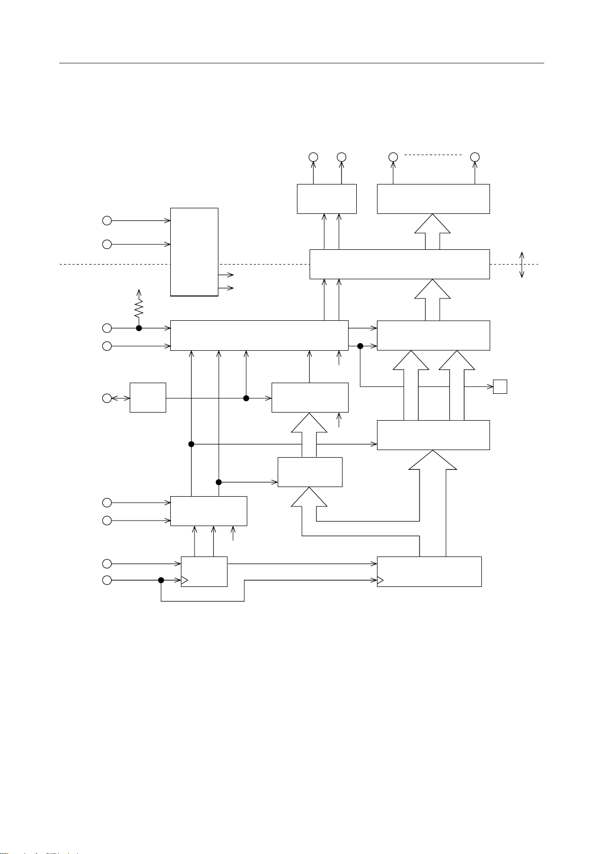
The MSC1209 is a Bi-CMOS display driver for a 1/2-duty vacuum fluorescent display tube. The
MSC1209 consists of an 84-bit shift register, an 84-bit latch circuit, a 10-bit digital dimming circuit,
42-bit segment drivers, a 2-bit grid circuit, and a cascade control circuit.
The MSC1209 is interfaced with a microcontroller by using three signal lines of LOAD, CLOCK,
and DATA. The cascaded MSC1209 ICs can share LOAD, CLOCK, and DATA.
FEATURES
• Power supply voltage: 8V to 18V (Built-in 5V regulator for logic)
• Operating temperature range: –40 to +105°C
• Driving 42 segments directly: VOH=VDD–0.5V at IOH=–3.0mA (VDD=15.0V)
• Built-in digital dimming circuit
10-bit resolution
Programmable in the duty range of 0/2048 (0%) to 1016.5/2048 (49.6%)
• 3 interfaces with microcontroller: LOAD, CLOCK, DATA
• Cascade connection available
(The cascaded MSC1209 ICs can share LOAD, CLOCK, and DATA.)
• Built-in oscillation circuit with an external capacitor (a single pin is used)
• Built-in power-on reset circuit
• Package:
56-pin plastic QFP (QFP56-P-910-0.65-2K) (Product name: MSC1209GS-2K)
1/15

¡ Semiconductor MSC1209
BLOCK DIAGRAM
SEG42SEG1GRID2GRID1
V
DD
V
BLANK
MODEA
OSC
MODEB
LOAD
SS
5V
OSC
Voltage
Regulator
LOAD
Timing Control
5V
POR
Timing Generator
Digital Dimming
L
2-bit
Grid Driver
10-bit
10-bit Latch
42-bit Segment Driver
Level Shifter
POR
POR
L
10-bits (Q1 to Q10)
Multiplexer
84-bit Latch
84 bits
VDD=8 to 18V
=5.0V
V
CC
(Regulator)
SEL
DATA
CLOCK
D
2-bit S/R
POR
D
Q1-Q84
84-bit Shift Register
2/15

¡ Semiconductor MSC1209
INPUT AND OUTPUT CONFIGURATION
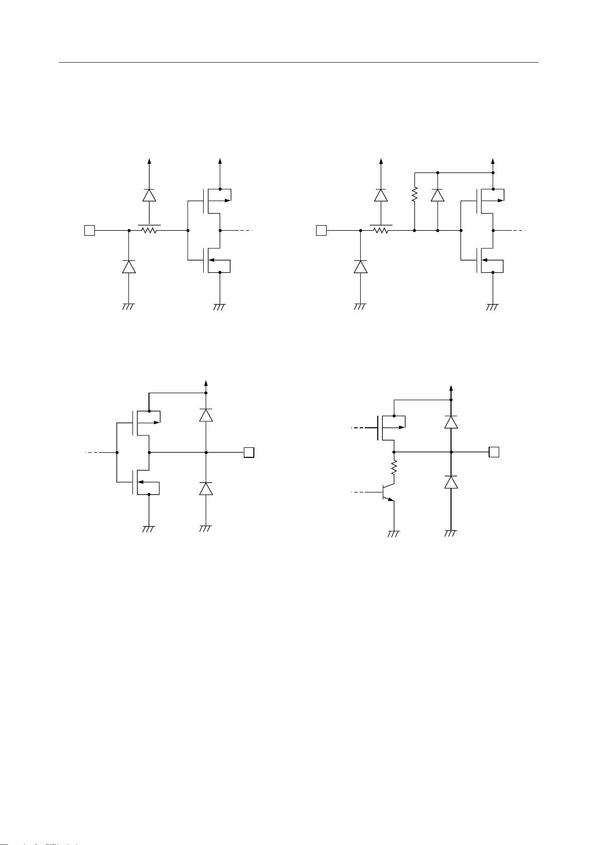
• Schematic Diagram of Logic Portion Input
Circuit 1
INPUT
V
DD
V
SS
(5V Reg.)
V
SS
• Schematic Diagram of Logic Portion Output
Circuit
(5V Reg.)
• Schematic Diagram of Logic Portion Input
Circuit 2
SEL
V
DD
V
SS
(5V Reg.)
V
SS
• Schematic Diagram of Driver Output Circuit
V
DD
V
SS
OUTPUT
OUTPUT
V
SS
V
SS
V
SS
3/15

¡ Semiconductor MSC1209
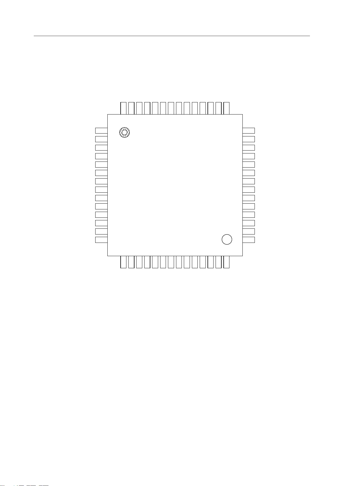
PIN CONFIGURATION (TOP VIEW)
SEG 4
SEG 5
SEG 6
SEG 7
SEG 8
SEG 9
SEG10
SEG11
SEG12
SEG13
SEG14
SEG15
SEG16
SEG17
10
11
12
13
14
SEG 1
SEG 2
SEG 3
56555453525150494847464544
1
2
3
4
5
6
7
8
9
15
SEL
MODEB
NC
DATA
CLOCK
LOAD
21222324252627
VSSMODEA
OSC
BLANK
GRID2
43
28
42
41
40
39
38
37
36
35
34
33
32
31
30
29
GRID1
V
DD
SEG42
SEG41
SEG40
SEG39
SEG38
SEG37
SEG36
SEG35
SEG34
SEG33
SEG32
SEG31
NC
SEG1816SEG1917SEG2018SEG2119SEG2220SEG23
NC: No connection
56-Pin Plastic QFP
SEG24
SEG25
SEG26
SEG27
SEG28
SEG29
SEG30
4/15

¡ Semiconductor MSC1209
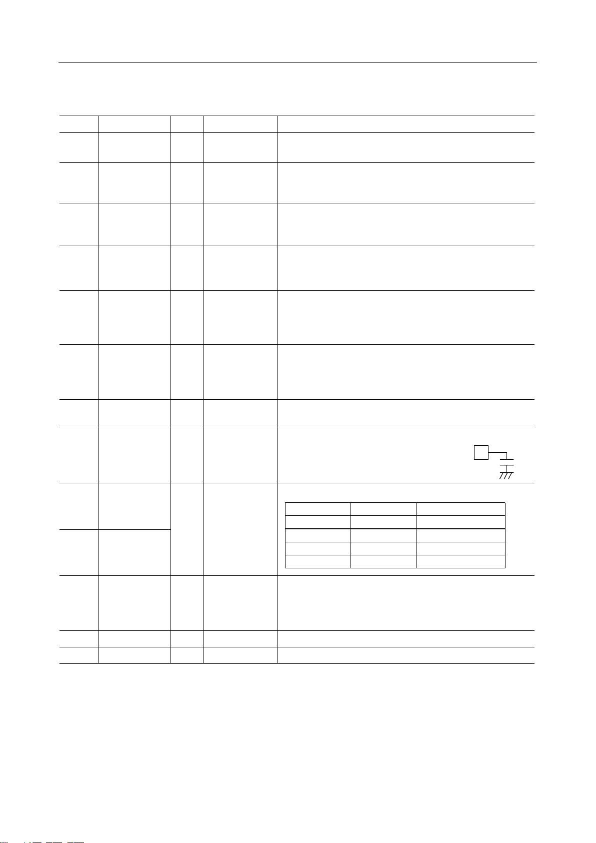
PIN DESCRIPTION
Pin Symbol
48 DATA
50
51 LOAD
1 to 20,
22 to 40,
54 to 56
42 GRID1
43 GRID2
44 BLANK
45 OSC
46 MODEA
52 MODEB
CLOCK
SEG1 to SEG42
Type
I
I
I
O
O
O
I
I/O
I
Connected to
Microcontroller
Microcontroller
Microcontroller
Anode electrode
of VFD tube
Grid electrode
of VFD tube
Grid electrode
of VFD tube
—
—
—
Description
Serial data input. (Positive logic)
Receives display data and dimming data.
Shift clock input.
Serial data is shifted on the rising edge of this shift clock
pulse.
Load pulse input.
The load signal is input when the transfer of serial data is
completed.
Segment driver output.
Grid driver output. When this pin is set to "L", the display
goes on. Connect an external PNP transistor to this pin.
The segment data of the first bit (S1) to the 42nd bit (S42) is
valid in the 84-bit segment data.
Grid driver output. When this pin is set to "L", the display
goes on. Connect an external PNP transistor to this pin.
The segment data of the 43rd bit (S43) to the 84th bit (S84)
is valid in the 84-bit segment data.
Input with pull-up resistor for display blank. When this pin is
set to "L", the display goes off. (SEGn="L")
Input and output for oscillation. Connect an external
capacitor of 68pF.
The typical value of oscillating frequency
is 512kHz.
These pins specify the operating mode.
MODEA MODEB
0 0 Master Operation
10
01
1 1 Slave Operation
Operating Mode
Test Mode
Slave Operation
45
68pF
53 SEL
41 V
47 V
DD
SS
O
—
—
MODEA pin
at slave side
Power source
Power source
SEL pin of the master IC outputs switching signals for the
segment data that corresponds to the grid signals. The SEL
pin of the master IC is connected to the MODEA pin of the
slave IC.
Power supply pin (8V to 18V).
GND pin. (Ground)
5/15
 Loading...