E2C0017-27-Y2
¡ Semiconductor MSC1201-xx
¡ Semiconductor
This version: Nov. 1997
Previous version: Jul. 1996
MSC1201-xx
60-Bit VFD Tube Driver with Digital Dimming and PWM Conversion Function
GENERAL DESCRIPTION
The MSC1201-xx is a 1/2 duty vacuum fluorescent display tube driver implemented in Bi-CMOS
technology. This LSI consists of 64-bit shift registers, 64 latches, PWM conversion circuit, a digital
dimming circuit, 30-segment driver and 2-grid driver. As the MSC1201-xx has both a digital
dimming circuit and a PWM conversion circuit which converts PWM signal for lamp dimming
control to PWM signal for VFD tube dimming control, the dimming control can be realized
without any external circuit.
The interface with a MCU can be done only with 3 wires (CS, DATA and CLOCK signals). Also,
DATA and CLOCK signal lines can be shared with other peripherals because of chip select
function by CS signal.
For the general purpose code, the code number is -01. (Product name: MSC1201-01GS-2K)
For a custom code, the code number will be ordered at any time.
FEATURES
• Single supply voltage : VDD = 8 V to 18 V (built-in 5 V logic regurator)
• Operating temperature range : Ta = –40°C to +85°C
• 30-segment driver outputs (IOH = –6 mA at VOH = V
• 2-grid pre-driver outputs (IOH = –30 mA at VOH = V
• Built-in digital dimming circuit (11-bit resolution)
• Built-in oscillation circuit (external R and C, f
• Built-in Power-On-Reset circuit.
• Lamp PWM signal Æ Buil-in PWM conversion circuit for vacuum fluorescent display tube.
• Built-in RC Oscillation (external R and C)
• Correspondence between shift register and output segment is settable optionally using built
in mask programmable 30 ¥ 30 PLA.
• Package :
44-pin plastic QFP (QFP44–P–910-0.80–2K)(Product name: MSC1201-xxGS-2K)
= 2.0 MHz)
OSC
xx indicates the code number
DD
DD
– 0.8 V)
– 0.8 V)
1/20

¡ Semiconductor MSC1201-xx
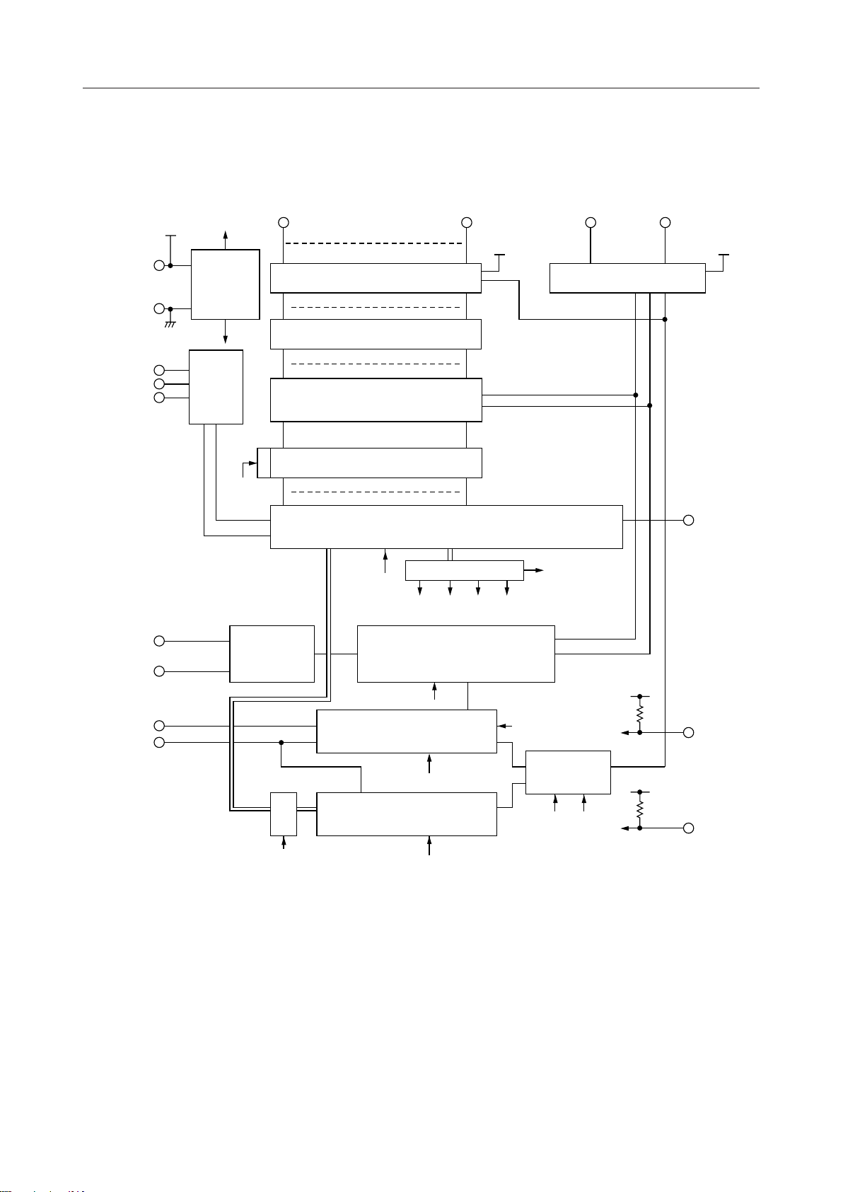
BLOCK DIAGRAM
V
DD
GND
CS
DATA
CLOCK
5 V
5 V Reg
&
POR Circuit
POR
Control
Circuit
S1
SEG1
D
CK
30-Segment Driver
30 ¥ 30 PLA Matrix
Multiplexer
Latch
64-Bit Shift Register
D48-59
R
POR
SEG30 GRID1 GRID2
2-Grid Driver
M3 M2 M1 M0
Mode Selector
S1 S2 S3 S4
Test Mode
DATA OUT
OSC0
OSC1
PWMIN
VK
RC
OSC
S2
Timing Generator
R
POR
PWM Conversion Circuit
R
POR
Digital Dimming Circuit
R
POR
S2
Selector
S3 S4
INH
TEST1
2/20

¡ Semiconductor MSC1201-xx
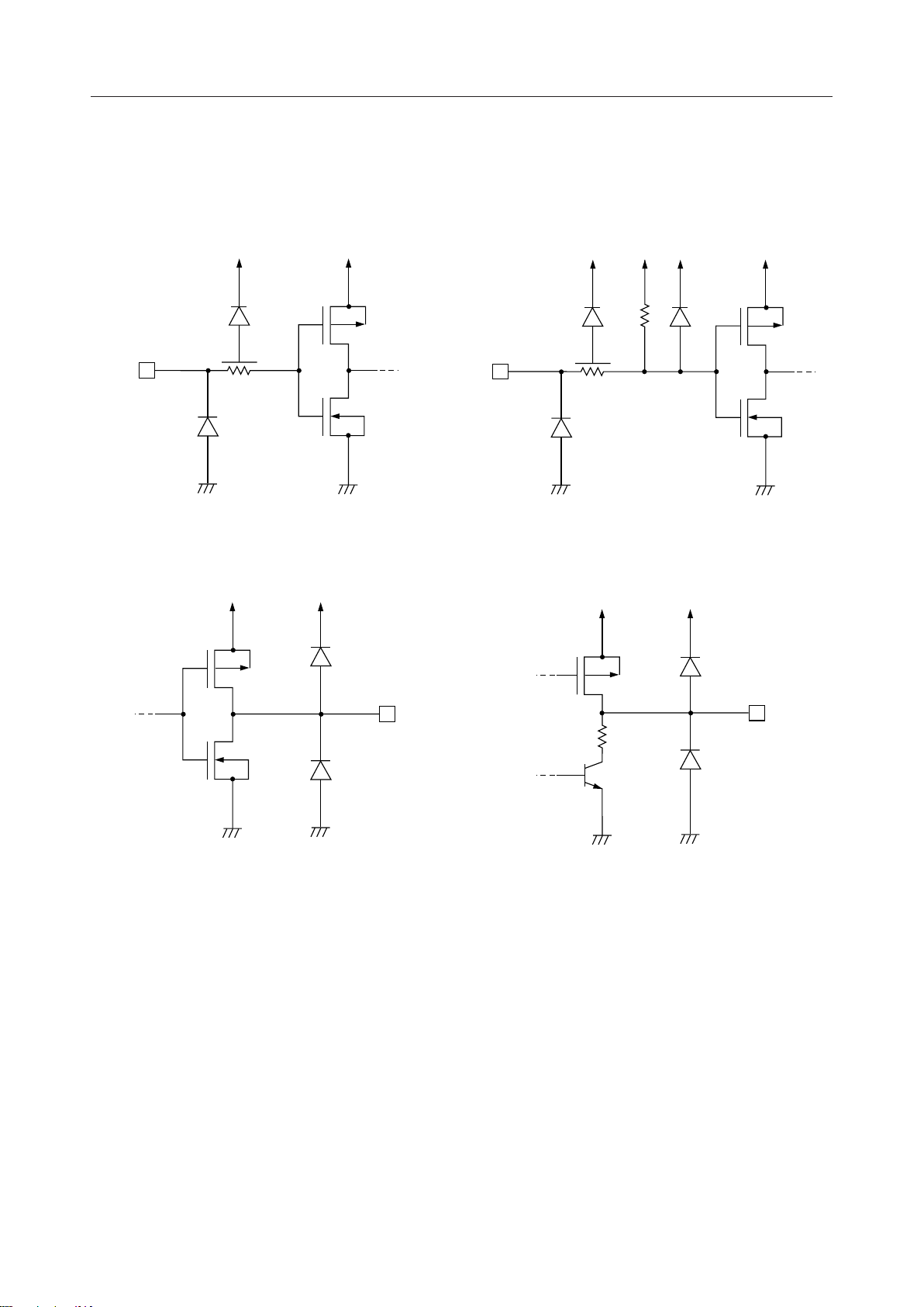
INPUT AND OUTPUT CONFIGURATION
• Schematic Diagrams of Logic Portion Input
Circuit 1
INPUT
V
DD
GND
(5V Reg.)
GND
• Schematic Diagrams of Logic Portion Output
Circuit
(5V Reg.)
(5V Reg.)
• Schematic Diagrams of Logic Portion Input
Circuit 1
TEST1
INH
V
DD
GND
(5V Reg.)
GND
• Schematic Diagrams of Driver Output Circuit
V
DD
V
DD
GND
GND
OUTPUT
GND
OUTPUT
GND
3/20

¡ Semiconductor MSC1201-xx
PIN CONFIGURATION (TOP VIEW)
SEG11
SEG12
SEG13
SEG14
SEG15
SEG16
SEG17
SEG18
SEG19
SEG20
SEG21
34
35
36
37
38
39
40
41
42
43
44
SEG10
SEG22
SEG23
1
2
33
32
SEG9
SEG24
SEG25
SEG26
SEG27
SEG28
SEG29
SEG30
GRID1
GRID2
10
11
3
4
5
6
7
8
9
21
20
19
18
17
16
15
14
13
12
V
DD
VK
OSC0
TEST1
OSC1
44-Pin Plastic Package
GND
CS
DATA
CLOCK
INH
31
30
29
28
27
26
25
24
23
22
PWM IN
SEG8
SEG7
SEG6
SEG5
SEG4
SEG3
SEG2
SEG1
DATAOUT
4/20

¡ Semiconductor MSC1201-xx
PIN DESCRIPTIONS
Pin Symbol
1-9
24-44
10, 11
16
15
18
20
19
23
22
14
SEG1-30
OSC0
OSC1
CS
DATA
CLOCK
DATA
OUT
PWMIN
VK
I/O
Segment output pin for VFD
O
OGRID1, 2 Grid 1 and Grid 2 output pins for VFD
I
RC oscillation pins. Connect a resistor between OSC1 and OSC0 pin and a capacitor
between OSC0 and GND pin.
O
Chip select input. Only when the high level is input to this pin, interfacing with a MCU
I
is available through "CLOCK" and "DATA" pins.
Therefore, 2-signal lines of "CLOCK" and "DATA" can be shared with other peripherals.
Input which receives display data and digital dimming data from a MCU. Data is
I
shifted in at the rising edge of the shift clock.
Serial clock input. Data that is input through "DATA" pin is input and output by
I
synchronization with the rising edge of the serial clock.
O
Serial data output. Data is shifted out at the rising edge of the serial clock with the
delay of 64-bit time. This pin is used for cascading this LSI with other drivers such
as a LED driver.
PWM signal input.
I
I
Dimming select input. When the high level is input, daylight-mode output duty cycle
is about 100% for each grid time for PWM conversion and digital dimming mode.
When the low level is input, the dark-mode output duty cycle is determined by the
duty cycle of the PWM signal input to PWM IN and the digital dimming output duty
cycle is determined by digital dimming data.
Description
21
13
12
17
INH
TEST1
V
DD
GND
I
Blank Display input with a built-in pull-up resistor. When set to "L", all the drivers
output "L". When display duly is not controlled by this signal, leave this pin open.
I
Test signal input pin. As this pin is used for shipping test of the LSI, leave open in the
normal operation mode.
—
Power Supply
— Ground
5/20

¡ Semiconductor MSC1201-xx
ABSOLUTE MAXIMUM RATINGS
Parameter Symbol Condition Rating Unit
Supply Voltage V
Power Dissipation P
DD
IN
STG
D
—
All inputsInput Voltage V
—Storage Temperature Range T
Ta = 85°C
RECOMMENDED OPERATING CONDITIONS
Parameter Symbol Condition Max. Unit
Supply Voltage V
High Level Input Voltage (1) V
High Level Input Voltage (2) V
High Level Input Voltage (3) V
Low Level Input Voltage (1) V
Low Level Input Voltage (2) V
Clock Frequency f
DD
IH1
IH2
IH3
IL1
IL2
C
OSC
FR
op
All inputs except OSC0, VK
All inputs except OSC0
R = 4.7kW, C=22pFOSC Frequency f
f
OSC
—
VK
OSC0
OSC0
—
= 2 MHzFrame Frequency F
—Operating Temperature Range T
–0.3 to +20 V
–0.3 to +6 V
–65 to +150 °C
0.4 W
Min.
8
3.8
Typ.
—
18 V
5.5 V—
V
DD
5.5 V—4.5
0.8 V—0
0.5 V—0
250 kHz——
— MHz2—
—Hz224—
85 ˚C—–40
V—3.8
6/20
 Loading...