FEDL1200V-03
FEDL1200V-03
¡ Semiconductor MSC1200-01/1200V-01
¡ Semiconductor
This version: Sep. 2000
Previous version: Nov. 1997
MSC1200-01/1200V-01
30-Bit Duplex Controller/Driver with Digital/Analog Dimming and Keyscan Functions
GENERAL DESCRIPTION
The MSC1200-01/1200V-01 is a Bi-CMOS display driver for 1/2-duty vacuum fluorescent
display tube. This device consists of a 64-bit shift register, latches, an analog dimming circuit,
a digital dimming circuit, a keyscan circuit, and drivers.
The interface with a microcomputer can be done only with four signal lines (CS, DATA I/O,
CLOCK, and INT). Also, the DATA I/O and CLOCK signal lines can be shared with other
peripherals by using the chip select function.
FEATURES
• Power supply voltage : 8V to 18V (built-in 5V regulator for logic)
• Operating temperature range : –40°C to +85°C
• 30-segment driver outputs (IOH = –6mA at VOH = V
• Built-in analog dimming circuit (PWM: 12.5% Max at 6-bit resolution)
• Built-in digital dimming circuit (11-bit resolution)
• Built-in 5 x 6 keyscan circuit
• Built-in RC oscillation circuit (external R and C)
• Built-in power-on-reset circuit.
• The product name differs depending on the bonding option pin selected:
PWM OUT/BLANK IN : MSC1200-01
DATA OUT : MSC1200V-01
• Package :
56-pin plastic QFP (QFP56–P–910-0.65–2K) (Product name: MSC1200-01GS-2K/MSC1200V-01GS-2K)
DD
– 0.8V)
1/26

FEDL1200V-03
¡ Semiconductor MSC1200-01/1200V-01
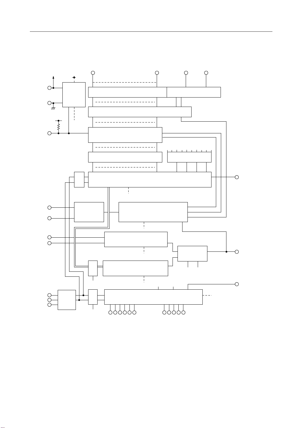
BLOCK DIAGRAM
V
DD
GND
TEST1
OSC0
OSC1
V
PARK
V
DIM
5V
5V
Regulator
&POR
POR
S1, S6, S7, S8
SEG1
R/C
OSC
D
CK
SEG30 GRID1 GRID2
30 Segment Drivers Grid Driver
PLA (32 ¥ 32 Matrix)
Multiplexer
Bit Latch Mode Selector
64-Bit Shift Register
M3 M2 M1 M0
R
Timing Generator
R
Analog Dimming
R
Selector
Digital Dimming
R
S2, S7, S3, S8
SAS9S8S7S6S5S4S3S2S1
DATA OUT
(Optional)
PWM OUT/
BLANK IN
(Optional)
CS
DATAI/O
CLOCK
Control
Circuit
S5, S6, S9
SAS9S4
5 ¥ 6 Keyscan Circuit
10325410324
ROWCOLUMN
INT
R
2/26

FEDL1200V-03
¡ Semiconductor MSC1200-01/1200V-01
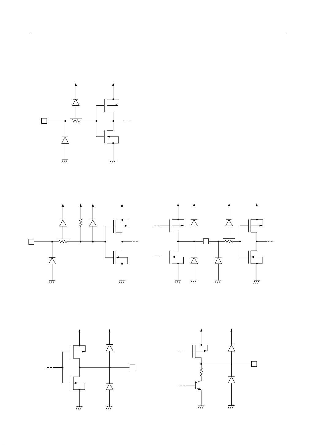
INPUT AND OUTPUT CONFIGURATION
• Schematic Diagrams of Logic Portion Input Circuit
INPUT
V
DD
GND
(5V Reg.)
GND
• Schematic Diagrams of Logic Portion Input
Circuit 2
TEST1
COLn
V
DD
(5V Reg.)
• Schematic Diagrams of Logic Portion Input/
Output Circuit
(5V Reg.)
DATAI/O
V
DD
(5V Reg.)
GND
GND
• Schematic Diagrams of Logic Portion Output
Circuit
(5V Reg.)
GND
(5V Reg.)
OUTPUT
GND
GND
GND
GND
GND
• Schematic Diagrams of Driver Output Circuit
V
GND
DD
V
GND
DD
OUTPUT
3/26

FEDL1200V-03
¡ Semiconductor MSC1200-01/1200V-01
PIN CONFIGURATION (TOP VIEW)
GRID2
GRID1
SEG30
SEG29
SEG28
SEG27
SEG26
GND
SEG25
SEG24
SEG23
SEG22
SEG21
SEG20
56
55
54
53
52
51
50
49
48
47
46
45
44
43
V
DD
V
PARK
V
DIM
CS
CLOCK
DATA I/O
INT
TEST1
*1
COLUMN0
COLUMN1
COLUMN2
COLUMN3
COLUMN4
1
2
3
4
5
6
7
8
9
10
11
12
13
14
42
41
40
39
38
37
36
35
34
33
32
31
30
29
SEG19
SEG18
SEG17
SEG16
SEG15
SEG14
SEG13
SEG12
SEG11
SEG10
SEG9
SEG8
SEG7
SEG6
15
16
17
18
19
20
21
22
23
24
25
ROW0
COLUMN5
ROW1
ROW2
ROW3
ROW4
GND
OSC0
OSC1
SEG1
SEG2
56-Pin Plastic QFP
*1 Bonding option pin (DATA OUT or PWM OUT/BLANK IN)
26
SEG3
27
SEG4
28
SEG5
4/26

FEDL1200V-03
¡ Semiconductor MSC1200-01/1200V-01
PIN DESCRIPTIONS
Pin Symbol Description
1V
DD
Type
—
Power Supply
Day/night switching pin. When the high level is input, the IC enters the night
mode and the value determined by the analog or digital dimming circuit is
2V
PARK
I
used as the output duty. When the low level is input, the IC enters the day
mode and the output duty is about 100%.
Analog voltage input for determining the analog dimming value.
When the analog dimming circuit is used, the output duty is determined by
3V
DIM
I
the analog voltage to be input to this pin.
When only the digital dimming circuit is used, pull down this pin to GND.
Chip select input. Only when the high level is input to this pin, interfacing
with a microcomputer is available through "CLOCK" and "DATA I/O" pins.
4CS
I
Therefore, 2 signal lines of "CLOCK" and "DATA I/O" can be shared with other
peripherals.
Serial clock input. Data is input-output through "DATA I/O" pin at the rising
5
CLOCK
6 DATA I/O
I
edge of the serial clock.
Serial data input-output. This pin enters output mode only when the keyscan
I/O
mode is selected. It enters input mode when other mode is selected.
Interrupt signal output to microcomputer. When any key is pressed or
7 INT
released, key scanning is started. After the completion of the one cycle, this
O
pin goes to the high level and keeps the high level until keyscan stop mode is
selected.
Test signal input. As this pin has a built-in pull-up resistor, it must be left
open or pulled up in the normal operation mode. When the low level is input
8 TEST1
I
to this pin, SEG1-30 go to the high level, and GRID1 and GRID2 go to the
low level. (All segments go on.)
Serial data output. Selecting this pin specifies the MSC1200V-01. The data
9
DATA OUT
(Option)
from DATA I/O is shifted out on the rising edge of the shift clock with a delay
O
of 64 bits in the shift register. This pin can be used for connecting the IC with
a LED driver in series.
When the V
pin is at the high level, the pulse with the duty ratio determin-
PARK
ed by the analog or digital dimming circuit is output through this pin. When
PWM OUT/
9
BLANK IN
(Option)
this pin is at the low level, the pulse with the duty ratio determined by external
circuit is input to this pin. This pin has an internal active pull-up resistor,
I/O
which becomes active only when the V
V
pin is at the low level, this pin receives blanking signal from external
PARK
pin is at the low level. When the
PARK
circuits, so that output duty cycle can be controlled. Selecting this pin specifies the MSC1200-01.
5/26

FEDL1200V-03
¡ Semiconductor MSC1200-01/1200V-01
Pin Symbol Description
10-15
16-20
21, 49 GND Ground
22, 23
24-48,
50-54
55, 56 GRID1,2
COLUMN
0-5
ROW0-4
OSC0
OSC1
SEG1-30
Type
Return inputs from key matrix switch. A pull-up resistor is internally
connected to each of these pins so that they are at the high level except when
I
the low level is input by depression of a key. These pins are "L" active.
Key switch scanning outputs. Normally the low level is output through these
pins. When any key is depressed or released, keyscanning is started and is
continued until keyscan stop mode is selected. When the keyscan stop mode
O
is selected and then keyscanning is stopped, all outputs of ROW0-4 go back
to the low level.
—
Connecting pins for RC oscillation circuit. Connect a resistor between OSC1
I/O
and OSC0, and a capacitor between OSC0 and ground.
Segment signal output. Signals for driving VF display tube are output
O
through these pins.
Grid signal output. Signals for driving VF display tube are output through
these pins. Signals inverted with respect to grid signals are output.
O
Normally, these pins are connected to the external grid driver (PNP transistor
etc.) inputs.
6/26

FEDL1200V-03
¡ Semiconductor MSC1200-01/1200V-01
ABSOLUTE MAXIMUM RATINGS
Parameter Symbol Condition Rating Unit
Supply Voltage V
Input Voltage (1) V
Input Voltage (2) V
Power Dissipation P
DD
IN1
IN2
STG
—
All inputs except V
V
PARK
PARK
—Storage Temperature T
D
Ta = 85°C
–0.3 to +20 V
–0.3 to +6 V
–0.3 to VDD +0.3 V
–65 to +150 °C
400 mW
RECOMMENDED OPERATING CONDITIONS
Parameter Symbol Condition Max. Unit
Supply Voltage V
High Level Input Voltage (2) V
High Level Input Voltage (3) V
Low Level Input Voltage (1) V
Low Level Input Voltage (2) V
Clock Frequency f
DD
IH1
IH2
IH3
IL1
IL2
C
OSC
FR
op
—
All inputs except V
V
PARK
OSC0
All inputs except OSC0
OSC0
—
R = 4.7kW, C=10pFOSC Frequency f
f
=3MHzFrame Frequency f
OSC
—Operating Temperature T
PARK
Min.
& OSC0High Level Input Voltage (1) V
3.8
Typ.
8
—
18 V
5.5 V—
V
DD
V—3.8
5.5 V—4.5
0.8 V—0
0.5 V—0
250 kHz——
— MHz3.3—
—Hz201—
+85 °C—–40
7/26

FEDL1200V-03
¡ Semiconductor MSC1200-01/1200V-01
ELECTRICAL CHARACTERISTICS
DC Characteristics
= 8 to 18V)
DD
5.5 V
V
DD
5.5 V4.5
0.8 V0
0.5 V0
5 mA–5
30 mA–30
80 mA–80
–5 mA–5
–15 mA–160
0.1 mA–0.6
10 mA–10
—
6V4
6V4.5
2V—
1V—
0.3 V—
0.8 V—
20 mA—
V3.8
V
Parameter Symbol Condition Max. Unit
High Level Input Voltage (1) V
High Level Input Voltage (2)
High Level Input Voltage (3)
Low Level Input Voltage (1)
Low Level Input Voltage (2)
High Level Input Current (1)
*1
*9
*2
*10
*2
*3
*4
*5
*3
*4
*5
*6
*7
High Level Output Voltage (2)
Low Level Output Voltage (1)
Low Level Output Voltage (2)
*8
*7
*8
Power Supply Current
IH1
V
IH2
V
IH3
V
IL1
V
IL2
I
IH1
IH2
IH3
IL1
IL2
IL3
IL
OH1
OH2-1
OH2-2
OL1-1
OL1-2
OL1-3
OL2
DD
V
IH1
V
IH2
V
IH3
V
IL1
V
IL2
V
IL3
= 0 to 5.5VInput Leakage Current I
V
I
V
= 9.5V, I
DD
VDD = 9.5V, I
VDD = 9.5V, Output OpenV
VDD = 9.5V, I
VDD = 9.5V, I
VDD = 9.5V, I
VDD = 9.5V, I
= 3.3MHz, No loadI
f
OSC
—
—
—
—
—
= 5.0V
= 5.0VHigh Level Input Current (2) I
= 5.0VHigh Level Input Current (3) I
= 0VLow Level Input Current (1) I
= 0VLow Level Input Current (2) I
= 0VLow Level Input Current (3) I
OH1
= –200mAV
OH2
OL1-1
OL1-2
OL1-3
OL2
(Ta = –40 to +85°C, V
Min.
3.8
V
= –6mAHigh Level Output Voltage (1) V
DD
–0.8
= 500mAV
= 200mAV
= 2mAV
= 200mAV
*1 Applicable to all input pins (except V
and OSC0 pins)
PARK
*2 Applicable to OSC0 pin
*3 Applicable to CLOCK, DATA I/O, CS, and V
PARK
pins
*4 Applicable to COLUMN0 to COLUMN5 and PWM OUT/BLANK IN pins
*5 Applicable to TEST1 pin
*6 Applicable to V
DIM
pin
*7 Applicable to SEG1 to SEG30, GRID1, and GRID2 pins
*8 Applicable to ROW0 to ROW4, DATA I/O, PWMOUT/BLANK IN, DATAOUT, and INT
pins.
*9 Applicable to V
PARK
pin
*10 Applicable to all input pins (except OSC0)
8/26
 Loading...