OKI MSC1163GS-BK Datasheet

E2C0010-27-Y4
¡ Semiconductor MSC1163
¡ Semiconductor
This version: Nov. 1997
Previous version: Jul. 1996
MSC1163
40-Bit Anode Driver
GENERAL DESCRIPTION
The MSC1163 is a monolithic IC using the Bi-CMOS process for hybridizing CMOS and bipolar
transistors on the same chip. The logic portion such as the input stage, shift register and latch is
fabricated by CMOS and the output driver requiring a high withstand voltage is fabricated by
bipolar transistors.
Since the 60-pin plastic SSOP package is adopted and the pin configuration allows the circuit
wiring to be formed on the single side PCB, the display unit size can be reduced.
The shift register has a bidirectional configuration; therefore, it is easy to design the circuit wiring
in which devices are arranged so that they are symmetric with respect to the display.
FEATURES
The MSC1163 is designed as a VFD anode driver with emitter-follower output providing 40-bit
active pull-down and built-in 40-bit bidirectional shift register and latch.
• Logic Supply Voltage (VCC): 5V
• Driver Supply Voltage (VHV) : 65V
• Driver Output Current
I
OHVH
I
OHVL
• Built-in 40-bit output with latch
• Built-in 40-bit bidirectional shift register
• Clock frequency: 4MHz
• Package:
60-pin plastic SSOP (SSOP60-P-700-0.65-BK) (Product name: MSC1163GS-BK)
: –2mA
: 2mA
1/13

¡ Semiconductor MSC1163
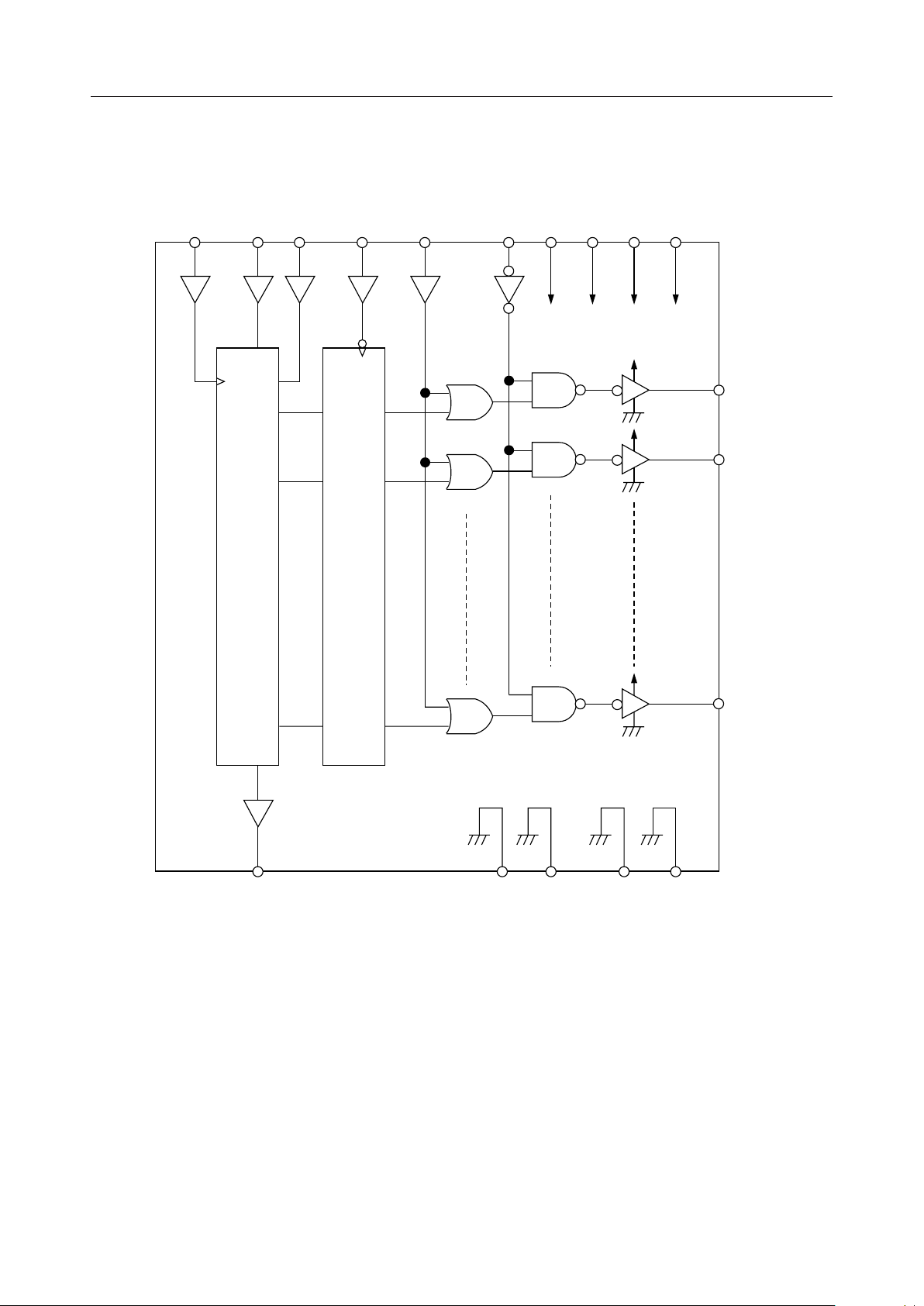
BLOCK DIAGRAM
V
V
V
CLK DIN R/L LS
D
R-1
R-2
11
22
CHG CL
CC
(1 to 20)
CC
(21 to 40)
(1 to 20)
HV
V
HV
(21 to 40)
HVO1
HVO2
40-Bit Latch
40-Bit Bi-directional Shift Register
40 40R-40
Q
DOUT
GND2
(1 to 20)
GND2
(21
to
40)
GND1
(1
to
20)
GND1
(21
to
HVO40
40)
2/13

¡ Semiconductor MSC1163
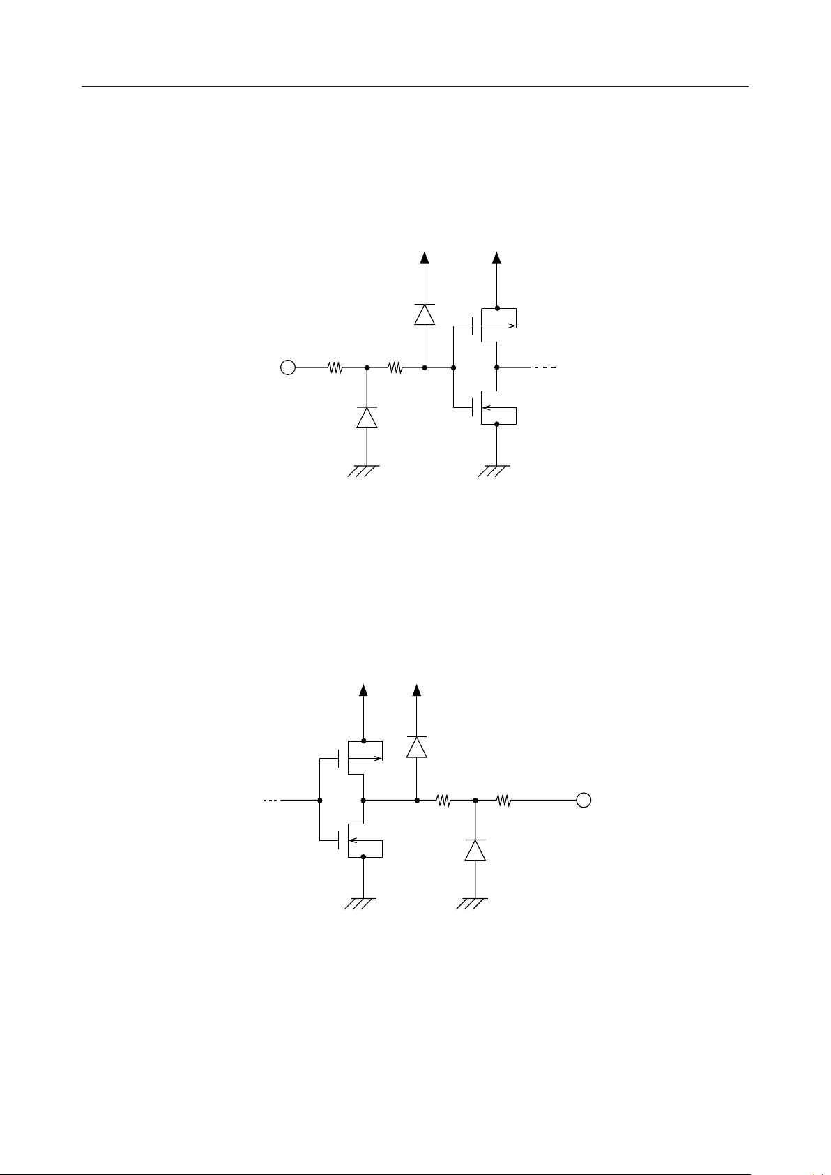
INPUT AND OUTPUT CONFIGURATION
Schematic Diagrams of Logic Portion Input and Output Circuits
Input pin
Output pin
INPUT
V
CC
V
CC
GND1 GND2
V
CC
V
CC
DOUT
GND2 GND1
3/13

¡ Semiconductor MSC1163
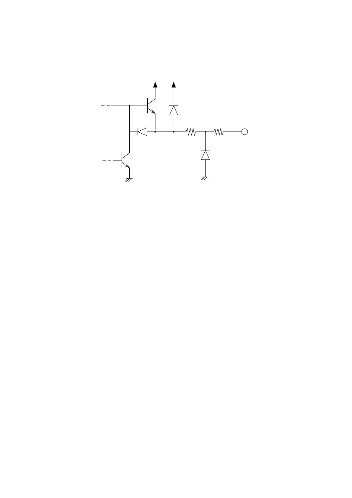
Schematic Diagram of Driver Output Circuit
V
GND 1
HV
V
HV
HVO
GND 1
4/13
 Loading...