

OKI MSC1157MS-K, MSC1157RS Datasheet
E2D0048-39-22
¡ Semiconductor MSC1157
¡ Semiconductor
This version: Feb. 1999
Previous version: May. 1997
MSC1157
Speaker Drive Amplifier
GENERAL DESCRIPTION
The MSC1157, designed specifically to operate at a low voltage with low current consumption,
is a power amplifier developed for driving a speaker for a voice IC.
The voltage gains can be adjusted over a range of up to ten. The differential output can directly
drive a speaker without any output coupling capacitors. The MSC 1157, because of its ability to
stand by, is ideally suitable for portable equipment applications powered by a battery.
FEATURES
• Low voltage operation : 2.0 to 6.0 V (Single power supply)
• Low current dissipation
Operating current : 1.6mA without load (typ.)
• Standby function : Current dissipation less than 1 mA in standby
• High output current : 350mA peak
• Differential outputs : A speaker can be directly connected between
differential outputs.
• Adjustable gain : Gain can be adjusted by use of an external resistor.
• Package options:
8-pin plastic DIP (DIP8-P-300-2.54) (Product name : MSC1157RS)
8-pin plastic SOP (SOP8-P-250-1.27-K) (Product name : MSC1157MS-K)
Chip
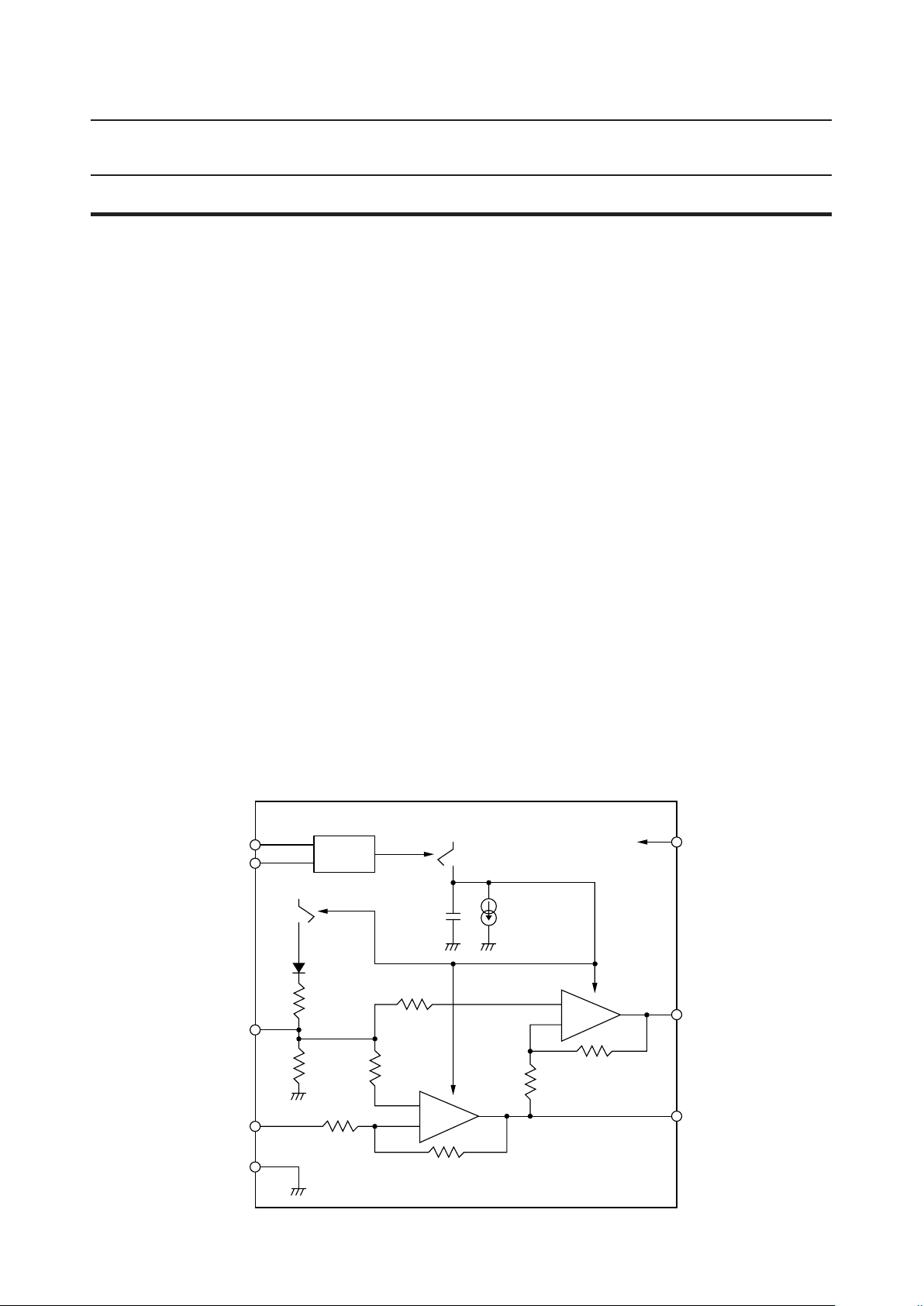
BLOCK DIAGRAM
STBY
SEL
VR
A
IN
GND
V
CC
Logic
V
CC
52 kW50 kW
+
–
20 kW
100 kW
+
–
5 kW
5 kW
V
SP
SP
CC
1/13
¡ Semiconductor MSC1157
PIN CONFIGURATION (TOP VIEW)
PIN DESCRIPTIONS
Pin
5
4
2
Symbol
V
GND — Ground pin.
Type Description
CC
A
IN
— Power supply pin.
I Signal input pin for analog signal inputs, etc.
VR
A
IN
SP
GND
1
2
3
4
8
SEL
7
STBY
6
SP
5
V
CC
8-Pin Plastic DIP
or
8-Pin Plastic SOP
Digital input pins. Setting these pins configures the standby status. See the table below
for how to set the pins.
7, 8
1
STBY,
SEL
VR O
SEL STBY Status
0 Operation
0 1 Standby
Clock Operation
0 Standby
1 1 Operation
I
Clock Operation
0 Operation
Clock 1 Operation
Clock
Unstable Operation
Applying a clock between 32kHz and 4MHz to either the STBY or the SEL pin leads the IC
to operation status regardless of the status set at the other pin. Applying clocks to both
of the pins at the same time may cause malfunction.
Refer to the section, RECOMMENDED OPERATING CONDITIONS since clock frequencies
are changed by setting the SEL pin.
Bias output pin for internal circuits. This pin is at GND potential during standby.
Connecting a capacitor between VR and the GND pin reduces the pop-up noise at power
on and improves the ripple elimination ratio.
3
6
SP O Speaker output pin. This pin outputs a negative phase with respect to the input signal.
SP O Speaker output pin. This pin outputs a positive phase with respect to the input signal.
2/13
¡ Semiconductor MSC1157
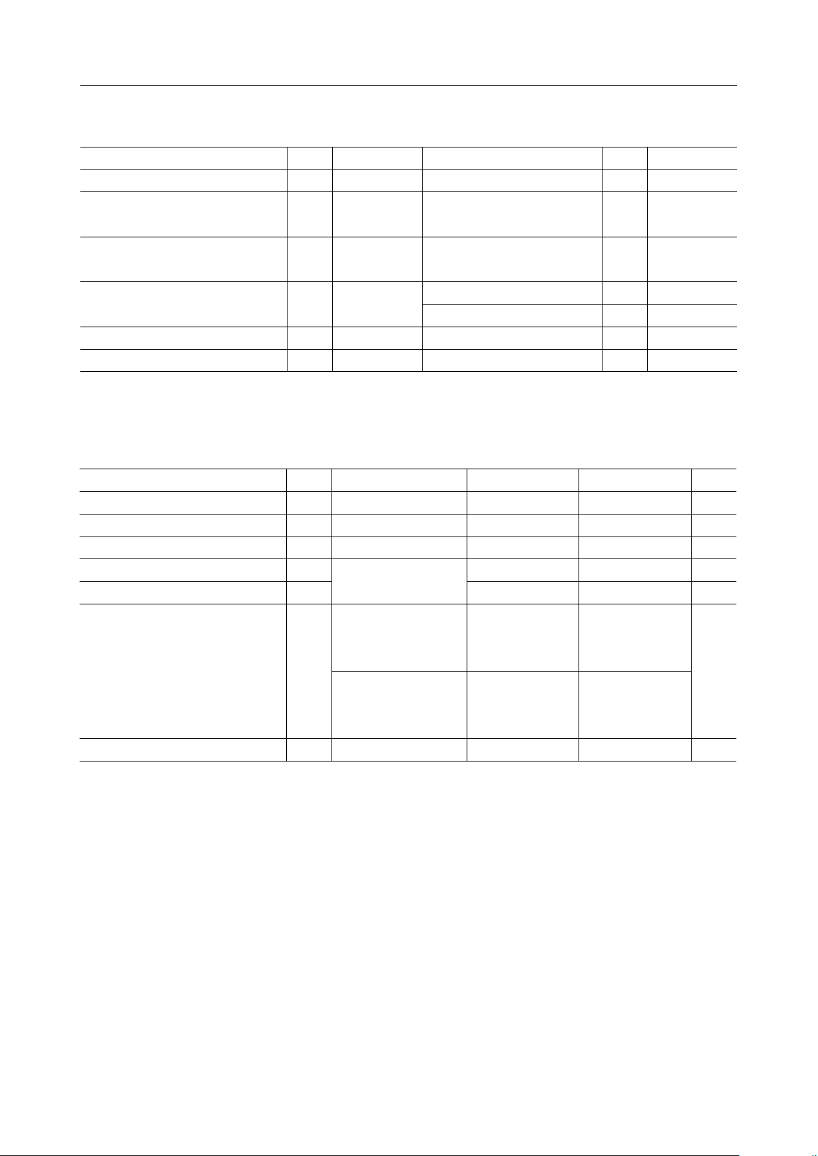
ABSOLUTE MAXIMUM RATINGS
Parameter
Power Supply Voltage V
Symbol
CC
Condition Rating Unit Remark
Ta=25°C –0.3 to +6.5 V V
CC
STBY
Input Voltage V
IN
Ta=25°C –0.3 to VCC+0.3 V
A
IN
, SEL
(*1)
Maximum Output Current I
OMAX
Ta=25°C
±400 mA SP, SP
470 mW DIP type
Power Dissipation P
Junction Temperature
Storage Temperature
T
T
D
jMAX
STG
Ta=25°C
400 mW SOP type
— 125 °C Chip
— –55 to +150 °C
*1 Avoid shorting the output pins (SP and SP) to VCC or GND because the IC may be damaged.
RECOMMENDED OPERATING CONDITIONS
Parameter
Power Supply Voltage V
Load Impedance (*2) RL
Peak Load Current I
"H" Input Voltage V
"L" Input Voltage V
STBY Operating Frequency (*3) f
Operating Temperature Top
Symbol
CC
O-P
IH
IL
STBY
Condition
—
—
—
For STBY and SEL pins
SEL = "L"
At clock input
≥ 2.4 V
V
CC
SEL = "H"
At clock input
≥ 2.4 V
V
CC
—
2.0 6.0 V
8.0 — W
— 350 mA
0.7 V
CC
— 0.3 V
—V
CC
32 k 4.096 M
32 k 1 M
–20 +70 °C
UnitMin. Max.
V
Hz
*2 A speaker of 8 W (standard) or more should be used.
*3 The input of clocks may cause a little noise in output waveforms.
It is recommended to input the DC voltage to inprove voice quality.
3/13
¡ Semiconductor MSC1157
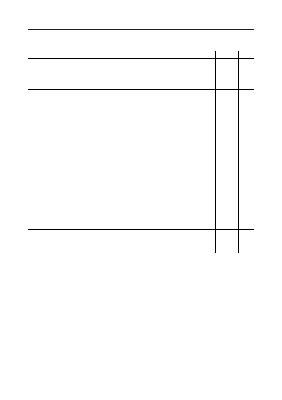
ELECTRICAL CHARACTERISTICS
Unless otherwise specified, Ta=25°C, V
Parameter Symbol Condition UnitMax.Typ.Min.
Input Resistance R
A
IN
Voltage Gain A
IN
A
V1
V2
A
AINÆ(Between SP-SP) 20.512019.46
V3
—kW262014
AINÆSP 14.491413.44
SPÆSP dB+1.580–1.94
VCC=3 V, f=1 kHz
P
OUT1
RL=8 W, THD≥10%
Output Power
VCC=6 V, f=1 kHz
P
OUT2
THD1
Total Harmonic Distortion
THD2
RL=32 W, THD≥10%
V
=3 V, RL=8 W
CC
f=1 kHz, P
=6 V, RL=32 W
V
CC
f=1 kHz, P
=45 mW
OUT
=125 mW
OUT
Ripple Elimination Ratio RR f=1 kHz, C2=4.7 mFdB—4330
Output DC Voltage
(*4)
V
Output Offset Voltage DV
O
signal state
O
In no
Between SP-SP mV±30——
VCC=2 V 0.770.650.53
=6 V 2.732.612.49
V
CC
AIN=VCC or GND
V
OH
I
=–100 mA
OUT
AIN=VCC or GND
Output "L" Voltage
STBY, SEL
Input Current
VR Equivalent Resistance R
Circuit Current During Operation I
Circuit Current During Standby I
V
I
I
CCS
OL
IH
IL
VR
CC
=100 mA
I
OUT
VI=V
CC
VI=GND mA±0.1——
—
VCC=6 V, RL=• mA2.41.61.1
— mA1.0——
CC
=2 to 6 V
CC
mW—178100
mW—440300
%—1.2—
%—0.37—
V
–1.04VCC–1.15Output "H" Voltage
V—V
V0.30.17—
mA±0.1——
kW322518
*4 The typical value of the output voltage in no signal state is determined from the following
equation.
50 kW
VO = (V
CC
– 0.67)
50 kW + 52 kW
4/13

¡ Semiconductor MSC1157
APPLICATION CIRCUIT
+
C4 C3
–
Standby
Select
Input
Standby
Input
Audio
Input
C1
SEL
STBY
A
IN
VR
+
C2
–
V
CC
GND
SP
Speaker
SP
• If parasitic capacitance of 60pF or more exists between GND and the speaker output pin SP or
SP, oscillation may occur. Implement the circuit mount design so as to be less than 60pF.
• C1 is the AC coupling capacitor. Cutoff frequency fc on the low frequency side is determined
by the following equation. Choose a value of C1 according to the bandwidth.
1
fc =
(Hz)
2 ¥ p ¥ C1 ¥ 20k
• Choose a value of C2 that is 80 to 100 times as large as that of C1.
• When the standby function is not used, connect the pins STBY and SEL to VCC or GND.
• It is recommended that the capacitor C4 (approximately 0.1mF) having better high frequency
characteristics and the capacitor C3 (approximately 10mF) be placed between the pins VCC and
GND.
5/13
 Loading...